Introduction
From an Information and Communications Technology (ICT) perspective, the 21st century is characterized by an explosion of requests for computing, storage, and communications capabilities. Over the past few years, global Internet traffic has been growing exponentially. In this picture, the “bottleneck” is represented by the difficulties in moving digital information on different scales, ranging from worldwide links to chip-to-chip and intrachip interconnections. Optical interconnects combined with integrated circuits is seen as one of the most promising routes to solve this problem.Reference Miller1 There have also been suggestions to translate this approach to the mid-infrared (MIR) wavelength range,Reference Soref, Emelett and Buchwald2–Reference Jalali, Raghunathan, Shori, Fathpour, Dimitropoulos and Stafsudd4 a transparent window of the atmosphere that encompasses absorbing lines of many gaseous or organic species, thus, the best window for developing integrated and compact spectroscopy instruments.
The availability of integrated light sources is therefore a key technology for the whole silicon photonics industry. Silicon-based sources could directly bridge the gap, but the indirect bandgap of Si and Ge is a severe limitation,Reference Jalali and Fathpour5 and, in spite of recent advances,Reference Rong, Jones, Liu, Cohen, Hak, Fang and Paniccia6–Reference Wirths, Geiger, von den Driesch, Mussler, Stoica, Mantl, Ikonic, Luysberg, Chiussi, Hartmann, Sigg, Faist, Buca and Grützmacher8 these devices will not, in the foreseeable future, outperform their III–V semiconductor counterparts that currently represent the most efficient semiconductor laser technology. Much effort has been directed toward hybrid integration of III–V lasers with Si-photonics platforms where III–V wafers or dies are bonded onto silicon photonics circuits. Although impressive results have been achieved,Reference Tanabe, Watanabe and Arakawa9,Reference Duan, Olivier, Malhouitre, Accard, Kaspar, de Valicourt, Levaufre, Girard, Le Liepvre, Shen, Make, Lelarge, Jany, Ribaud, Mallecot, Charbonnier, Gariah, Kopp and Gentner10 on a longer term, large-scale integration of photonic circuits will rely on monolithic integration of laser sources on silicon.
The idea of integrating III–V materials (monolithically grown) on silicon is, of course, not new. First investigations started in the 1980s and continued in the 1990s with InP on silicon, especially at Nippon Telephone and Telegraph Laboratories in Japan.Reference Sugo, Mori, Itoh, Sakai and Tachikawa11,Reference Yamada, Tachikawa, Sasaki, Mori and Kadota12 However, monolithic III–V/Si integration faces significant challenges as a result of the large material dissimilarity between III–V and Group IV materials, including lattice mismatch, thermal expansion coefficient differences, and polar versus nonpolar surfaces. These differences between III–V and Group IV materials tend to produce various types of defects—antiphase boundaries (APBs), threading dislocations (TDs), and microcracks—which all generate nonradiative recombination centers and dramatically undermine the promise of III–V materials.Reference Zimmermann13 Still, the past decade has seen new momentum for III–V on Si epitaxy driven by the latest knowledge accumulated in the field of heteroepitaxy and by the importance of integrating III–V optoelectronic devices and silicon photonics platforms.
In this article, we review recent progress made in the direct growth of metamorphic III–V lasers on silicon substrates. We first briefly address issues related to the silicon substrate itself before moving to results on lasers formed using III–V semiconductor materials systems (GaSb, GaAs, and GaP).
Si substrate orientation and preparation
The long-term vision for silicon photonics calls for the integration of III–V devices on so-called “exact” (001) Si substrates (i.e., substrates with a miscut less than 0.5°). However, APBs can emerge when growing III–V materials on silicon due to the polar/nonpolar nature of the III–V/Si interface. In order to achieve APB-free III–V layers, either a perfect doubling of the height of all silicon surface stepsReference Kroemer14 or self-annihilation of all APBs must be achieved.
Factors influencing step formation on silicon have already been thoroughly studied. In brief, single-layer steps generally form on exact (001) Si surfaces, while double-layer steps become increasingly stable when increasing the miscut angle of (001) substrates misoriented toward 〈011〉.Reference Kroemer14 Consequently, the growth of III–V semiconductors on Si substrates is mainly performed using miscut (001) Si substrates in order to promote double-step formation and to minimize the number of APBs in the growing III–V semiconductor. This is the case for the lasers presented in the following sections that are grown on substrates exhibiting a 4–6° miscut angle.
Whatever the orientation, the quality of the silicon surface prior to epitaxy is key for the control and reproducibility of III–V epitaxy on silicon. The silicon surface needs to be perfectly plane and clean before III–V epitaxy. Indeed, the presence of contaminants such as oxides or carbon, metal, or organic impurities on the surface may lead to the formation of defects during growth.Reference Ishizaka and Shiraki15,Reference Kern16 Such defects are detrimental to device performance and are an efficient and reliable substrate surface preparation before epitaxy is mandatory. Most III–V epitaxial reactors do not allow heating of the substrate to over 1000°C, which is needed to perform in situ surface cleaning and preparation. Different ex situ preparation techniques have thus been proposed over the years, and it has now become clear that efficient approaches rely on cycles combining oxide removal/hydrogen passivation/controlled oxidation sequences.Reference Madiomanana, Bahri, Rodriguez, Largeau, Cerutti, Mauguin, Castellano, Patriarche and Tournié17 Such sequences are now employed by most research groups, albeit using different processes.
GaSb-based quantum-well lasers
Among III–V compounds, the so-called “antimonides” or III–Sbs are based on GaSb, InAs, InSb, AlSb, and their alloys. Particularly relevant to silicon photonics, III–Sb laser diodes grown on GaSb substrates have demonstrated high-performance continuous-wave (CW) operation at room temperature (RT) between wavelengths of 1.55 µm and 3.4 µm,Reference Tournié, Baranov, Coleman, Brice and Jagadish18,Reference Cerutti, Castellano, Rodriguez, Bahri, Largeau, Balocchi, Madiomanana, Lelarge, Patriarche, Marie and Tournié19 while III–Sb interband cascade lasersReference Vurgaftman, Weih, Kamp, Meyer, Canedy, Kim, Kim, Bewley, Merritt, Abell and Höfling20 and quantum-cascade lasers bridge the gap up to 20 µm.Reference Bahriz, Lollia, Baranov and Teissier21 GaSb technology thus covers the whole spectral range from ICT to sensing.
III–Sb on Si epitaxial growth
The preferred growth technique for GaSb-based compounds and heterostructures is solid-source molecular beam epitaxy (MBE), the only technique yielding device-grade material.Reference Tournié, Baranov, Coleman, Brice and Jagadish18 Other peculiarities of this material system are (1) the use of mixed Group V quaternary or quinary alloys and (2) the presence of no common-atom interfaces. This requires implementing dedicated growth strategies that are beyond the scope of this article. However, the use of Sb valved-cracker cells that generate Sb2 molecules and allow precise flux control is essential to grow reproducible, high-quality material. All results discussed hereafter have been obtained by MBE.
The lattice mismatch between GaSb and Si is as high as ∼13%. Therefore, strain relaxation should start at a thickness below one monolayer. Interesting observations have been made with III–Sb semiconductors grown on silicon. Huang et al. showed that strain relaxation can occur by the formation of pure edge-type misfit dislocations (MDs), instead of a high density of TDs, arranged in a two-dimensional (2D) network confined at the III–Sb/Si interface.Reference Huang, Balakrishnan, Khoshakhlagh, Dawson and Huffaker22,Reference Kim, Noh, Kim, Oh and Chung23 A beneficial aspect of III–Sb-based materials is their relative softness that lowers the energy barrier for the nucleation of MDs as compared to stiffer materials such as arsenide, phosphide, or nitride semiconductors. These sessile MDs, in turn, are the most efficient defects to relieve the strain in highly mismatched materials systems, and they cannot easily propagate out of the (001) interface plane into the subsequently grown layers.Reference Trampert, Tournié and Ploog24 In principle, this particular relaxation mode should lead not only to a highly defective interface, but also to improved crystal quality of the III–Sb layer grown atop without resorting to several-µm-thick buffer layers. This is an important difference compared to other III–V-on-Si materials systems where thick and complex buffer layers are generally used (as detailed in the section on GaAs).
Finally, a key point in the MBE growth of III–Sbs on silicon is the insertion of an AlSb nucleation layer (NL) prior to any GaSb growth. Although the mechanisms at work are not yet clear, this layer dramatically improves the crystal quality of the epitaxial material.Reference Akahane, Yamamoto, Gozu and Ohtani25 More work is needed to elucidate mechanisms at work on a microscopic scale.
MIR GaSb-based lasers grown on Si
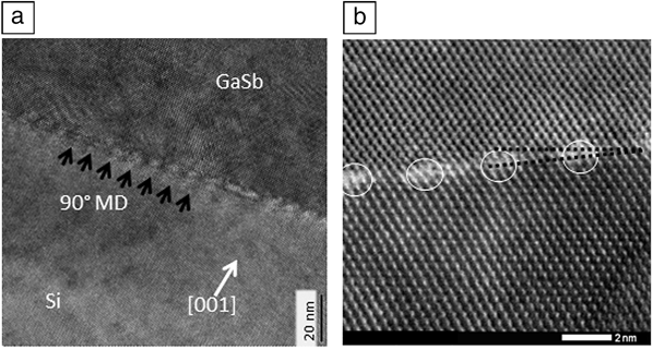
Although early demonstrations of light-emitting devices in the 1.5–2.1 µm wavelength range were reported at 77 K,Reference Jallipalli, Kutty, Balakrishnan, Tatebayashi, Nuntawong, Huang, Dawson, Huffaker, Mi and Bhattacharya26,Reference Tatebayashi, Jallipalli, Kutty, Huang, Nunna, Balakrishnan, Dawson and Huffaker27 much more work was needed before RT lasing could be demonstrated. The first demonstration of RT lasing relied on a typical GaSb-based laser structure grown on a 1-µm-thick GaSb buffer layer.Reference Rodriguez, Cerutti, Grech and Tournié28Figure 1 shows transmission electron microscope (TEM) images of the interface where one can clearly see the presence of a network of MDs and the miscut angle, in agreement with previous observations.Reference Huang, Balakrishnan, Khoshakhlagh, Dawson and Huffaker22,Reference Kim, Noh, Kim, Oh and Chung23 Such TEM images are representative of all GaSb-on-Si samples.
Cross-sectional transmission electron microscope images of a GaSb/Si interface revealing the presence of a network of 90° misfit dislocations (MDs), black arrows in (a), white circles in (b) at the interface and the miscut angle, dotted gray lines in (b). Courtesy of A. Trampert, PDI-Berlin.

Figure 2 shows the light–current (L–I) characteristics obtained in CW at various temperatures for a laser diode in an electrical configuration with both the n- and p-contacts on top of the device.Reference Reboul, Cerutti, Rodriguez, Grech and Tournié29 The threshold current density is as low as ∼900 A·cm–2 and the lasing wavelength is near 2 µm at RT. CW laser operation is achieved up to 35°C, the highest temperature allowed by the experimental setup. The CW output power measured under a maximum drive current of 350 mA varies between 8 mW/facet and 2 mW/facet when the temperature is ramped from 10°C to 35°C. The external quantum efficiency ƞd, obtained from the slope of the L–I curves, changes from 16% to 12% in this temperature range. These values are only slightly lower than those obtained with state-of-the-art laser diodes grown on GaSb and show the potential of this approach to be extended to the whole 2–3 µm wavelength range where GaSb-based laser diodes perform best.Reference Tournié, Baranov, Coleman, Brice and Jagadish18
Continuous-wave (CW) output power–current–voltage characteristics of “top–top” GaSb-based laser diodes grown on Si. Right axis: output power versus injected current for different temperatures. Left axis: voltage–current curve at 20°C. The inset shows the lasing spectrum taken at 20°C under 300-mA CW injection. High-performance lasing is achieved in this configuration. Reprinted with permission from Reference Reference Reboul, Cerutti, Rodriguez, Grech and Tournié29. © 2011 American Institute of Physics.
Telecom GaSb-based lasers grown on Si
Less effort has been devoted to developing GaSb-based devices in the 1.5-µm telecom wavelength range. Indeed, band-structure engineering is critical to get from the 2-µm wavelength range down to around 1.55 µm. The key point is ensuring high enough carrier confinement in the conduction and valence-band QWs engineered through a strain above 1%.Reference Cerutti, Rodriguez and Tournié30 These lasers performed well when grown on GaSb substrates, with threshold current densities around 350 A·cm–2. Their performance on Si substrates, however, was limited with threshold current densities around 1 and 5 kA cm–2 at 90 K and RT, respectively.Reference Cerutti, Rodriguez and Tournié30 More efficient QWs have been recently designed and developedReference Cerutti, Castellano, Rodriguez, Bahri, Largeau, Balocchi, Madiomanana, Lelarge, Patriarche, Marie and Tournié19 that could readily be applied to metamorphic lasers on silicon to develop a Si-photonics telecom source.
Perspectives
Much progress has been made in the past few years on GaSb-based lasers grown on Si via simple (a GaSb layer) and thin (1 µm) buffer layers. This is a peculiarity of this technology, since other approaches resort to complex and thick buffer layers, as discussed in the next section. Still, there is room for improvement to attain threshold current densities closer to those achieved on GaSb substrates, particularly through elucidating the mechanisms of strain relaxation and defect formation at the III–Sb/Si interface. Indeed, even though MD formation has now been demonstrated, interactions of MDs being out of registry due to surface irregularities (e.g., three-dimensional nucleation and coalescence, surface steps, impurities) results in the generation of threading dislocations.Reference Djafari Rouhani, Kassem, Dalla Torre, Landa, Rocher and Estève31 Such detailed studies will open the route to low-threshold GaSb-based lasers emitting in the whole 1.5–3 µm wavelength range.
GaAs-based quantum dot lasers grown on Si
Impressive results have been achieved in the last decade for InGaAs quantum dot (QD) lasers on Si with lasers operating at 1.05 µm.Reference Mi, Bhattacharya and Yang32 Bhattacharya’sReference Mi, Yang, Bhattacharya, Qin and Ma33 and Liu’sReference Lee, Liu and Seeds34,Reference Wu, Chen, Seeds and Liu35 groups have previously published review papers in this area. In this section, recent progress on realizing high-performance 1.3-μm InAs/GaAs QD lasers grown on silicon is reviewed.
QD lasers monolithically grown on silicon
To date, the fundamental obstacle limiting monolithic growth of III–V lasers on silicon has been the formation of high-density TDs introduced by large lattice mismatch and thermal expansion coefficient mismatch between III–V materials and silicon substrates. To overcome this roadblock, the growth of a GaAs NL was first explored to reduce the density of TDs by effectively confining defects at the interface between the GaAs metamorphic buffer and silicon substrate.Reference Wang, Liu, Lee, Pozzi and Seeds36
As shown in Figure 3a–c, TEM results revealed that controlling the growth temperature of the initial GaAs NL has become crucially important, typically with the lowest TDs and best photoluminescence (PL) intensity achieved at 400°C (shown in Figure 3d).Reference Wang, Liu, Lee, Pozzi and Seeds36,Reference Lee, Jiang, Tang, Zhang, Seeds and Liu37 Based on this template, a five-layer InAs/GaAs dot-in-well laser structure was grown on silicon substrates. An electrically pumped InAs/GaAs QD laser epitaxially grown on a Si substrate was demonstrated for the first time at 1.3 µm with a threshold current density of 725 A/cm2 and output power of 26 mW at RT, as shown in Figure 3e. Lasing operation up to 42°C was obtained (see Figure 3f). To further optimize the III–V NL on Si substrates, a new type of AlAs NL was developed to further reduce the TDs within the GaAs metamorphic buffer layer on silicon substrates.Reference Lee, Jiang, Tang, Zhang, Seeds and Liu37 AlAs NL was found to be more effective in terms of confining defects within the AlAs/Si interface region and, consequently, fewer defects propagated into the GaAs buffer. The Si-based InAs/GaAs QD laser with an AlAs NL was demonstrated with a threshold current density of 650 A/cm2 at RT and lasing up to 63°C.Reference Lee, Jiang, Tang, Zhang, Seeds and Liu37
Cross-sectional transmission electron microscope images of GaAs/Si interface with the initial GaAs nucleation layer (NL) grown at (a) 380°C, (b) 400°C, and (c) 420°C. (d) Room-temperature (RT) photoluminescence (PL) spectra of InAs/GaAs quantum dots (QDs) grown on Si substrates with different temperatures for the initial GaAs NL and RT PL spectrum of InAs/GaAs QDs reference sample grown on a GaAs substrate. The inset shows a 1 µm ×1 µm atomic force microscope image of uncapped InAs/GaAs QDs grown on a Si substrate with the initial GaAs NL grown at 400°C. (e) Output power–current density (L–J) characteristics of a 3000 µm × 50 µm InAs/GaAs QDs laser grown on a Si substrate under pulsed conditions at RT. The inset shows the lasing spectrum just above the threshold. (f) L–J characteristics of a 3000 µm × 50 µm InAs/GaAs QDs laser grown on a Si substrate at various heatsink temperatures under pulsed operation. The first electrically pumped 1.3 μm InAs/GaAs QD laser grown directly on a Si substrate is achieved in this configuration. Reprinted with permission from Reference Reference Wang, Liu, Lee, Pozzi and Seeds36. © 2001 The Optical Society. Note: J, current density.
Apart from the III–V NL, the use of a dislocation filter layer (DFL) is another important method to reduce the defect density in III–V metamorphic buffer layers. In general, strained-layer superlattices (SLSs) can effectively suppress the propagation of TDs by bending the TDs into the growth plane and hence, acting as DFLs.Reference Tang, Chen, Wu, Jiang, Dorogan, Benamara, Mazur, Salamo, Seeds and Liu38,Reference Chen, Tang, Wu, Jiang, Dorogan, Benamara, Mazur, Salamo, Seeds and Liu39 Both InGaAs/GaAs and InAlAs/GaAs SLSs have been explored as DFLs in GaAs metamorphic buffer layers on silicon substrates. Cross-sectional TEM, etch-pit density, and PL measurements were employed to compare the TDs and optical properties of samples using InAl(Ga)As/GaAs SLSs, as shown in Figure 4a–d, where InAlAs/GaAs SLSs were found to be more effective in blocking propagation of TDs than InGaAs/GaAs SLSs.Reference Tang, Chen, Wu, Jiang, Dorogan, Benamara, Mazur, Salamo, Seeds and Liu38
Dark-field multibeam cross-sectional transmission electron microscope (TEM) images of GaAs buffer grown on Si substrates with (a) InGaAs/GaAs dislocation filter layers (DFLs) and (b) InAlAs/GaAs DFLs. The scale bars in (a) and (b) are 1 μm. (c) Reduction of threading dislocations induced by DFLs measured by TEM and etch-pit density (EPD) measurements at different positions. (d) Room-temperature (RT) photoluminescence (PL) spectra of InAs/GaAs quantum dots (QDs) grown on a Si substrate with InGaAs and InAlAs DFLs, respectively. (e) Single-facet output power versus current density of a 3000 µm × 25 µm InAs/GaAs QDs laser grown on a Si substrate with InAlAs/GaAs DFLs under pulsed operation at RT. The inset shows the emission spectra below (purple) and just above (red) the threshold. (f) Light output power versus current density for an InAs/GaAs QD laser grown on a Si substrate at various heatsink temperatures. The inset shows the lasing spectrum of a 3000 µm × 25 µm InAs/GaAs QD laser grown on Si at 111°C under pulsed operation. High-performance Si-based lasers with low threshold current density, high output power, and high lasing operation temperature are achieved in this configuration. Reprinted with permission from Reference Reference Tang, Chen, Wu, Jiang, Dorogan, Benamara, Mazur, Salamo, Seeds and Liu38. © 2014 The Optical Society. Reprinted with permission from Reference Reference Chen, Tang, Wu, Jiang, Dorogan, Benamara, Mazur, Salamo, Seeds and Liu39. © 2014 IEEE Publishing. Note: J, current density; T, temperature; EPD, etch pit density.
A standard five-layer InAs/GaAs QD laser structure was then developed by utilizing the combined effect of InAlAs/GaAs SLSs serving as DFLs and an AlAs NL. The Si-based laser device performance is presented in Figure 4e–f. This Si-based laser achieves lasing operation up to 111°C with a low threshold current density of 200 A/cm2 and output power/facet of >100 mW at RT.Reference Chen, Tang, Wu, Jiang, Dorogan, Benamara, Mazur, Salamo, Seeds and Liu39 This combination of AlAs NL and InAlAs/GaAs DFLs was also employed to develop the 1.3-μm InAs/GaAs QDs superluminescent light-emitting diodes grown on silicon substrates.Reference Chen, Tang, Jiang, Wu, Dorogan, Benamara, Mazur, Salamo, Smowton, Seeds and Liu40,Reference Chen, Tang, Wu, Jiang, Dorogan, Benamara, Mazur, Salamo and Liu41 It should be noted that GaAs-based 1300-nm QD lasers grown on Ge and Ge-on-Si substrates have also been developed as an alternative approach for silicon photonics in the last few years.Reference Liu, Wang, Jiang, Hogg, Tutu, Pozzi and Seeds42–Reference Liu, Srinivasan, Norman, Gossard and Bowers45 Thanks to the small lattice mismatch and comparable thermal expansion coefficient, QD lasers on Ge and Ge-on-Si substrates have shown superior performance than that directly on Si substrates.
GaP-based lasers and virtual substrates grown on Si
Recently, the concept of monolithic growth of direct bandgap Ga(NAs)P based on GaP substrates on (001) silicon substrates is being studied. Since GaP is quasi-lattice matched to Si substrates, the formation of TDs can be minimized, and APB-free layers have been demonstrated by metal–organic vapor-phase epitaxy.Reference Voltz, Beyer, Witte, Ohlmann, Németh, Kunert and Stolz46 A GaP/Si virtual substrate can then be fabricated that allows decoupling the problems related to the nonpolar/polar interface and to strain relaxation. Interesting studies on GaP-based devices grown on silicon substrates have been presented.Reference Thanh, Robert, Guo, Letoublon, Cornet, Elias, Ponchet, Rohel, Bertru, Balocchi, Durand, Micha, Perrin, Loualiche, Marie and Le Corre47 Lasing operations between 800 and 900 nm have been achieved under optical pumping and pulsed operation conditions, but remain limited to 150 K.Reference Liebich, Zimprich, Beyer, Lange, Franzbach, Chatterjee, Hossain, Sweeney, Volz, Kunert and Stolz48 New material heterostructures will probably have to be used in order to achieve more favorable band structures.Reference Gauthier, Robert, Almosni, Leger, Perrin, Even, Balocchi, Carrère, Marie, Cornet and Durand49,Reference Song and Lee50 In another approach, a GaP/Si template was used as a virtual substrate to InGaAs/GaAs QW laser diodes. RT lasing under pulsed operation was demonstrated near 1.03 µm, which is promising for future developments.Reference Huang, Song, Masuda, Jung and Lee51
Conclusion
In this article, we have reviewed current progress in III–V lasers monolithically integrated on silicon substrates. Recent advances in the control of metamorphic growth have allowed the demonstration of RT, CW laser emission over the 1.0–2.0 µm wavelength range, which can be further extended at both ends. Current studies under way in various laboratories are expected to result in still better understanding and mastering of strain relaxation and defect formation, thus further enhancing performance. These achievements and prospects confirm that the metamorphic growth of III–V compounds is a technique of choice for integrating optolectronic devices with silicon platforms and open great potential for future applications of silicon photonics.
Acknowledgments
Part of the authors’ work has been supported by the French “Investment for the Future” program (EquipEx EXTRA, ANR-11-EQPX-0016), by the French ANR (OPTOSi, ANR-12-BS03–002), and by UK EPSRC under Grant No. EP/J012904/1. E.T. gratefully acknowledges support from the Institut Universitaire de France (IUF) and A. Trampert (PDI, Berlin) for TEM analysis.