Introduction
Manipulating thermal-transport properties is important for various applications ranging from integrated circuits and optoelectronics to thermoelectric energy conversion.Reference Moore and Shi1,Reference Tian, Lee and Chen2 Thermoelectric generators, capable of realizing direct energy conversion from heat into electricity, are solid-state devices with broad future promise for low-grade waste heat harvesting. The conversion efficiency is dominated by the material’s dimensionless thermoelectric figure of merit:
 $$ZT = \left( {{{{S^2}\sigma } / \kappa }} \right)T,$$
where S, σ, κ, and T are the Seebeck coefficient, electrical conductivity, total thermal conductivity (including contributions from lattice, κlat , and electrons, κel), and absolute temperature, respectively. For more than a half century, a ZT of approximately 1 has been generally considered as the benchmark for pursuing high ZT.
Stimulated by the concept of “quantum confinement” coupled with the introduction of advanced synthesis techniques,Reference Hicks and Dresselhaus3,Reference Hicks and Dresselhaus4 a series of record-high ZT values have been realized for materials and structures ranging from quantum dots (zero-dimensional structures) to bulk nanostructured materials (three-dimensional [3D] structures) over the past two decades.Reference Dresselhaus, Chen, Tang, Yang, Lee, Wang, Ren, Fleurial and Gogna5–Reference Tan, Zhao and Kanatzidis7 These critical advances are mainly attributed to reduced κlat, since κlat is relatively independent of the electronic properties.Reference Zhu, Liu, Fu, Heremans, Snyder and Zhao8 Generally, heat conduction in a semiconductor is mostly dominated by lattice vibrations, which can be approximately understood using kinetic theory:
 $${\kappa _{{\rm{lat}}}} = {1 \over 3}{C_{\rm{v}}}vl,$$
where C v is the specific heat of the semiconductor, ν is the phonon group velocity, and l is the phonon mean free path (MFP). Heat transport in thermoelectric materials results from the cumulative contributions of phonons with a broad range of MFPs, and different MFPs contribute different amounts to κlat for a specific material.Reference Minnich, Johnson, Schmidt, Esfarjani, Dresselhaus, Nelson and Chen9 Taking bulk crystalline silicon as a representative example, its MFP spectrum spans more than five orders of magnitude from 1 nm to 100 μm at room temperature.Reference Esfarjani, Chen and Stokes10 Thus, designing multiscale microstructures encompassing point defects, linear defects, interfacial defects, and volume defects could scatter phonons across a wide range of length scales, maximally suppress κlat, and thereby increase ZT.Reference Poudel, Hao, Ma, Lan, Minnich, Yu, Yan, Wang, Muto, Vashaee, Chen, Liu, Dresselhaus, Chen and Ren11–Reference Kim, Lee, Mun, Kim, Hwang, Roh, Yang, Shin, Li, Lee, Snyder and Kim14
For practical applications of thermoelectric materials, bulk nanostructured materials hold great promise for commercialization due to their practicability, compared to quantum dots, nanowires, and superlattices.Reference Minnich, Dresselhaus, Ren and Chen15 By designing special nano-microstructures to tailor thermal conductivity, we have witnessed great progress in bulk high-performance materials for thermoelectric applications, especially boosting large-scale energy-harvesting applications. In this article, we provide an overview of the reasons for the formation of as well as phonon-scattering mechanisms of microstructural defects, highlight the role of hierarchical microstructures and point out challenges in related simulations.
Phonon engineering via microstructural defects
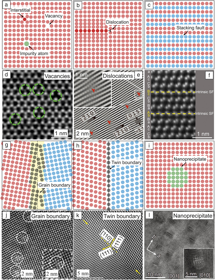
Real materials are not perfect, and defects will inevitably scatter phonons. Phonon MFP or relaxation time, τ, depends upon phonon scattering by microstructural defects in addition to intrinsic phonon–phonon scattering. Manipulating phonon transport by designing defects is feasible. Figure 1 shows schematic diagrams and corresponding high-resolution transmission electron microscope images of common defects in solids.Reference Biswas, He, Blum, Wu, Hogan, Seidman, Dravid and Kanatzidis12,Reference Kim, Lee, Mun, Kim, Hwang, Roh, Yang, Shin, Li, Lee, Snyder and Kim14,Reference Hong, Hu, Probert, Li, Lv, Yang, Gu, Mao, Feng, Xie, Zhang, Wu, Zhang, Jin, Ji, Zhang, Yuan and Zhang16–Reference Mao, Wang, Liu, Ge and Ren18
Schematic diagrams and corresponding high-resolution transmission electron microscope images of common defects in solids. (a, d) Vacancies. Reprinted with permission from Reference Reference Hong, Hu, Probert, Li, Lv, Yang, Gu, Mao, Feng, Xie, Zhang, Wu, Zhang, Jin, Ji, Zhang, Yuan and Zhang16. © 2015 Nature Publishing Group. (b, e) Dislocations. Reprinted with permission from Reference Reference Kim, Lee, Mun, Kim, Hwang, Roh, Yang, Shin, Li, Lee, Snyder and Kim14. © 2015 AAAS. (c, f) Stacking faults (SFs).Reference Mao, Wang, Liu, Ge and Ren18 (g, j) Grain boundaries. Reprinted with permission from Reference Reference Wu, Pei, Wang, Wu, Huang, Zhao and He17. © 2014 Wiley. (h, k) Twin boundaries.Reference Mao, Wang, Liu, Ge and Ren18 (i, l) Nanoprecipitates. Reprinted with permission from Reference Reference Biswas, He, Blum, Wu, Hogan, Seidman, Dravid and Kanatzidis12. © 2012 Nature Publishing Group. The insets in (e), (j), and (l) show the morphology of a dislocation, dislocation (on the grain boundary), and nanoprecipitate, respectively.
Point defects are usually thermodynamically stable due to the balance between increased crystal distortion energy and system entropy;Reference DeHoff19 these include vacancies, interstitials, and impurity atoms. Vacancies are the primary intrinsic point defects owing to their low formation energy.Reference DeHoff19 Tuning the stoichiometric composition or extrinsic methods (e.g., radiation treatment) can control the vacancy concentration in semiconductors.Reference Liu, Zhao, Liu, Lan, Xu, Li, Zhang, Berardan, Dragoe and Lin20,Reference Tuomisto, Ranki, Saarinen and Look21 Interstitials are high-energy defects that are less common than other point defects.Reference DeHoff19 In some cases, small atoms tend to occupy octahedral or tetrahedral interstitial sites of a cubic lattice or van der Waals gaps of lamellar structures.Reference Hu, Zhu, Liu and Zhao22 In thermoelectric materials, impurity atoms are more common due to the requirement of decreasing the thermal conductivity or optimizing the carrier concentration. Antisite defects may also occur in an ordered alloy or compound (e.g., Bi locating to Te sites in Bi2Te3).Reference Zhu, Hu, Zhao and He23
Phonon scattering by point defects mainly arises from mass and strain fluctuations.Reference Callaway and von Baeyer24 Vacancies and interstitials, which are considered the strongest phonon-scattering centers, can maximize these fluctuations. Rattling fillers in skutterudites, which have the general formula RM4X12 (R is normally rare-earth elements, M is Fe, Ru, or Os, and X is P, As, or Sb), could effectively reduce κlat due to resonant scattering and other factors, for example, the reduced group velocity of phonons.Reference Yang, Xi, Qiu, Wu, Shi, Chen, Yang, Zhang, Uher and Singh25 However, the concentration of defects plays a critical role in the phonon–impurity coupling strength, and therefore, isoelectronic substitution could dramatically suppress κlat, especially for heavy elements.Reference He, Zhu, Sun, Mao, Reith, Chen, Schierning, Nielsch and Ren26
Linear defects or dislocations were first introduced to explain the low fracture strength of real materials.Reference Hull and Bacon27 Plastic deformation is the most commonly used method to increase the dislocation density in metal.Reference Kuhlmann-Wilsdorf28 Due to the low density of dislocations at equilibrium in semiconductors, phonon scattering by dislocations has long been overlooked in thermoelectrics. Recently, liquid-phase compaction was used to produce low-angle grain boundaries with dense dislocation arrays, as demonstrated in Bi0.5Sb1.5Te3 and Yb-filled CoSb3.Reference Kim, Lee, Mun, Kim, Hwang, Roh, Yang, Shin, Li, Lee, Snyder and Kim14,Reference Meng, Liu, Cui, Qin, Geng, Cai, Fu, He, Ren and Sui29 Dislocation loops can be generated by the collapse of vacancy discs in lead chalcogenides,Reference Chen, Ge, Li, Lin, Shen, Chang, Hanus, Snyder and Pei30,Reference Chen, Jian, Li, Chang, Ge, Hanus, Yang, Chen, Huang, Snyder and Pei31 which was initially observed in metals.Reference Hirsch, Silcox, Smallman and Westmacott32
A dislocation consists of a core and an elastic stress field, hence in principle, phonon scattering via dislocations can have two distinctive mechanisms.Reference Carruthers33 Scattering via dislocation cores can be considered a short-range-interaction model similar to mass-difference impurity scattering, whereas phonon scattering via the elastic field shows long-range characteristics that depend on the type of dislocation.Reference Carruthers33 Recently, the concept of a “dislon,” a quantized quasiparticle of dislocation that can interact with elastic waves, has been used to explore the nonperturbative nature of coupling between a dislocation and a phonon.Reference Li, Ding, Meng, Zhou, Zhu, Liu, Dresselhaus and Chen34
Interfacial defects mainly include grain boundaries, stacking faults, and twin boundaries. Several nonequilibrium approaches, such as high-energy ball milling or melting spinning, in combination with quick direct-current hot press or spark plasma sintering, could be used to fabricate nanostructured materials with a high density of grain boundaries.Reference Poudel, Hao, Ma, Lan, Minnich, Yu, Yan, Wang, Muto, Vashaee, Chen, Liu, Dresselhaus, Chen and Ren11,Reference Xie, He, Kang, Tang, Zhu, Laver, Wang, Copley, Brown and Zhang35–Reference Su, Wei, Li, Liu, Yan, Li, Su, Xie, Zhao, Zhai, Zhang, Tang and Uher37 Stacking faults and twin boundaries are usually related to solid-state phase transformations (e.g., GeTe alloys)Reference Cook, Kramer, Wei, Harringa and Levin38 or close-packed crystal structures with low formation energy (e.g., copper-based materials).Reference Mao, Wang, Kim, Liu, Saparamadu, Tian, Dahal, Sun, Chen and Liu39,Reference Gao, Yi, Sun, Meng, Cai and Zhao40 Stacking faults or twin boundaries can also be observed after heavy plastic deformationReference Mao, Wang, Liu, Ge and Ren18,Reference Liu, Wang, Gao, Mao, Geng, Shuai, Cai, Sui and Ren41 and develop due their lower formation energies than normal grain boundaries.Reference Lu42
Qualitatively speaking, the phonon–boundary scattering rate by interfacial defects is evaluated by the boundary misfit angle, namely coherent, semicoherent, and incoherent.Reference Klemens43 For example, the phonon relaxation time has an inverse correlation with the square of the grain-boundary misfit angle for low-angle grain boundaries.Reference Klemens43 Thus, stacking faults, twin boundaries, and low-angle grain boundaries have a smaller impact on thermal transport compared to conventional high-angle grain boundaries as they do not reflect phonons effectively. Given the microstructural complexity and other unknowns, it is difficult to give a quantitative picture of scattering strength in bulk materials merely based on experiments. Nevertheless, detailed computations have provided a clear microscopic understanding of phonon scattering by interfacial defects in specific systems (e.g., SiGe alloys).Reference Minnich44
Volume defects are 3D aggregates of atoms or vacancies, including precipitates and voids. Traditional metallurgical science (e.g., nucleation and growth or spinodal decomposition) enables better understanding and control of the morphology, size, and density of precipitates in the matrix.Reference Callister and Rethwisch45 Nucleation and growth methods require low or no precipitate solubility in the solid state, but complete solubility in the liquid state. Due to the final increased system free energy, interfacial energy and strain energy codetermine the final morphology of a precipitate.
Here, it should be mentioned that AgPbmSbTe2+m, known as the LAST alloy, has endotaxially embedded Ag-Sb–rich nanoprecipitates, resulting in a ultrahigh ZT of ∼2.2 at 800 K.Reference Hsu, Loo, Guo, Chen, Dyck, Uher, Hogan, Polychroniadis and Kanatzidis46 This strongly motivated the development of nanostructured thermoelectric materials with in situ nanoprecipitates.Reference Makongo, Misra, Zhou, Pant, Shabetai, Su, Uher, Stokes and Poudeu47–Reference Zhao, Zhang, Wu, Tan, Pei, Xiao, Chang, Wu, Chi, Zheng, Gong, Uher, He and Kanatzidis49 Spinodal decomposition, having a miscibility gap in the phase diagram, is a typical “uphill” diffusion process without the requirement to overcome the thermodynamic barrier, leading to the formation of a uniform-sized, periodic fine microstructure. More importantly, the phase interfaces generally remain coherent or semicoherent; meanwhile, the separate regions with the same crystal structure only hold different chemical compositions.Reference Callister and Rethwisch45 Specifically, PbTe/GeTe, PbTe/PbS (Ti, Zr, Hf) NiSn, and La0.8Ti0.1Ga0.1Fe3CoSb12, show the typical morphology of spinodal decomposition,Reference He, Girard, Kanatzidis and Dravid50–Reference Zhang, Chere, Wang, Kim, He, Cao, Dahal, Broido, Chen and Ren54 but there are few concrete investigations on the role of spinodal decomposition in phonon scattering.
Recently, it was found that in p-type filled skutterudites with spinodal decomposition, the sharp reduction in κlat is caused by the strain-field scattering of high-energy phonons.Reference Meng, Cai, Liu, Li, Geng and Sui52 In certain circumstances, some nanoscale second phases (e.g., SiC,Reference Li, Tan, Li, Liu, Li, Li, Zou and Wang55 carbon nanotubes,Reference Kim, Choi, Shin, Moon, Koo, Lee and Ha56 and reduced graphene oxideReference Zong, Hanus, Dylla, Tang, Liao, Zhang, Snyder and Chen57) are also intentionally incorporated into the parent phase to suppress κlat or enhance mechanical properties. For porous structures, the reduction in κlat depends not only on the volume fraction of pores, but also on their aspect ratio and spatial distribution.Reference Smith, Alzina, Bourret, Nait-Ali, Pennec, Tessier-Doyen, Otsu, Matsubara, Elser and Gonzenbach58 Normally, the existence of low volatile phases or a hollow precursor forms a porous 3D structure,Reference Schlichting, Padture and Klemens59 but the validity of enhancing ZT is still in debate owing to the counterbalancing effect of degrading electrical conductivity.Reference Lee, Vashaee, Wang, Dresselhaus, Ren and Chen60 Recently, a porous architecture containing nano- to micrometer-size irregularly shaped and randomly oriented pores in rare-earth-free skutterudites, ∼Co23.4Sb69.1Si1.5Te6.0, was shown to give rise to a high ZT ∼ 1.6, showing more than a 100% increase as compared to the pristine sample.Reference Khan, Kobayashi, Tang, Yamauchi, Hasegawa, Mitome, Xue, Jiang, Tsuchiya, Golberg, Bando and Mori61
For phonon scattering via spherical nanoprecipitates, the relaxation time interpolates between long (geometrical scattering) and short (Rayleigh limit) wavelength scattering regimes. For the scattering cross section, the mass or force constant between nanoprecipitates and matrix dominates in the Rayleigh limit while the path length and the associated phase lag matter in the near geometrical scattering regime.Reference Kim and Majumdar62 Kundu et al. pointed out the different roles of lighter and heavier nanoprecipitates in phonon scattering, where higher scattering rates can be achieved for heavier nanoprecipitates at low frequencies.Reference Kundu, Mingo, Broido and Stewart63 For the best distribution of spherical nanoparticles, previous calculations show that large size distributions block broad-spectrum phonon transport.Reference Kim and Majumdar62 Zhang et al. recently reported that a discrete size distribution at a few well-chosen radii will be more effective.Reference Zhang and Minnich64 For nanoparticles with other shapes, a qualitative description for phonon scattering could be achieved by means of more elaborate treatments due to the complexity of the geometry.Reference Zuckerman and Lukes65
The critical role of hierarchical micro-/nanostructures
Recently, both theoretical and experimental results on semiconductors have proven that phonons with a broad MFP spectrum contribute to κlat.Reference Minnich, Johnson, Schmidt, Esfarjani, Dresselhaus, Nelson and Chen9,Reference Tian, Garg, Esfarjani, Shiga, Shiomi and Chen66 Nano-microstructural defects with different dimensions are targeted to scatter phonons of comparable sizes. The effective scattering rate  $\tau _{eff}^{ - 1}$ can be evaluated by Matthiessen’s rule, which assumes scattering channels are independent of each other:
 $\tau _{eff}^{ - 1} = {\sum _I}\tau _I^{ - 1}$, where
 $\tau _I^{ - 1}$ represents the relaxation time of a specified type of defect I.Reference Klemens67,Reference Callaway68
Different defects have different phonon-scattering rates. Point defects have a phonon-scattering rate  $\tau _{PD}^{ - 1}\~{\omega ^4}$, where ω is phonon frequency, thus showing they are preferable to scattering the phonons with high frequencies that could be analogous to Rayleigh scattering. Dislocations act as scattering centers mainly for mid-frequency phonons, where the phonon-scattering rates arising from the dislocation core and strain field are given by
 $\tau _{DC}^{ - 1}\~{\omega ^3}$ and
 $\tau _{DS}^{ - 1}\~\omega$, respectively. The grain-boundary scattering rate is independent of phonon frequency,
 $\tau _{GB}^{ - 1}\~{\omega ^0}$, when the misfit angle is less than 15° and has stronger interactions with low-frequency phonons.
Apart from these scattering centers, nanoprecipitates could scatter phonons in a wider frequency range,  $\tau _{NP}^{ - 1} \sim {\omega ^0} + {\omega ^4}$. Therefore, a large suppression of κlat could be realized by hierarchical micro-/nanostructures due to the scattering of phonons over broad frequencies.Reference Biswas, He, Blum, Wu, Hogan, Seidman, Dravid and Kanatzidis12 This strategy was first proposed in the PbTe-SrTe system that includes atomic-scale lattice disorder, nanoscale endotaxial precipitates, and microscale grain boundaries, which pushes ZT to greater than 2.Reference Biswas, He, Blum, Wu, Hogan, Seidman, Dravid and Kanatzidis12 This strategy is also applicable to other material systems (e.g., α-MgAgSbReference Liu, Mao, Sui and Ren69,Reference Liu, Wang, Mao, Geng, Shuai, Wang, He, Cai, Sui and Ren70 ) and can accelerate breakthroughs in thermoelectric science.Reference Su, Wei, Li, Liu, Yan, Li, Su, Xie, Zhao, Zhai, Zhang, Tang and Uher37,Reference Zhao, Qiu, Song, Blichfeld, Eikeland, Ren, Ge, Iversen, Shi and Chen71
Challenges
It is now generally recognized that the defects previously discussed are important tools for improving ZT, however, simulation tools are not yet at a level to guide the rational design of defects. The improvements in ZT so far are mostly based on trial and error. Some key challenges from a simulation and modeling perspective are discussed here.
First-principles simulation of electron transport
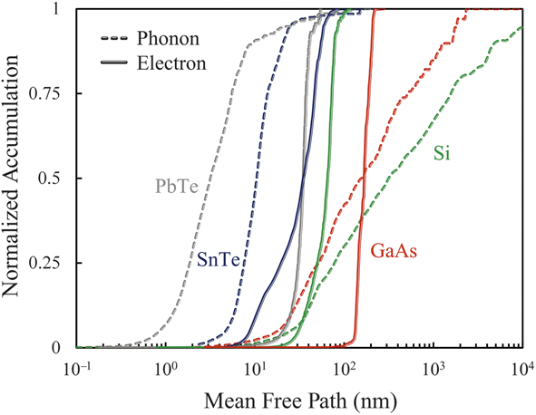
Ideally, one would design nanostructures such as grain size to be in between electron and phonon MFPs such that interfaces scatter more phonons than electrons. Knowing the MFP distributions of electrons and phonons in intrinsic materials is thus important. Although first-principles-based phonon simulation tools are becoming mature,Reference Esfarjani, Chen and Stokes10 electron simulation tools are just becoming available since the recent development of Wannier interpolation, a complete set of orthogonal functions used in solid-state physics, for electron–phonon coupling matrices.Reference Giustino, Cohen and Louie72,Reference Sjakste, Vast, Calandra and Mauri73 There are limited reports on fully first-principles-based simulations of electron thermoelectric transport properties, although simulations based on the constant relaxation time approximation are routinely reported.Reference Sun, Shuai, Ren and Singh74 In Figure 2, we compare electron and phonon MFP distributions in several representative materials.Reference Tian, Garg, Esfarjani, Shiga, Shiomi and Chen66,Reference Liu, Zhou, Liao, Singh and Chen75–Reference Song, Liu, Zhou, Ding and Chen79 More detailed studies show that nanostructures can also be effective for manipulating phonon and electron transport in some materials even when they are comparable to both the electron and phonon MFPs, since some long MFP electrons are disadvantageous to the Seebeck coefficient.Reference Minnich, Dresselhaus, Ren and Chen15
Normalized accumulation of thermal (dashed) and electrical conductivity (solid lines) for four representative materials. The blue, red, green, and gray lines represent the mean free path (MFP) spectra of SnTe,Reference Liu, Zhou, Li, Ding, Song, Liao, Fu and Chen78 GaAs,Reference Qiu, Tian, Vallabhaneni, Liao, Mendoza, Restrepo, Ruan and Chen76,Reference Luo, Garg, Shiomi, Esfarjani and Chen77 Si,Reference Esfarjani, Chen and Stokes10 and PbTe,Reference Tian, Garg, Esfarjani, Shiga, Shiomi and Chen66,Reference Song, Liu, Zhou, Ding and Chen79 respectively. The electrical conductivities are calculated at an n-type carrier concentration of 1 × 10²⁰, 1 × 10¹³, 1 × 10¹⁴, and 1 × 1017 cm–3 for SnTe, GaAs, Si, and PbTe, respectively. The differences between phonon and electron MFPs provide the possibility to independently manipulate their transport behavior.

First-principles simulation of defects scattering of phonons and electrons
Defects clearly affect phonon thermal conductivity; however, interpretations of experimental data to date are based on phenomenological models pioneered by Klemens and Callaway.Reference Klemens67,Reference Callaway68 Classical models, for example, cannot explain the interface resistance.Reference Swartz and Pohl80 Progress has been made in simulating interfacial thermal resistance based on the nonequilibrium atomic Green’s function and molecular dynamics.Reference Minnich44,Reference Tian, Esfarjani and Chen81 Simulations show that even atomic-point defects cannot be well described by Rayleigh scattering except in the long phonon wavelength range. For electron transport, critical questions remain about the charging states of these defects and how they contribute to carriers, as they can donate or trap mobile carriers.Reference Seebauer and Kratzer82 Knowing the charging states will enable answering the next question—how do these defects scatter electrons? Despite past studies on electrons in electronics and photonics, the current tools are far from being able to treat electron defect scattering on a first-principles basis.
Multiscale simulation of hierarchical defects
Although progress is being made on treating individual defects, putting them together to simulate realistic materials with hierarchical defects remains a major challenge. Appropriate methods to average the individual defect’s contribution and to bridge the scales are yet to be developed.
Conclusions and outlook
In this article, we summarized the formation conditions and phonon-scattering mechanisms of nano-microstructural defects in bulk thermoelectric materials, ranging from point defects to volume defects. The role of all-scale hierarchical nano-microstructures on impeding phonon transport is highlighted. We also discussed the main challenges for the roles of defects or microstructure from the perspective of simulations.
The thermal stability of nonequilibrium defects may become a critical issue during long-term practical applications. In addition to phonon engineering by defects, it is essential to pay attention to the effects of carrier concentration and carrier-scattering mechanisms,Reference Mao, Wu, Song, Shuai, Liu, Pei and Ren83,Reference Liu, Mao, Peng, Zhou, Gao, Sui, Pei and Ren84 which may counteract the beneficial contributions of the phonon portion and even deteriorate the final ZT. Therefore, delicate manipulation of the nano-microstructure to construct highly ordered hierarchical structures would provide a greater possibility of simultaneously optimizing electrical and thermal properties, which would open the path toward the realization of developing high-performance thermoelectric materials.
Acknowledgments
This work was supported by the “Solid-State Solar-Thermal Energy Conversion Center (S3TEC),” an Energy Frontier Research Center funded by the US Department of Energy, Office of Science, Office of Basic Energy Science, under Award No. DE-SC0001299.

Zihang Liu is a postdoctoral fellow in the Department of Physics and TcSUH (Texas Center for Superconductivity) at the University of Houston. He received his bachelor’s degree from Inner Mongolia University of Technology, China, in 2012. He obtained his PhD degree from Harbin Institute of Technology, China, in March 2017. His current research interests focus on nanostructured thermoelectric materials and devices. Liu can be reached by email at zliu48@central.uh.edu.

Jun Mao is a doctoral candidate in the Department of Mechanical Engineering at the University of Houston. He received his bachelor’s degree and his master’s degree in thermal and power engineering at Northeastern University, China. His current research mainly focuses on identifying novel thermoelectric materials. Mao can be reached by email at jmao5@uh.edu.

Te-Huan Liu is a postdoctoral associate in the Department of Mechanical Engineering at Massachusetts Institute of Technology (MIT). He received his BS degree in 2006 from National Central University, Taiwan, and PhD degree in 2012 from National Taiwan University, Taiwan. He has been a member of MIT’s NanoEngineering Group since 2015. His research interests include carrier transport in thermoelectric materials, electron–phonon interactions, and molecular dynamics simulations. Liu can be reached by email at thliu@mit.edu.

Gang Chen is the head of the Department of Mechanical Engineering and Carl Richard Soderberg Professor of Power Engineering at Massachusetts Institute of Technology (MIT). He is also the director of the Solid-State Solar-Thermal Energy Conversion Center. He obtained his bachelor’s and master’s degrees from Huazhong University of Science and Technology, China, and his PhD degree from the Mechanical Engineering Department, University of California, Berkeley, in 1993. He was an assistant professor at Duke University and then a tenured associate professor at the University of California, Los Angeles, before moving to MIT. His awards include the NSF Young Investigator Award, an R&D 100 Award, and an ASME Heat Transfer Memorial Award. He is a Fellow of AAAS, APS, and ASME. In 2010, he was elected a member of the US National Academy of Engineering. Chen can be reached by phone at 617-253-3523 or by email at gchen2@mit.edu.

Zhifeng Ren is an M.D. Anderson Chair Professor in the Department of Physics and the Texas Center for Superconductivity at the University of Houston. He is experienced in materials synthesis, physics, and applications and has made seminal contributions to high-temperature superconductors; carbon nanotubes; ZnO nanowires; thermoelectric materials; nanobiomaterials and sensors; flexible transparent electrodes; hydrogen, oxygen evolution reactions, and water splitting; a 2D nanosheets for enhanced oil recovery. He has published approximately 400 journal papers and has 38 issued patents. He received and 2008 R&D 100 Award and the 2014 Edith and Peter O’Donnell Award from The Academy of Medicine, Engineering & Science of Texas. He is Fellow of APS, AAAS, and NAI. Ren can be reached by phone at 713-743-8217 or by email at zren@uh.edu.