Introduction to piezo MEMS printing
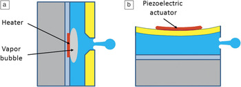
This article covers recent progress on the fabrication of epitaxial piezoelectric thin films. The crystalline quality of these epitaxial thin films is such that optimal piezoelectric properties with long-term stability can be obtained. This is important for many piezoelectric applications, such as piezoelectric inkjet printing. Inkjet print heads represented 15% of a US$10 billion microelectromechanical systems (MEMS) market in 2011.1 While thermal print heads, mostly for small office/home office (SOHO), have currently the major share of the MEMS inkjet market because they enable complementary metal oxide semiconductor compatible manufacturing, piezoelectric print heads are an emerging product in the professional printing arena. When comparing the two printing (droplet generation, see Figure 1) principles—thermal versus piezoelectric—the major advantage of the former, which is often decisive for the final product, is an extremely low price-per-nozzle combined with very high integration density (high dot-per-inch resolution). This makes thermal inkjet (TIJ) devices with throwaway print heads very attractive for SOHO and the low-end professional printing markets. However, thermal inkjets impose very stringent demands on the ink due to the fundamental limitation of the droplet formation process, which requires explosive liquid evaporation to create pressure in the print head for ink ejection. Therefore, TIJ print heads can only operate with water-based inks with a rather limited viscosity and temperature range.
Principle of (a) a thermal bubble jet print head and (b) a piezoelectrically actuated inkjet print head. Thermal print heads have currently the major share in the microelectromechanical inkjet market for use in small office/home office printers, while piezoelectric print heads are an emerging product in the professional printing arena.

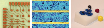
In contrast, the piezoelectric inkjet (PIJ) (see Figure 1b), which utilizes pure mechanical pressure created by the piezoelectric element, though more expensive, is able to jet a wide range of fluids over an extended temperature region. This universality makes PIJ an attractive tool not only for the high-end professional market, but also paves the way for industrial printing (e.g., electronics, 3D prototyping, bio- and medical printing) (see Figure 2). Additionally, PIJ print heads are more reliable and robust due to the possibility of early nozzle failure detection by using the piezoelectric actuator as a sensor while idle.Reference Groninger, Kruijt, Reinten, Schippers and Simons2, Reference Kwon and Kim3
Examples (from Reference 84) of industrial printing applications of piezoelectric inkjet (left to right): printed circuit board inner layer, solar cell front side metallization, and 3D printed wheels.

As mentioned previously, the disadvantage of PIJ is its high cost price. Until recently, PIJ print heads were manufactured using bulk Pb(Zr,Ti)O3(PZT) ceramics as the piezoelectric material in conjunction with micromachining. Scaling up of the thin PZT film deposition process to a 150–200 mm wafer diameter in combination with MEMS processing is a technology enabler for piezo-MEMS print heads with a drastically reduced price. As of today, two companies have introduced printing solutions containing piezo MEMS print heads. Additionally, several companies are considering the application of piezo-MEMS technology for manufacturing piezo-MEMS based print heads for the future.
Although the piezo-MEMS research area is almost two decades old and the integration of thin PZT films in MEMS devices is now an established procedure, reliable operation of such print heads suffers from a combination of several challenging problems, such as actuator stability. Such actuator behavior is the result of instability in the domain state of the film and has a dramatic impact on droplet size and speed during printing, eventually resulting in pixel displacement in the final image. This type of actuator deflection behavior can be explained by the presence of two contributions to the piezoelectric response: intrinsic contributions originating from the stretching/contracting of the unit cell dipoles in the piezoelectric material and extrinsic contributions, mainly attributed to domain wall movement.Reference Damjanovic4 The deflection decrease was attributed to a change in the domain state, such that after a few actuation cycles, extrinsic contributions and/or re-poling strains no longer contributed.
This effect can be completely eliminated by a thermal poling procedure,Reference Kohli, Seifert and Muralt5 which utilizes thermal energy in combination with an electric field to align defect dipole complexes to create an internal electric field aligned with the polarization direction and lock in the domain configuration—an effect known as imprint. It is worthwhile noting that this effect is extremely undesirable in ferroelectric random access memory (FeRAM) devices, while being imperative for proper operation of MEMS actuator devices. Unfortunately, the success of the thermal poling procedure is directly related to the quality and purity of the PZT layer and can be overshadowed by time dependent dielectric breakdown (TDDB) and subsequent catastrophic device failure. Several groups have attributed TDDB to field-driven redistribution of thermally activated oxygen vacancies in the film, resulting in the formation of a forward-biased p–n junction.Reference Desu and Yoo6–Reference Baiatu, Waser and Hardtl8
There are several methods to reduce the effect of the high defect concentration in PZT films by doping and/or by using oxide electrodes. However, this would only release some pressure on the poling procedure without rendering it unnecessary. Additional progress can be made by removing the poling procedure from the device manufacturing process.
Epitaxial PZT films provide a solution to these issues as, given the right choice of electrodes and deposition method, it can be shown that these films are intrinsically stable without the need for the poling process. In this article, we focus on Pb(Zr,Ti)O3thin films and in particular on efforts to obtain oriented/epitaxial layers for MEMS applications.
Epitaxial PZT films for MEMS
Among ferroelectric and piezoelectric materials, the perovskite solid solution Pb(Zr,Ti)O3 (PZT) is one of the most prominent compounds given its high electromechanical coupling, large piezoelectric coefficients, and reversible remanent polarization.Reference Shirane and Suzuki9 PZT has piezoelectric coefficients, which relate the mechanical strain produced by an applied electric field or vice versa, that are more than one order of magnitude larger than those of commonly used piezoelectric materials such as ZnO and quartz.Reference Polla and Francis10 The large piezoelectric response for compositions near Pb(Zr0.52Ti0.48)O3 rests on the presence of a transition region in the composition phase diagram, called the morphotropic phase boundary,Reference Jaffe, Roth and Marzullo11 where the crystalline structure changes abruptly. For PZT, this occurs when the tetragonal ferroelectric PbTiO3 mixes in a ∼1:1 ratio with the orthorhombic antiferroelectric PbZrO3.Reference Noheda, Cox, Shirane, Gonzalo, Cross and Park12, Reference Guo, Cross, Park, Noheda, Cox and Shirane13
In its polycrystalline form, this material is widely used for various applications, such as infrared sensors, ultrasound transducers, and scanning probe tubes.Reference Schwartz, Ballato, Heartling and Buchanan14, Reference Takayama and Tomita15 In the 1980s, development of thin-film deposition and characterization techniques prompted a technology push for the fabrication of thin-film-based devices, such as FeRAM.Reference Scott and Araujo16 In parallel, fundamental understanding of the physical properties of PZT and other ferroelectrics progressed in part as the result of the availability of epitaxial thin films.Reference Tybell, Ahn and Triscone17–Reference Vrejoiu, Le Rhun, Pintilie, Hesse, Alexe and Gosele20
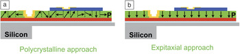
Epitaxial films provide a well-defined polar axis orientation (see Figure 3), as well as high density and compositional uniformity. These are essential to the increases in piezoelectric coefficients.Reference Muralt, Polcawich and Trolier-Mckinstry21 Compared to randomly oriented ceramics, films can be thinner for an equivalent remanent polarization while requiring lower coercive voltages, hence lowering the operation voltage. This is certainly a clear advantage for mobile electronics applications such as FeRAMs, where power consumption is an issue.
Schematic side view of a cantilever structure with a ferroelectric layer. On a silicon wafer, a heterostructure made of different buffer layers (light blue), bottom (red) and top (blue) electrodes, and a ferroelectric (green) or piezoelectric layer is deposited. The polar axis (arrow) is oriented along a well-defined crystallographic axis. In polycrystalline layers (a), the orientation of the ferroelectric polarization P is random, while in textured/epitaxial films (b), the polarization is aligned uniformly across the layer.

These advances in thin-film fabrication have motivated the MEMS community to turn to ferroelectrics/piezoelectrics as the transducer layer.Reference Trolier-McKinstry and Muralt22, Reference Muralt23 By utilizing the high piezoelectric response, large-displacement actuators as well as high-sensitivity sensors can be realized. Recently, Baek et al.Reference Baek, Park, Kim, Aksyuk, Das, Bu, Felker, Lettieri, Vaithyanathan, Bharadwaja, Bassiri-Gharb, Chen, Sun, Folkman, Jang, Kreft, Streiffer, Ramesh, Pan, Trolier-McKinstry, Schlom, Rzchowski, Blick and Eom24 reported the realization of piezo MEMS based on layers of Pb(Mg1/3Nb2/3)O3-PbTiO3, which possesses an extremely high piezoelectric coefficient due to engineered domain states in this relaxor ferroelectric material.
For x > 0.5, Pb(Zr1–xTix)O3 is a tetragonal perovskite with the ferroelectric dipole oriented along the long c-axis, whereas for 0.1 < x < 0.5, it becomes rhombohedral. Near the morphotropic phase boundary (MPB) for x ∼ 0.5, PZT is considered to be monoclinic. This lower symmetry phase acts as a structural bridge between the tetragonal and rhombohedral phases. The electrical and electromechanical properties (piezoelectric coefficients dij, dielectric constant εij where i and j refer to crystallographic orientations for the applied electric field, and the resulting elastic deformation or dielectric response, respectively) are strongly dependent on the orientation of the applied electric field with respect to the crystallographic axes. Hence, the integration of high-quality, highly oriented, and/or epitaxial piezoelectric layers in single-crystal form promises better performance for devices. Moreover, as applications are moving toward smaller, nanoscale devices, such as nanoelectromechanical systems (NEMS), uniformity of the piezoelectric response over nanometer length scales is required. This may limit the use of polycrystalline films due to their microstructural inhomogeneities, which will eventually compromise their performance. The fields of application of this new generation of devices will be sensors (e.g., microbalances), actuators (e.g., piezo-MEMS print heads, piezo cantilevers for atomic force microscopy), and energy harvesters (for the conversion of vibrational energy into electrical energy). Indeed, the development of high-sensitivity mass sensors is in rapid expansion, driven by the quest for the detection of very small masses. High-performance energy harvesting devices have also attracted much interest as small-scale sources of energy capable of powering micro-devices such as wireless sensor networks or monitoring systems for biomedical or environmental applications.Reference Jeon, Sood, Jeong and Kim25–Reference Shin, Lee, Park, Park and Lee33
Orientation dependence of Pb(Zr, Ti)O3 film properties on single-crystal substrates
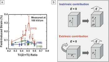
The piezoelectric response of oxide crystals is known to depend strongly on their orientation.Reference Park and Shrout34 One straightforward approach to control the orientation of Pb(Zr,Ti)O3 films is their growth on single-crystal substrates with a specific crystalline orientation. In addition, by selecting the lattice constant and thermal expansion coefficient of the substrate, the polar-axis orientation of Pb(Zr,Ti)O3 can be also controlled.Reference Utsugi, Fujisawa, Ikariyama, Yasui, Nakaki, Yamada, Ishikawa, Matsushima, Morioka and Funakubo35–Reference Utsugi, Fujisawa, Ehara, Yamada, Matsushima and Funakubo37Figure 4 shows the orientation dependence of piezoelectric and ferroelectric properties for a series of 2-μm-thick Pb(Zr0.5Ti0.5)O3 films prepared by pulsed-metalorganic chemical vapor deposition on (100)-, (110)-, and (111)-oriented SrTiO3 single-crystal substrates buffered with a layer of metallic SrRuO3 used as the bottom electrode.Reference Eom, Cava, Fleming, Phillips, van Dover, Marshall, Hsu, Krajewski and Peck38 The composition of the films sits at the MPB, and the resulting phase consists of a mixture of tetragonal and rhombohedral symmetries regardless of the film orientation.Reference Yokoyama, Honda, Morioka, Oikawa, Funakubo, Iijima, Matsuda and Saito39, Reference Yokoyama, Honda, Morioka, Okamoto, Funakubo, Iijima, Matsuda, Saito, Yamamoto, Okino, Sakata and Kimura40 This coexistence is preserved up to the Curie temperature of about 400°C. Compared to single-phase tetragonal or rhombohedral films, the mixed-phase films show larger orientation dependence of the various properties such as polarization, dielectric constant, and piezoelectric coefficient.
The piezoelectric response of epitaxial Pb(Zr, Ti)O3 films is known to depend strongly on their crystalline orientation.Reference Park and Shrout34 Such orientation is typically controlled by growth on single-crystal substrates with a specific crystalline orientation. (a) The field-induced strain is shown as a function of the Ti/(Zr+Ti) ratio for Pb(Zr,Ti)O3 films with (100) (blue circles), (110) (green squares), and (111) (red triangles) orientations consisting of tetragonal, rhombohedral, and mixed phases. (b) The intrinsic and extrinsic contributions to the piezoelectric response are schematically drawn. An electric field will enhance the polarization (ΔP s) due to the relative ion/cation shift (intrinsic) and rotation of the polarization (extrinsic) due to domain wall motion. Both contributions result in a larger polarization. Note: E, electric field; P s, saturation polarization; ΔP s, change in polarization under the application of an electric field.

As mentioned previously, the piezoelectric (and dielectric) response in ferroelectrics is due to two contributions:Reference Cross41 an intrinsic contribution based on the responses of the individual domains, and an extrinsic contribution from domain wall motion (see Figure 4b).Reference Fu and Cohen42 For Pb(Zr,Ti)O3, the enhancement of the dielectric and piezoelectric response near the MPB composition can be related to the contribution of not only intrinsic but also extrinsic effects.Reference Kim, Maria, Kingon and Streiffer43 These data clearly indicate that orientation control is one of the key issues to the realization of a large piezoelectric response in PZT films. It must be noted that which epitaxial orientation is best is currently under investigation because the piezoelectric response of the {100} orientation is larger than that of {111} for fiber textured PZT on Si substrates.Reference Muralt44
Epitaxial ferroelectric thin films on silicon
As silicon is the modern technological platform for both microelectronic devices and MEMS, a fundamental requirement for the realization of epitaxial piezoelectric MEMS (epi-piezo MEMS) is the integration of the functional piezoelectric layer on silicon wafers. Till the beginning of this century, the availability of epitaxial piezoelectric thin films on silicon has been limited by the hurdles related to the stability of the interface between oxides and silicon.Reference Reiner, Kolpak, Segal, Garrity, Ismail-Beigi, Ahn and Walker45 Due to the surface reactivity of silicon, the formation of an amorphous silica layer is a major roadblock to the achievement of a sharp and chemically stable Si/oxide interface. Moreover, the difference in lattice parameters and thermal expansion coefficients between silicon and oxide ferroelectrics represents an extra challenge for the growth of epitaxial thin films. For lead-based ferroelectrics-silicon heterostructures, an additional difficulty derives from Pb cation interdiffusion into the silicon substrate during the growth stage at high temperatures. Such diffusion results in a lead-deficient oxide layer and hence often leads to the formation of pyrochlore/fluorite phases (which are not ferroelectric), with a detrimental effect on the performance of the final devices.Reference Shirane and Suzuki9, Reference Shin, Park, Choi, Choi and Lee46–Reference Revesz, Li, Szabo, Mayer, Caudillo and Myers48
For these reasons, the strategy for integration of epitaxial ferroelectric thin films on silicon rests on suitable buffer layers that act simultaneously as structural templates and barriers for cation migration.Reference Sharma, Narayan, Jin, Kvit, Chattopadhyay and Lee49–Reference Moona, Ishiwaraa, Tokumitsua and Yoshimoto55
In the late 1980s, different teams actively pursued a process for the deposition of epitaxial oxide layers on Si. Ihara and co-workersReference Ihara, Arimoto, Jifuku, Kimura, Kodama, Yamawaki and Yamaoka56 investigated the growth of spinel MgAl2O4 on silicon. Following this work, MatsubaraReference Matsubara57 was able to integrate the perovskite PbTiO3 on silicon by using an MgAl2O4 thin film as a buffer layer. In 1989, the growth of yttria (Y2O3) films on Si(100) and of Y2O3:ZrO2 on Si(111) substrates by vacuum evaporation was also demonstrated.Reference Fukumoto, Fukumoto, Imura and Osaka58 This work formed the basis of double buffer layers such as CeO2/Y2O3:ZrO2 (CeO2/YSZ). In such stacks, which can be grown by pulsed laser deposition, the YSZ is able to scavenge the native silicon dioxide on the substrate surface,Reference Wang, Ong, You and Xu59 while CeO2accommodates the in-plane lattice mismatch with the active ferroelectric perovskite layer. Using these buffer layers, several groups have been able to grow PZT epitaxially on Si.
Yttria-stabilized zirconia/ceria buffer layers
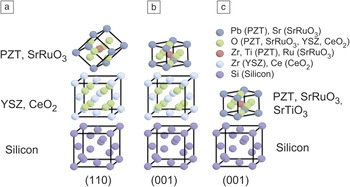
Indeed, yttria-stabilized zirconium oxide (YSZ), with the fluorite crystal structure, grows epitaxially on silicon. With the help of CeO2 as a second buffer layer, the in-plane epitaxial strain between the YSZ layer and the pseudo-cubic SrRuO3 is reduced to 2.2%, for cube-on-cube growth, if the perovskite cube is rotated by 45° (see Figure 5).
Schematic view of the epitaxial growth of lead zirconate titanate (PZT) on silicon. (a) <110> and (b) <001> PZT and SrRuO3 on YSZ/CeO2 (001) buffered silicon. (c) <001> PZT and SrRuO3 on SrTiO3 buffered silicon. The crystalline orientation of epitaxial Pb(Zr,Ti)O3can be controlled by appropriate buffer layers on silicon. Although different buffer layers are used in (b) and (c), the crystalline orientation of the PZT is the same. Note: YSZ, yttria-stabilized zirconia.

It is well-known that the performance of a ferroelectric capacitor is strongly influenced by the electrode material since it affects, among other things, leakage current, dielectric properties, as well as the growth and crystalline structure of ferroelectric films.Reference Lee, Thio and Desu60, Reference Jiang, Scott, Dawber and Wang61 To overcome the problem of fatigue, conducting-oxide electrodes such as RuO2,Reference Law, Tong, Li, Li and Poon62 SrRuO3 (SRO),Reference Eom, van Dover, Phillips, Werder, Marshall, Chen, Cava, Fleming and Fork63 LaNiO3,Reference Chen, Wu and Wu64 and (La,Sr)CoO3Reference Lee, Choi, Park, Noh and Lee65 have been used in PZT devices.
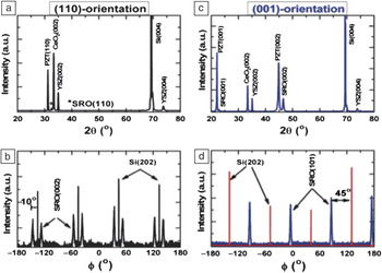
Appropriate tailoring of growth conditions can control the crystalline properties of the SrRuO3 electrodes and PZT capacitors. Figure 6a shows room-temperature x-ray diffraction (XRD) profiles of PZT/SrRuO3 films on CeO2/YSZ/Si when SrRuO3 is grown under normal conditions (in this case pulsed laser deposition at 600°C, 13 Pascal). The epitaxial relationship between the buffer layers and silicon is CeO2(001)‖YSZ(001)‖Si(001), as expected. However, the perovskite layers grow (110)-oriented, resulting in the structure PZT(110)‖ SrRuO3(110)‖CeO2(001)‖YSZ(001)‖Si(001) (as schematically shown in Figure 5a). In-plane XRD analysis of this sample (shown in Figure 6b) reveals four identical sets of two peaks (SrRuO3(002) reflections) positioned around the Si reflections (Si(202) orientation). This indicates that twin domains exist in the thin film.Reference Hou, Kwo, Watts, Cheng and Fork66 Although CeO2 is used as a second buffer layer, SrRuO3<111>‖YSZ/Si<110> in-plane epitaxy is still preferred. If a thin SrRuO3 layer (∼4 Å, one unit cell) is deposited at a high temperature (800°C) and in a reducing O2 environment (<10–4 Pascal), the epitaxial relation is modified. The deposition conditions favor the re-evaporation of Ru and the formation of a SrO layer, which then acts as a basal plane for the perovskite block. Successive growth of SrRuO3 at 600°C results in (001)-oriented growth of the electrode and the PZT layer, as shown in Figure 6c. The ϕ-scans in Figure 6d reveal a 45° rotation of the SrRuO3(202) orientation compared to the Si(202) orientation. This proves that the unit cells of SrRuO3/PZT are rotated on the CeO2/YSZ/Si stack, as schematically drawn in Figure 5b.Reference Dekkers, Nguyen, Steenwelle, te Riele, Blank and Rijnders67
The crystalline orientation of epitaxial Pb(Zr,Ti)O3 can be controlled by appropriate buffer layers on silicon. Using x-ray diffraction (XRD), the orientation is determined on CeO2/YSZ buffered silicon wafers. Out-of-plane orientation is determined by θ–2θ scans of Pb(Zr,Ti)O3/SrRuO3 (PZT/SRO) thin films on CeO2(001)/YSZ(001)/Si(001): (a) PZT(110) and (c) PZT(001), while in-plane orientation is determined from XRD pole plots: ϕ-scan profiles of SRO(002) and Si(202) reflections of the (b) PZT(110) and (d) PZT(001) sample. Note: θ, incidence angle; ϕ, in-plane rotation angle.Reference Dekkers, Nguyen, Steenwelle, te Riele, Blank and Rijnders67

SrTiO3/SrO as a buffer layer
Driven by the search for high-k materials, where k is the dielectric constant, for field-effect transistors, a new route for the growth of perovskite layers on silicon was devised in the early 1990s. This solution avoids the formation of amorphous SiO2 by using alkaline earth metal oxides as buffer layers.Reference Mori and Ishiwara68 Specifically, McKee and co-workers stabilized the interface between silicon and the perovskite layer by the creation of an interfacial silicide layer (BaO, SrO, (Ba, Sr)O) because of the favorable oxidation kinetics of the alkaline earth metals and low temperatures necessary for epitaxial growth.Reference Hubbard and Schlom69 This process, implemented by molecular beam epitaxy (MBE) and assisted by in situ monitoring tools, such as reflection high- energy electron diffraction (RHEED), requires a complex multi-step procedure, where fixed amounts of the elemental materials have to be deposited on the silicon substrate.Reference Reiner, Kolpak, Segal, Garrity, Ismail-Beigi, Ahn and Walker45, Reference Lettieri, Haeni and Schlom70, Reference Reiner, Garrity, Walker, Ismail-Beigi and Ahn71 Starting from SrTiO3-buffered silicon wafers, different groups have reported on the growth of high-quality PZT layers using different deposition techniques.Reference Lin, Hong, Wood, Verevkin, Ahn, McKee, Walker and Specht72, Reference Kim, Eom, Nagarajan, Ouyang, Ramesh, Vaithyanathan and Schlom73
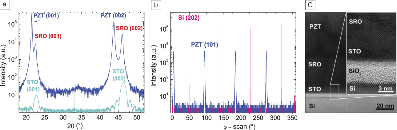
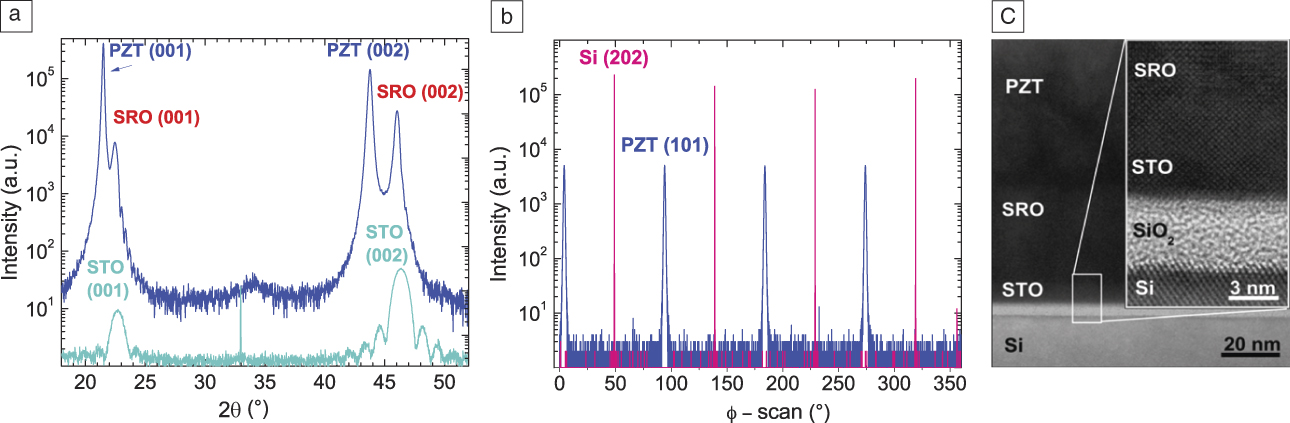
Using radio frequency-magnetron sputter deposition for the growth of SrRuO3/Pb(Zr0.2Ti0.8O3) epitaxial heterostructures on SrTiO3 buffered Si, Sambri et al. reported a remanent polarization of about 70 μC/cmReference Groninger, Kruijt, Reinten, Schippers and Simons2, with no significant leakage current up to 16 V and a d 33 piezoelectric coefficient (this value refers to the geometry where the electric field is applied along the ferroelectric polarization and the displacement is measured along this same axis) from the remanent response, measured by a piezoelectric force microscopy of 50 pm/V for a ferroelectric layer of 100 nm.Reference Sambri, Gariglio, Torres Pardo, Triscone, Stéphan, Reiner and Ahn74 Here, a 45° rotated cube-on-cube epitaxy of PZT on silicon is found, as schematically depicted in Figure 5c. Using XRD (see Figure 7), the following crystallographic relations are estimated: PZT [001]//SrRuO3[001]//SrTiO3[001]//Si[001] (out-of-plane) and PZT[100]//SrRuO3[100]//SrTiO3[100]//Si[110] (in-plane). A 4.5-nm-thick amorphous SiO2 layer appears at the interface between silicon and SrTiO3 after the growth of the buffer layer and does not affect the epitaxy of the stack, as confirmed by the cross-sectional high-resolution TEM picture in Figure 7.
(a) X-ray diffraction θ-2θ scan of the epitaxial heterostructure: Pb(Zr,Ti)O3 (100 nm)/SrRuO3 (30 nm)/SrTiO3 (6 nm)/Si. Finite-size oscillations around the Bragg peaks indicate the high crystalline coherence of the oxide layers. (b) Azimuthal φ-scan of the same heterostructure, confirming the epitaxy of Pb(Zr,Ti)O3 on silicon, achieved with cube-on-cube growth, with an in-plane rotation of 45°. (c) Cross-sectional transmission electron microscopy (TEM) image of the heterostructure revealing the presence of a 4.5-nm-thick amorphous SiO2 layer at the interface between silicon and the multilayer. Inset: high-resolution TEM picture showing the epitaxy of the oxide stack.Reference Sambri, Gariglio, Torres Pardo, Triscone, Stéphan, Reiner and Ahn74 Note: θ, incidence angle; ϕ, azimuthal angle; PZT, Pb(Zr,Ti)O3; SRO, SrRuO3; STO, SrTiO3.
Role of substrate clamping and strain
Since the PZT film is clamped to the substrate due to the crystalline relationship at the film/substrate interface, the piezoelectric response is influenced by the mechanical boundary conditions, in particular by clamping associated with the thick substrate.Reference Ouyang, Ramesh and Roytburd75–Reference Pérez de la Cruz, Joanni, Vilarinho and Kholkin77 The difference in crystal lattice parameters and/or the thermal expansion coefficient (TEC) mismatch between the substrate and the clamped thin film upon cooling will result in strain, often referred to as misfit strain (S M).Reference Janolin78 In epitaxial PZT films much thicker than the critical thickness (>80 nm), the lattice strain is completely relaxed,Reference Gariglio, Stucki, Triscone and Triscone79 and the remaining thermal strain is therefore either tensile or compressive depending on the choice of substrate.
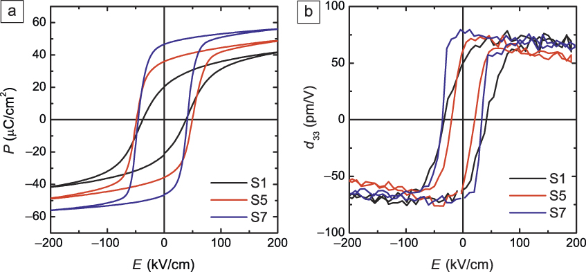
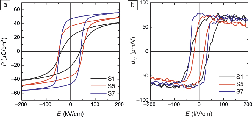
Epitaxial Pb(Zr0.52Ti0.48)O3 thin-film capacitors with SrRuO3 oxide electrodesReference Eom, Cava, Fleming, Phillips, van Dover, Marshall, Hsu, Krajewski and Peck80 on different substrates show substantially different ferroelectric characteristics. Figure 8a shows polarization (P) measurements as a function of electric field (E) (P-E loops) of epitaxial (001)-oriented PZT capacitors grown on different substrates. Table I shows that the misfit strain for these layers ranges from about +2 to –4 × 10⁻³. Films on Si substrates are under tensile strain because of the lower TEC of the substrate compared to PZT; conversely, the strain on oxide crystals is compressive due to the higher TEC. It is evident that films with high compressive strain show square and well-saturated hysteresis loops, while the films on silicon have more rounded and slanted hysteresis characteristics. In accordance with theoretical predictions, the average polarization in strained PZT films behaves as if it is neither completely out-of-plane nor completely in-plane.Reference Pertsev, Kukhar, Kohlstedt and Waser81 The measured out-of-plane polarization is highest for compressive strain (S M < 0) and lowest for tensile strain (S M > 0). However, whereas the residual polarization P r decreases, ε33 increases as the strain becomes higher.Reference Pertsev, Kukhar, Kohlstedt and Waser81 However, the effective piezoelectric response d 33,eff is rather independent of strain (Figure 8b).Reference Nguyen, Dekkers, Houwman, Steenwelle, Wan, Roelofs, Schmitz-Kempen and Rijnders82 This, of course, is good news for applications, as the actuation and sensing capabilities of PZT in buffered-silicon MEMS are as good as PZT on oxide single crystal substrates.
The ferroelectric and piezoelectric response is influenced by the mechanical boundary conditions, in particular by clamping associated with the thick substrate.Reference Ouyang, Ramesh and Roytburd75–Reference Pérez de la Cruz, Joanni, Vilarinho and Kholkin77 Such effects result in strained films. In this figure, the (a) polarization and (b) piezoelectric hysteresis loops of PZT samples on different substrates (i.e., CeO2/YSZ buffered Si(001) [S1, black], on CeO2 buffered YSZ(001) [S5, red], and on SrTiO3(001) [S7, blue]) are shown for fields up to 200 kV/cm measured at 1 kHz. A clear dependence of the residual strain on the remanent polarization is observed, while the piezoelectric properties are strain independent. Note: P, polarization; E, electric field; d 33, piezoelectric coefficient.
Measured and calculated properties of lead zirconate titanate (PZT) samples on different substrates in the order of decreasing misfit strain.Reference Nguyen, Dekkers, Houwman, Steenwelle, Wan, Roelofs, Schmitz-Kempen and Rijnders82

a (Å) and c (Å), in-plane and out-of-plane lattice constants, respectively; S M, misfit strain; TEC, thermal expansion coefficient of the substrate; P r, out-of-plane polarization; P s, saturation polarization; ε33, dielectric constant; and d 33,eff, effective piezoelectric response. Note: YSZ, yttria-stabilized zirconia.
Intrinsic stability of PZT properties in relation to crystalline structure
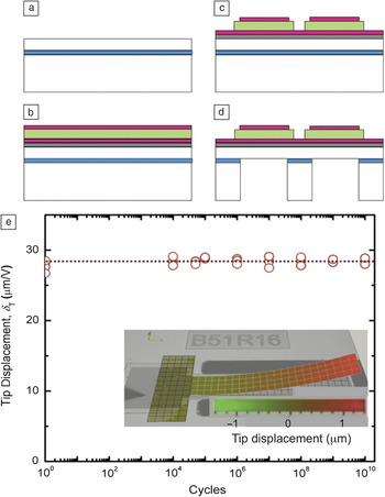
With respect to stability, epitaxial PZT outperforms textured films. Given the right choice of electrodes and deposition method, it is shown that epitaxial films are intrinsically stable. The long-term stability of epitaxial PZT also becomes evident in the actuation of MEMS devices. Silicon-on-insulator (SOI) wafers can be used to deposit epitaxial PZT and processed into MEMS structures. SOI technology refers to a layered silicon-insulator-silicon substrate in place of conventional silicon substrates, which are used in, for instance, microelectronics, to reduce parasitic device capacitance. SOI technology is also widely used in the fabrication of MEMS devices, where the top Si layer is typically used as the device layer, and the SiOx insulator as the etch stopping layer. Since the top Si layer is single crystalline with a perfect controlled orientation, epitaxial growth of PZT using the previously mentioned buffer layers can be reproducibly achieved. Figure 9a–d shows a typical process flow of the fabrication of membranes and cantilevers using wet chemical and dry etching techniques. Fabricated cantilevers show no fatigue and stable displacement for up to 1010 actuation cycles, as observed in Figure 9e.Reference Nguyen, Nazeer, Karakaya, Pham, Steenwelle, Dekkers, Abelmann, Blank and Rijnders83
Epitaxial PZT-based microelectromechanical systems (MEMS), such as membranes and cantilevers, are fabricated on silicon-on insulator (SOI) substrates using wet chemical and dry etching techniques. (a) MEMS fabrication process of epitaxial piezoelectric lead zirconate titanate (PZT) film on SOI substrates (white: silicon, blue: SiOx). (b) Deposition and (c) structuring of epitaxial PZT thin-film capacitors (red: SrRuO3 electrode, green: PZT), and (d) micromachining process. (e) Tip displacement as a function of the number of working cycles of a 400-μm-long cantilever (off-resonance). The inset shows a picture of a deflected cantilever based on epitaxial PZT MEMS. No fatigue and a stable displacement for up to 1010actuation cycles were observed.Reference Nguyen, Nazeer, Karakaya, Pham, Steenwelle, Dekkers, Abelmann, Blank and Rijnders83

Summary
We have reported on progress in lead zirconate titanate (PZT) thin-film deposition processes, which allow control of the crystalline orientation of oxide epitaxial heterostructures on silicon. For piezoelectric layers, this approach enables orienting the polar axis in a well-defined direction to maximize the electromechanical response. Ferroelectric and mechanical measurements of epitaxial PZT-based microelectromechanical systems (MEMS) show the potential of this approach: poling is no longer needed, and fatigue is strongly suppressed. Such epitaxial piezoelectric layers integrated in MEMS show enhanced performance and will enable reliable and stable operation in near-future piezo print heads.
Although the inkjet printing industry is maturing for PZT-based MEMS technology, current piezoelectric PZT thin-film technology and the use of “traditional” electrode materials such as Pt are already known to impair performance on the industrial scale, demanding novel material solutions, such as the use of epitaxial PZT thin films and epitaxial (oxide) electrode materials. Further developments, such as miniaturization down to the sub-micron scale, will put even tighter constraints on materials and processing, demanding new approaches and concepts. The rich variety of properties offered by epitaxial PZT will provide viable solutions as well as promising new functionalities. To achieve this, knowledge and know-how transfer of epitaxial PZT-based MEMS structures from basic research to industrial applications is required. This includes development of novel industrial scale fabrication processes for epitaxial PZT films and MEMS devices on industrial scale Si and silicon-on-insulator wafers (up to 200 mm).
Acknowledgments
H.F. acknowledges a grant from the Japan Society for the Promotion of Science (JSPS) through the Funding Program for World-Leading Innovative R&D on Science and Technology (FIRST Program), initiated by the Council for Science and Technology Policy (CSTP) and Ministry of Education, Culture, Sports, Science and Technology of Japan. T.Y. acknowledges a grant from the Japan Science and Technology Agency (JST) through the Precursory Research for Embryonic Science and Technology (PRESTO) program. A.S. and S.G. acknowledge support from the Swiss National Science Foundation through the National Center of Competence in Research “Materials with Novel Electronic Properties-MaNEP” and the EU Project Oxides. Discussions with P. Zubko are gratefully acknowledged. G.R., M.D., and I.S. acknowledge support from the Dutch government through the SmartMix programme. Discussions with M. Nguyen, E. Houwman, R. Steenwelle, and X. Wan are gratefully acknowledged.