I. INTRODUCTION
Since the development of the chemical vapor deposition (CVD) techniques for growing diamond thin and thick films, a wide range of cutting edge application areas, such as biological sensors, medical implants, infrared imaging technology, light/field emitter devices, heat sinks for electronic equipment, electrode materials, cutting tools, fusion plasma facing components, etc., have emerged for them.Reference Angus and Hayman1–Reference Porro, Temmerman, Lisgo, John, Villalpando, Zimmer, Johnson and Wilson8 Hot-filament CVD and microwave CVD are the most widely used techniques for growing diamond films. Uniform diamond coatings on large area substrates can easily be achieved with hot-filament CVD by maintaining high film uniformity compared to microwave CVD.Reference Porro, Temmerman, Lisgo, John, Villalpando, Zimmer, Johnson and Wilson8 A wide variety of diamond with different microstructures and morphology can be grown by varying the deposition conditions in CVD processes, and consequently, these variations affect growth rate and other properties as well.Reference Haubner and Lux9–Reference Haubner and Kalss11
Nucleation and growth of diamond films have been the subjects of numerous studies. Very comprehensive reviews have been published covering and analyzing the literature on diamond nucleation and growth.Reference Das and Singh12–Reference Liu and Dandy15 In these studies, the critical role of the substrate temperature or distance from filament assembly on diamond growth morphology has been stressed.
For adjusting diamond-coated tools and components to different applications, it is necessary not only to adapt diamond growth to substrate requirements but also to match diamond coating properties to application requirements to achieve high performance corresponding to the extreme properties of diamond.Reference Schäfer, Höfer and Kröger16
Multilayer diamond films may have useful applications in many engineering fields, e.g., in the areas requiring increased shock resistance. Takeuchi et al.Reference Takeuchi, Oda and Murakawa17 showed that in polycrystalline diamond film, due to crack propagation through the columnar particles, toughness of the film is decreased. The problem was overcome by applying bias current to the substrate repeatedly and intermittently while growing diamond film in hot-filament CVD.Reference Takeuchi, Oda and Murakawa17 As the result of varying bias, the continuity of columnar growth suppressed, which prevented crack propagation.Reference Takeuchi, Oda and Murakawa17
To our knowledge, in situ multilayer diamond growth, by changing substrate–filament distance with preoptimized respective substrate temperature, has not been studied before. The present study aims to grow multilayer diamond with hot-filament CVD for producing diamond films with enhanced mechanical properties by simply changing the substrate distance during deposition at constant filament power/temperature. To achieve this aim, the temperature-dependent growth morphologies of the films were defined, and then, multilayer diamond structures composed of layers with tunable thickness and morphology are grown just by bringing substrate closer to the filament assembly.
II. EXPERIMENTAL DETAILS
Polished p-type silicon substrates (2 × 2 cm, thickness ∼400 μm) with orientation (100) were ultrasonically agitated in diamond suspension (1:10) for the duration of 90 min (particle size 30–40 μm). The substrates were then ultrasonically cleaned in acetone for 10 min before placing them on a 2-cm-thick Mo plate, which was kept on cooled Cu holder. The details on the filament material and configuration are given in our previous work.Reference Ali and Qazi18 Diamond films were then grown with optimized parameters described below. During single layer deposition, two diamond films were produced separately at substrate temperatures of 740 and 780 °C, when the substrate distances were 8 and 7 mm from the filament assembly. Deposition time was set 270 min for 1st layer and 150 min for the 2nd layer. The deposition parameters for the three types of structures were first optimized. By using these parameters, the three films (1st layer: cauliflower structure, 2nd layer: pseudocubic structure, and 3rd layer: cubic structure) were then grown in a continuous sequence. In other words, all three films were produced in single experiment without removing film(s) from the deposition reactor. Substrate distance from filament assembly during 3rd layer was 6 mm, while its temperature was measured 830 °C and duration for deposition was 120 min. Due to narrow temperature ranges, substrate temperatures were carefully monitored. The substrate temperatures were recorded with a ±10 °C accuracy as measured with both B-type and K-type thermocouples, whereas the temperature of the filaments was kept 1900 °C in each experiment with a ±20 °C accuracy as measured with optical pyrometer (84 F, PYRO OPTICAL). The tips of the thermocouples were located in the center of the Mo disk exactly below the center of the substrates. For Raman spectroscopy measurement, the laser spot size was 100 μm and power on the sample was 10.3 mW.
After evacuation of the chamber, H2 (purity level: 4 N) gas was introduced, and after having pressure of 1.3 kPa (in 5 min), CH4 (purity level: 3 N) flow was started; the pressure was maintained at 5.3 kPa (in 15 min) throughout the deposition process. The flow rates of H2 and CH4 were adjusted by using mass flow controllers. Total flow rate was set to 200 sccm. The ratio of CH4was kept constant at 0.75%. Rotation speed of substrate was set 0.2 rpm. The mixed inlet gases passed over the filaments like a shower, and in this manner, flow direction of gases was perpendicular to filaments/substrate. The residence time was set 1004 s.
The films produced were characterized by scanning electron microscope (SEM) (JEOL, JSM-7000F, Japan) and μ-Raman spectroscopy (HR800 UV, Germany; 632.8 nm, He–Ne red laser).
III. RESULTS AND DISCUSSION
A. SEM Surface and fracture cross-sectional studies
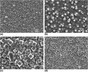
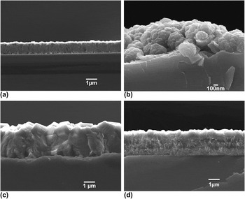
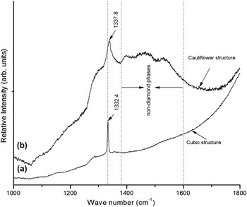
Diamond films grown at the lowest substrate temperature (740 °C) showed a typical cauliflower structure [Fig. 1(a)] as also conferred by other researchers, as, e.g., in Refs. Reference Zhang, Zimmer, Howe and Maboudian7 and Reference Haubner and Lux9. The reason of predominance of cauliflower diamond structure at lower substrate temperatures can be explained in terms of gas phase kinetic model suggested by Frenklach and Wang.Reference Frenklach and Wang19 The growth rate of this film was 0.25 μm/h as determined from its cross section [Fig. 2(a)]. The quality of both diamond films deposited with cauliflower and cubic structures were determined from the Raman spectra (Fig. 3). The diamond film with cauliflower structure has a high nondiamond content and intrinsic compressive stress indicated by the positive shift of Raman band of diamond.
SEM micrographs showing surface morphologies of diamond films deposited at substrate temperatures (a) 740 °C, (b) 780 °C, (c) 830 °C (x10 k), and (d) 830 °C (x5 k).

SEM interface micrographs showing (a) cauliflower (growth rate ∼0.25 μm/h), (b) formation of cubes on cauliflower (growth rate ∼0.27 μm/h), (c) well-faceted cubes (growth rate ∼0.4 μm/h), and (d) multilayer structures (1st layer: 4.5 h, ∼0.25 μm/h; 2nd layer: 2.5 h, ∼0.27 μm/h; 3rd layer: 2 h, ∼0.4 μm/h; total deposition time: 9 h, total growth rate ∼0.3 μm/h).

Raman spectra of (a) well-faceted cubic and (b) cauliflower diamond structures.

By bringing substrate closer to filament assembly from 8 to 7 mm, the substrate temperature increased from 740 to 780 °C. As a result of increased temperature, some of the grains of cauliflower structure partially transform into pseudocubic form [Fig. 1(b)]. Small crystalline clusters (cauliflowers) amalgamated into cubic form, as the substrate temperature increased, and enlarged them according to the size of the cauliflower, over which they reside and grow thereon [Fig. 2(b)].
Next, the substrate temperature was raised from 780 to 830 °C by reducing the substrate–filament distance from 7 to 6 mm. As a result, partially cubic morphology [Fig. 1(b)] merged into well-faceted cubic morphology [Figs. 1(c) and 1(d)] exhibiting crystalline aggregates with relatively small (100) facets (<1 μm) and uniform distribution. The growth rate in this case was higher (0.4 μm/h) compared with that at 780 °C, as determined from the fracture cross sections. The transformation of cauliflower structure to cubic can be explained by the enhanced surface diffusion with the increase of temperature and also higher dissociation of hydrogen atoms as proposed by Sokolov et al.Reference Skokov, Weiner and Frenklach20 By changing the substrate–filament distance and keeping filament power constant, the chemistry of the gas phase may change particularly the concentration of atomic hydrogen.
Formation of the cubic morphology requires planar growth,Reference Liu and Dandy15 which becomes possible with the elimination of nondiamond content in the film and the presence of appropriate atomic hydrogen on the growing diamond surface.Reference Ali and Ürgen21
Various studiesReference Clausing, Heatherly, Specht, More and Begun22–Reference Wild, Kohl, Herres, Müller-Sebert and Koidl35 have been presented on (100) orientation diamond films grown by hot-filament CVD and enlighten different point of view for having cubic morphology. As an example, Chen et al.Reference Chen, Yang and Lin23 observed that for (100)-oriented diamond films growth, additional process modifications, such as application of negative bias, are required. Zhang et al.Reference Zhang, Shi, Wang and Zhang24 concluded that under optimum growth conditions, (100) orientation improved with increasing deposition time. According to Yu and Flodström,Reference Yu and Flodström25 at higher pressure, diamond {100} is the favorable growth surface, whereas {111} is the favorable growth surface at lower pressure. Huang et al.Reference Huang, Yeh, Hwang and Chang26 grew (100)-oriented diamond films by a four-step process in hot-filament CVD system. Taher et al.Reference Taher, Schmidt, Naseem, Brown, Malshe and Nasrazadani27 reported that CH4 percentage is responsible for the change in morphology: “the increase in CH4 concentration resulted in two variations. The first was at 3 vol% CH4 where the (100) orientation became dominant at the surface instead of the mixed (111) and (100) orientations exhibited at 1 vol% CH4.” Zhang et al.Reference Shang, Fang, Liao and Cui28 reported that (100)-textured diamond films are due to manual scratching of Si substrates because using the same conditions and the pretreatment of 1 μm diamond powder suspension in acetone in an ultrasonic bath lead to non-(100)-textured diamond films. But in the present case, 30–40 μm diamond powder suspension in acetone in an ultrasonic bath leads to (100)-textured diamond films. Ma et al.Reference Ma, Wang, Liu, Su, Xu, Peng, Shi and Xia32 observed that a positive dc bias can increase the nucleation density and (100)-oriented growth in hot-filament CVD. Again, in the present work, neither the negative nor the positive substrate biases were used for achieving (100) orientation of diamond film. According to Wild et al.,Reference Wild, Kohl, Herres, Müller-Sebert and Koidl35 for {100}-oriented films, large values of alpha-parameter, α (e.g., α ≈ 2.5), result in a suppression of twin formation, whereas low values of α (e.g., α ≈ 1.5) lead to a deterioration in the film orientation and morphology due to twinning. Comparing the surface image shown in Fig. 1(d) with the published data, it appears that the best (100) orientation in hot-filament CVD has been achieved so far in this work.
In view of above, a question arises; then which parameter(s) is/are determining the diamond grain morphology. It is a well-established fact that changing hot-filament CVD process parameters allows modifying film morphology and texture of diamond film. The concentration of gaseous precursors at the growing diamond surface, and the temperature as well, can be tuned to grow {100} diamond films by hot-filament CVD and to affect the deposit’s phase purity and deposition rate. Such tailoring of process parameters depends on the specific design of the CVD reactor. Besides that, authors believe that presence of (100) orientation of diamond film may also be linked with the residence time,Reference Skokov, Weiner and Frenklach20, Reference Heimann, Raiko and Buck36 purity level of gases, rotation speed of substrate, and direction of gases flow. While varying the substrate/filament distance, affect of [H] at the surface of growing diamond may also account in the formation of pseudocubes and {100}-oriented cubes; Yarbrough et al.Reference Yarbrough, Tankala, Mecray and DebRoy37 stated that when the filament/substrate distance is varied, the concentration of [H] at the surface is changing and this has important effects on the temperature (exothermic recombination of [H] at the surface).
B. Kinetics and thermodynamics of diamond growth
This section presents a study of kinetics and thermodynamics of diamond growth versus variation in substrate distance. Thermodynamically artificially grown diamond is in a metastable phase, so enough driving force is required to put into effect constructive transformation. On the other hand, kinetics of diamond growth determines the rate, i.e., transition from unstable to stable state or between two stable states. So it involves energy barrier to terminate the transition. As several parameters affect the growth of diamond in CVD, it is rather complex to determine kinetics and thermodynamics of diamond growth.
According to Cheesman et al.,Reference Cheesman, Harvey and Ashfold38 the dominant process for carbon addition, in the form of methyl radicals, is predicted to be addition to a surface radical site, opening of the adjacent C–C dimer bond, insertion, and ultimate ring closure. Other steps such as insertion across the trough between rows of dimer bonds or addition to a neighboring dimer leading to formation of a reconstruction on the next layer may also contribute.
In early stages of the synthesis of diamond, clusters of carbon atoms are formed on the substrate surface. Due to thermal conditions, a change in the bonding structure occurs, which converts sp 1 to sp 2 and at a later stage into sp 3.Reference Singh39
During transformation in various structures, atomic/ionic rearrangements take place. As a result, new bonds are formed and nearby atoms are displaced, which lead in the transition from their equilibrium positions. So there is temporary increase in local energy, forming an activated state. Now, interatomic interaction plays important role in determining the system energy. The 3rd layer in Fig. 2, i.e., (100) orientation, is at lower free energy compared to the 2nd layer. Similarly, 2nd layer is at a lower free energy compared to the 1st layer. Because of this, the 1st layer tends to be converted into the 2nd layer and 2nd layer into the 3rd.
Variation in free energy of these three layers is a thermodynamic behavior, while activation energy is the maximum energy that separates these layers/equilibrium states. Thus, activation energy is a rate determining step, which is normally given in transition state. Surface energy depends on substrate temperature. As indicated in Fig. 2, by bringing substrate closer to the filament assembly, the temperature increases resulting in greater mobility of atoms/molecules and thus more chance (probability) for them to overcome the energy barrier.
As the substrate is brought closer to the filament assembly, thermal disassociation of hydrogen becomes higher, which can now effectively etch graphite growing along with diamond (graphite has a lower free energy compared to diamond). However, it is indicated from Fig. 2 (3rd layer) that [H] also acts as a catalyst, as it speeds up the reaction by decreasing the activation energy. Again, by bringing substrate nearer to the filament assembly, carbon-containing species exhibit higher kinetic energy and hence larger surface mobility on the surface of growing diamond film.
C. Raman spectra
From the Raman spectra, the band shifting to wave number lower or higher than natural diamond (1332.1 cm−1) indicates that the film is under stress (tensile or compressive).Reference LeGrice, Nemanich, Glass, Lee, Rudder, Markunas, Glass, Messier and Fujimori40 The residual stress (σ) value is calculated by σ (GPa) = −0.567 (v − v 0), where v 0 = 1332.1 cm−1 and v is the wave number of the diamond peak.Reference Kuo, Lin and Lien41 The “σ” calculated by above formula in diamond film having cauliflower structure is −3.23 GPa and for cubic morphology is −0.17 GPa. Raman spectra of the coating, occupied with well-faceted cubic crystals, consisted of a strong band at 1332.4 cm−1, close to natural diamond (1332.1 cm−1), indicating low intrinsic stress, and also almost free of nondiamond species demonstrating the good purity of the film [Fig. 3(a)]. This clearly indicates that film deposited at substrate temperature of 740 °C has higher level of compressive stress compared to film grown at substrate temperature of 830 °C but both films exhibit compressive stress as σ > 0. The higher value of compressive stress actually indicates poor quality of diamond. According to Prawer et al.,Reference Prawer, Nugent, Jamieson, Orwa, Bursill and Peng42sp 2-related grain boundary contributions arise from either disordered amorphous carbon (around 1380–1520 cm−1) or from nanosized grains-/tetra-polyacetylene-like fragments (around 1150–1250 cm−1), which are also visible in cauliflower structure spectrum of Fig. 3. Therefore, the Raman spectra of diamond film with cubic morphology reveal better purity compared to the diamond film deposited with cauliflower structure, which is also in-line with SEM investigations. On one side, cauliflower structure (of multilayer) is helpful in preventing crack propagation and annihilation of film. On the other hand, cubic morphology of diamond film with lower degree of stress is helpful in improving surface roughness and quality of the film.
D. Proposed application of multilayer diamond films
After determining temperature-dependent growth morphology, multilayer films were grown, simply, by changing the substrate distance from filament assembly. Growing of films was started with parameters for cauliflower growth, followed by partially (pseudo) cubic and then cubic growth for a total deposition period of 9 h [Fig. 2(d)]. The thickness of each layer showed correlation with the coating rates determined from the experiments with single layer coatings. Starting the coating process with suitable parameters for achieving structures possessing compressive stress [Fig. 3(b), cauliflower] and then growing cubic films on the transition layer (pseudocubic) are expected to increase the adhesion of the films to the substrate.
Base on the published work,Reference Schäfer, Höfer and Kröger16, Reference Takeuchi, Oda and Murakawa17 the present approach can be used for solving the adhesion problems of diamond coatings deposited not only on Si substrate but more likely on hard tool materials/substratesReference Sein, Ahmed, Jackson, Ali and Gracio5, Reference Salgueiredo, Almeida, Amaral, Fernandes, Costa, Silva and Oliveira6, Reference Porro, Temmerman, Lisgo, John, Villalpando, Zimmer, Johnson and Wilson8, Reference Köpf, Haubner and Lux10, Reference Haubner and Kalss11, Reference Huang, Yeh, Hwang and Chang26, Reference Taher, Schmidt, Naseem, Brown, Malshe and Nasrazadani27, Reference Chattopadhyay, Sarangi and Chattopadhyay43, Reference Amaral, Almeida, Fernandes, Costa, Oliveira and Silva44 along with extra advantage to have lower surface roughness of the top layer. The increase of performance of these diamond multilayers is largely due to reduced crack propagation. Multilayers of fine-grained and coarse-grained diamond have been developed,Reference Schäfer, Höfer and Kröger16 showing increased shock resistance due to reduced crack propagation. In another study, diamond secondary nuclei are grown on a substrate by applying bias current to the substrate repeatedly and intermittently; multilayer diamond films, in which the continuity of grain growth is suppressed, are synthesized,Reference Takeuchi, Oda and Murakawa17 but the procedure was complex and expensive.
Due to certain limitations, this study does not provide any demonstration that such procedure allows attaining better adhesion and/or resistance to crack propagation. But on the basis of Raman spectra and morphology results along with published literature, authors strongly believe that multilayer diamond growth, which is presented here, is useful, where smooth diamond surface, annihilating crack propagation, and increasing the adhesion are major challenges.
IV. CONCLUSIONS
In the present study, after determining the temperature-dependent growth morphology of the diamond film with respect to the substrate distance from filament assembly, multilayered diamond films were successfully grown with cubic morphology over cauliflower structure in a hot-filament CVD system. SEM micrographs showed that cubic morphology initiated on top of the cauliflower structure. By decreasing substrate distance 8 to 6 mm from filament assembly (in three steps), substrate temperature raised from 740 to 830 °C and cauliflower morphology merged into well-defined square grains with an increase in the growth rate. Raman spectroscopy studies conducted on the diamond films showed better quality of diamond film at higher substrate temperature. The internal stress type and magnitude showed dependence on the growth morphology. The cauliflower-structured film grown at lower substrate temperature possessed compressive stress, which decreased gradually by the increase in substrate temperature, i.e., by bringing substrate closer to the filament assembly. The lower value of “σ” in diamond film grown with cubic morphology confirms better purity within our experimental setup. The multilayer diamond structure is useful where improved adhesion, surface finish, and annihilating crack propagation are major concerns.
ACKNOWLEDGMENT
This work was supported by TÜBİTAK under 2216-Postdoctoral Fellowship Programme (Ref: B.02.1.TBT.0.06.01-216.01-677-6045).