Introduction: A brief history of graphene
Graphene has a long history. In the 1800s, graphite was known as a layered material that could be exfoliated by various methods. The famous chemist AchesonReference Acheson1 had developed exfoliation methods (that he called deflocculation) to produce colloidal suspensions of small graphitic flakes that he called “dags.” These colloidal graphite suspensions have been extensively used in the electronics industry as a conducting paint to produce conducting surfaces in vacuum tubes. In 1907, the material was described as follows: “The graphite is in what Mr. Acheson calls the ‘deflocculated’ condition, a condition of fineness beyond that attainable by mechanical means, a condition approaching the molecular slate.”Reference Acheson1 Indeed, these suspensions probably contained graphene flakes as Acheson suspected. He then found that coating metals with deflocculated graphite prevented corrosion.
But Acheson also discovered another material. He produced silicon carbide (SiC) that he called carborundum.Reference Acheson1 It was first used as an abrasive. He then found that upon heating SiC, silicon evaporated, leaving behind very pure graphite. Exfoliated graphite and graphite on SiC would become extremely important a century later for their electronic properties. It was later found that graphene layers form on SiC.
It is not well known that SiC (a wide bandgap semiconductor) was already incorporated in electronics since the early 1900s, when SiC crystals were used as diode detectors for radio receivers.Reference Dunwoody2 In fact, the first light-emitting diodes were produced using SiC at that time.Reference Round3 But the quality and size of the crystals left a lot to be desired. High-quality SiC crystals are now grown using the Lely process.Reference Lely4
In 1859, using nitric acid and potassium chromate, BrodieReference Brodie5 produced “graphitic oxide” consisting of graphene sheets with epoxide groups bridging adjacent carbon atoms. Immersing this material in water caused the individual layers to separate.
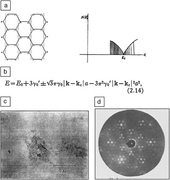
In 1962, BoehmReference Boehm, Clauss, Hofmann and Fischer6 recognized that graphite oxide monolayers could be reduced to graphene using hydrazine. He was able to measure the thicknesses of these graphene layers using a combination of surface measurements. Boehm thereby was the first to produce and to measure freely suspended graphene flakes (Figure 1). In 1982, Boehm officially coined the term “graphene,” which he saw as a macromolecule (the “ene” ending refers to hydrogen at the edges, as for example in benzene) (Figure 1).Reference Boehm, Setton and Stumpp7
The early days: (a) graphene structure and density of states calculated by Wallace (1947) using the tight binding model,Reference Wallace12 which showed the conical band structure; (b) equation recently renamed the “Dirac cone;” (c) electron micrograph of a graphene flake from Boehm (1962);Reference Boehm, Clauss, Hofmann and Fischer6 (d) low energy electron diffraction image of Si-face epitaxial graphene on SiC, by van Bommel (1972).Reference van Bommel, Crombeen and van Tooren8

In 1975, van Bommel et al.Reference van Bommel, Crombeen and van Tooren8 studied the graphitic layers that are formed when hexagonal SiC is heated in vacuum (Figure 1). They confirmed Acheson’s observation that the material graphitizes, because silicon sublimes from the crystal surfaces. However, they also noted that crystal faces graphitized differently. Graphite grown on the silicon-terminated face (Si-face) was clearly epitaxial (that is, aligned with the silicon substrate), while the carbon-terminated face (C-face) seemed to be rotationally disordered. Further studies by Forbeaux et al.Reference Forbeaux, Themlin and Debever9 in 1998 confirmed these results but also indicated that the graphite layers were essentially decoupled from the substrate, causing them to conclude that “layer by layer growth opens up the possibility of an isolated single graphene layer ‘floating’ above the substrate.”
Graphene has also been produced by other methods, including chemical vapor deposition of carbon-containing gases on various metals. The two-dimensional crystal properties were well known and intensely studied in the surface science community (for a review, see Gall et al.Reference Gall, RutKov and Tontegode10).
In 1999, Ruoff and co-workersReference Lu, Yu, Huang and Ruoff11 recognized that graphene might be important for various reasons, and they developed a mechanical method to exfoliate graphite. They etched vertical pillars in a graphite crystal and demonstrated that very thin graphite flakes could be mechanically slid off of the pillars (see Figure 2a). Their goal was to produce graphene sheets by this method.
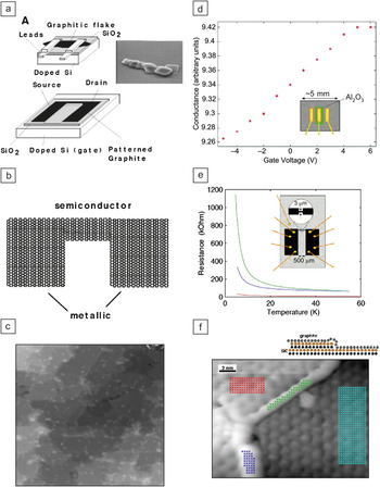
Developments of graphene-based electronics as documented in early proposals a, b, and c, in 2001, and d, e, and f, in 2003.Reference de Heer21 (a) Proposed field effect transistor composed of a thin graphite or graphene flake deposited on an oxidized degenerately doped silicon wafer. The flakes were to be produced using the Ruoff pillar methodReference Lu, Yu, Huang and Ruoff11 (inset). (b) Proposed graphene transistor with metallic graphene leads and a semiconducting graphene channel. (c) Early example of epitaxial graphene on the Si-face of a SiC chip. (d) Field effect on an unpatterned graphene sheet. (e) Patterned graphene ribbon resistance versus temperature. (f) Scanning transmission microscopy image of epitaxial graphene. Also reported were scanning tunneling spectroscopy results demonstrating that the graphene layer was continuous over the substrate steps. These data were published in 2004.Reference Berger, Song, Li, Li, Ogbazghi, Feng, Dai, Marchenkov, Conrad, First and de Heer23

The electronic properties of graphene have been well understood since 1947, when WallaceReference Wallace12 used simple tight-binding calculations to gauge its band structure (Figure 1). In 1960, McClureReference McClure13 calculated the properties of graphene in magnetic fields and demonstrated the unusual magnetic field dependence of the Landau levels. Others confirmed and expanded these calculations. In 1998, AndoReference Ando, Nakanishi and Saito14 recognized the equivalence of Wallace’s graphene band structure with the dispersion relation of a massless fermion (i.e., a neutrino), in which the spin was replaced by a pseudospin (that actually characterizes the bonding and antibonding character of the wave functions). He also recognized the resulting nontrivial Berry’s phase, a phase shift that affects the energy levels of electrons in graphene in magnetic fields, as revealed in magneto-transport measurements, such as the quantum Hall effect. Moreover, he predicted that the pseudospin character would be responsible for the reduction of backscattering both in nanotubes and in graphene.
The carbon nanotube connection
The ultimate demise of silicon electronics as the primary driving force of electronics innovation has been predicted for decades. This “end of Moore’s law” dilemma spurred research around the globe in the search for a viable alternative material. Carbon nanotubes had been discovered in the 1990s, and they were first seen primarily as interesting for their great mechanical strength; unusual early applications proposed elevators to space.
IijimaReference Iijima15 had pointed out that carbon nanotubes could be seen as rolled up graphene sheets, and Mintmire et al.Reference Mintmire, Dunlap and White16 observed that depending on their helicities, carbon nanotubes could be either metals or semiconductors. This very interesting observation suggested that nanotubes might be used for electronics. In 1998, my group demonstrated that carbon nanotubes are ballistic conductors,Reference Frank, Poncharal, Wang and Heer17 wherein electrons move large distances (order of microns) without scattering, which is very favorable for electronics. Independently and contemporaneously, White and TodorovReference White and Todorov18 provided a theoretical explanation for ballistic transport in carbon nanotubes.
That same year, Tans et al.Reference Tans, Verschueren and Dekker19 demonstrated the first nanotube transistor. It consisted of a nanotube with metal contacts on either end that was placed on an oxidized degenerately doped silicon wafer. This geometry allowed the nanotube to be “back gated:” applying a voltage to the silicon wafer induces charges on the nanotube, thereby turning it on and off. Nanotube transistors were remarkable, and over time, they demonstrated impressive characteristics. However, there remained a fatal flaw; while the nanotube resistance can be very low, for quantum mechanical reasons, the contact resistances are very high, on the order of 10 kΩ. Heat is dissipated at the contacts, making them extremely fragile. Besides the contact and interconnect problem, there are also problems with nanotube placement. Given the status quo of nanotube electronics research, it is clear that nanotube electronics will not replace silicon electronics in the foreseeable future, although specific nanotube devices, such as sensors and interconnects, may become commercially viable. In either case, a valuable lesson had been learned: carbon might play a role in future electronics, setting the stage for the next development.
The invention of graphene electronics
Because of the ever increasing interest in graphene in general, it is relevant to recount the early developments leading to the invention of graphene electronics for historical purposes. This documented account is meant to provide context to the invention.
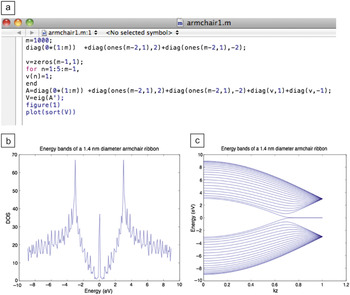
In early June 2001, a colleague called me and asked for a carbon nanotube tight binding program that I had written years earlier. I had lost the program and therefore started to rewrite it. It is very easy to write the program for finite ribbons or nanotubes. It involved a simple matrix with the rows and columns representing the carbon atoms. In the matrix, ones are placed whenever two carbon atoms are nearest neighbors and zeroes otherwise. A nanotube is simply a ribbon for which the two edges are connected. I first ran the program for a ribbon, and to my amazement, the resulting density of states resembled that of a nanotube, both with semiconducting and metallic varieties (Figure 3). A full band structure calculation confirmed this. (We later found that Nakada et al.Reference Nakada, Fujita, Dresselhaus and Dresselhaus20 had done similar calculations several years earlier.)
The tight binding calculations that resulted in graphene-based electronics in June 2001. (a) Simple finite graphene ribbon tight binding program. (b) Ribbon density of states. DOS, density of states. (c) Ribbon band structure. Standard nanotube nomenclature was used; armchair and zigzag interchanged in the graphene nomenclature.

This work showed that graphene ribbons were electronically similar to nanotubes, and I realized this was extremely important. For the next month, I expanded this idea and calculated the electronic properties of a great many structures, including rough edges, junctions, magnetic fields, and many other features. I developed a program that would allow any graphene structure to be drawn, after which the electronic structure would be calculated. It turns out that a “brick wall” topology (where the mortar lines represent bonds) is identical to that of graphene. This greatly simplifies the indexing of the atoms in graphene.Reference de Heer21
I also developed a program to propagate waves through finite graphene structures, which was easy since the wave functions could be exactly calculated. These calculations convinced me that graphene-based electronics was possible, and that the major hurdles in carbon nanotube–based electronics were potentially resolved. Specifically, wide ribbons (functioning as the metal leads) could be connected to a narrow ribbon (functioning as a semiconducting channel) to produce graphene transistors. Expanding on this theme, entire integrated structures could be developed simply by appropriately cutting a graphene sheet.Reference de Heer21
In July 2001, at the NT01 nanotube conference in Potsdam, Germany, I discussed graphene-based electronics with Robert Haddon, University of California Riverside, who was very interested because of the connection to his work on fullerenes and nanotubes. He contemplated the intriguing prospects of chemical functionalization of graphene and its edges. This is, of course, a very important aspect when one realizes that graphene is actually an organic macromolecule.
The next step was to assemble a research group to work on this project. Claire Berger and Phillip First, both at the Georgia Institute of Technology (GIT), were willing to participate. We then needed a viable platform. We became aware of the various graphene production methods mentioned previously and started work in three directions, as documented in our proposal to the National Science Foundation in 2001 (Figure 2a–c).Reference de Heer21
The first method described in the 2001 proposal involved an exfoliation method using Ruoff’s pillarsReference Lu, Yu, Huang and Ruoff11 to deposit graphene flakes on oxidized degenerately doped silicon wafers to make field effect transistors (Figure 2a), a predecessor to the method used by Novoselov et al.,Reference Novoselov, Geim, Morozov, Jiang, Zhang, Dubonos and Grigorieva22 from the University of Manchester, in their 2004 paper. We anticipated that this method would only be useful for proof of principle demonstrations. The second method involved the graphitization of SiC. At the time the proposal was submitted, Phil First had graphitized a few SiC samples in his UHV chamber to provide preliminary results (Figure 2c). The third method involved chemical vapor deposition growth on metals.
The 2001 proposalReference de Heer21 listed the following five important properties of graphene-based electronics:
• Size-tunable electronic bandgaps,
• Chemical robustness,
• Immunity to electromigration (a major problem in nanoelectronics),
• High current capability, and
• Electrically tunable conductivity using the field effect via a proximal gate electrode (“gate-doping”).
It concluded with this statement: “Our vision is nothing less than a new form of large-scale integrated electronics based on ultrathin films of lithographically patterned graphite.” Three of the items relate to the extreme stability of graphene, which indeed is the most stable macromolecule known.
This proposal was not funded, nor were three others that followed in 2002. Referees generally thought that graphene-based electronics were of little technological or scientific value. Graphene had been around for a long time, and it was mainly a nuisance, a poison for catalysts. From their reports, it was abundantly clear that only a demonstration would convince them.
In late 2002, we had the necessary demonstrations. We had successfully produced epitaxial graphene using van Bommel’s method and patterned it using e-beam lithography methods to make simple Hall bars and transport measurements, demonstrating the 2D gas properties of epitaxial graphene. We had also demonstrated top gating.Reference Berger, Song, Li, Li, Ogbazghi, Feng, Dai, Marchenkov, Conrad, First and de Heer23 Most of the transport measurements at that time were conducted at the mesoscopic science laboratories of the Neel Institute of the CNRS in Grenoble, France, which was and still is Claire Berger’s base institute.
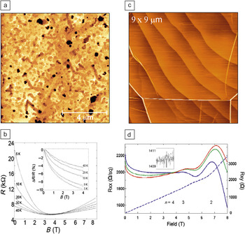
These data were compiled in a proposal to the NSF in June 2003 and published in 2004 (Figure 2d–f).Reference de Heer21, Reference Berger, Song, Li, Li, Ogbazghi, Feng, Dai, Marchenkov, Conrad, First and de Heer23 At that time, the mobilities (as determined from the magnetoresistance and Hall effectReference de Heer21, Reference Berger, Song, Li, Li, Ogbazghi, Feng, Dai, Marchenkov, Conrad, First and de Heer23) were not good, typically on the order of 15 cm2 V–1 s–1 (Figure 4b), and it was clear why. Atomic force microscopy (AFM) studies showed that the graphitized surfaces were pitted, resembling Swiss cheese (Figure 4a). Nevertheless, we contacted Intel Corp., who was very interested in our work and provided our first significant funding in September 2003. In June 2003, we also filed our first patent, which claimed the invention of graphene-based electronics, incorporating the concepts we had developed in the previous two years. The patent, signed by de Heer, Berger, and First, was issued in 2006.Reference de Heer21
Examples of epitaxial graphene and transport properties. (a) Atomic force microscopy (AFM) image of typical Swiss cheese morphology of graphene grown by the van Bommel method (in UHV). (b) Conductance (μS) versus magnetic field for UHV grown graphene Hall bar; the mobility is 15 cm2 V–1 s–1.Reference Berger, Song, Li, Li, Ogbazghi, Feng, Dai, Marchenkov, Conrad, First and de Heer23 (c) AFM of a typical furnace grown multilayer epitaxial graphene showing substrate steps and pleats on the graphene (note the absence of obvious defects). (d) Transport measurement of monolayer epitaxial graphene Hall bar on the Si-face, showing precursor behavior to the quantum Hall effect. Mobility is 1,100 cm2 V–1 s–1.Reference Berger, Song, Li, Li, Ogbazghi, Feng, Dai, Marchenkov, Conrad, First and de Heer23

The poor mobilities were of great concern and clearly linked to the production method. I started experimenting with alternative furnace methods and found that by confining the SiC samples in a graphite cylinder, the quality of the graphene dramatically improved. Mobilities exceeding 1000 cm2 V–1 s–1 were commonly achieved, and the AFM images revealed that the surfaces were now not pitted (Figure 4c). In summer 2004, we produced and measured a Hall bar (standard structure commonly used in electronics to determine transport properties of materials) on the Si-face with a mobility of about 1100 cm2 V–1 s–1 that exhibited large Shubnikov-de Haas oscillations (i.e., variations in resistance with applied magnetic field) and signatures of the quantum Hall effect (Figure 4d). At the time, it was difficult to measure the thickness of the layers accurately, so we relied on Auger electron spectroscopy. We were not aware that this method overestimates the graphene thickness, because it did not take into account the electrically inert carbon-rich buffer layer on the Si-face. Therefore, we thought that we were measuring an ultrathin graphite trilayer, while, in fact, it was a graphene monolayer. These measurements were the first graphene transport measurements.Reference Berger, Song, Li, Li, Ogbazghi, Feng, Dai, Marchenkov, Conrad, First and de Heer23–Reference de Heer, Berger, Wu, First, Conrad, Li, Li, Sprinkle, Hass, Sadowski, Potemski and Martinez25
We published these results in December 2004 in a paperReference Berger, Song, Li, Li, Ogbazghi, Feng, Dai, Marchenkov, Conrad, First and de Heer23 in which we presented, in detail, our vision for graphene-based electronics, and we showed extensive structural and electronic characterization of virgin and graphene samples patterned using microelectronics lithography methods. We had presented many of these results at the March meeting of the APS earlier that year (2004).Reference Berger, Song, Li, Li, Ogbazghi, Feng, Dai, Marchenkov, Conrad, First and de Heer23, Reference Berger, Song, Li, First, Bellisard and deHeer24
Beyond the monolayer: The discovery of multilayer epitaxial graphene
The explicit mission of our group is to explore the possibility of graphene-based electronics. It recognizes that the properties of graphene and its unique band structure make it an important candidate material for post-complementary metal oxide semiconductor electronics, specifically the energy independent carrier speeds and ballistic transport are well suited for high-speed, low-power electronics.
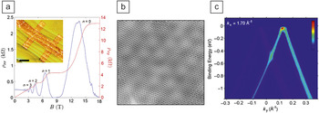
We demonstrated the quantum Hall effect in high mobility (20,000 cm2 V–1 s–1) C-face monolayersReference Wu, Hu, Ruan, Madiomanana, Hankinson, Sprinkle, Berger and de Heer26 (Figure 5a). However, since multilayers have at least one layer that is not at the surface, which is more susceptible to contamination and disorder due to processing, it could be that multilayers are even more important than monolayers, especially for applications (Figure 6). In 2005, we were developing methods to pattern Hall bars on both the Si- and the C-face of graphene, primarily using e-beam lithography methods. We noted that the C-face consistently exhibited higher mobilities than the Si-face, which are found to be in the range of 500–2000 cm2 V–1 s–1.Reference de Heer, Berger, Wu, First, Conrad, Li, Li, Sprinkle, Hass, Sadowski, Potemski and Martinez25 Moreover, we found from transport measurements that the C-face samples always exhibited the signature of graphene, as was clear from the non-trivial Berry’s phase in the Landau levels.Reference de Heer, Berger, Wu, First, Conrad, Li, Li, Sprinkle, Hass, Sadowski, Potemski and Martinez25, Reference Berger, Song, Li, Wu, Brown, Naud, Mayou, Li, Hass, Marchenkov, Conrad, First and de Heer27 We explicitly demonstrated that a multilayer graphene ribbon grown on the C-face had mobilities exceeding 30,000 cm2 V–1 s–1 and showed evidence of quantum confinement.Reference de Heer, Berger, Wu, First, Conrad, Li, Li, Sprinkle, Hass, Sadowski, Potemski and Martinez25, Reference Berger, Song, Li, Wu, Brown, Naud, Mayou, Li, Hass, Marchenkov, Conrad, First and de Heer27
C-face epitaxial graphene. (a) Quantum Hall effect of a graphene monolayer with a mobility of 20,000 cm2 V–1 s–1;Reference Wu, Hu, Ruan, Madiomanana, Hankinson, Sprinkle, Berger and de Heer26 (b) scanning transmission microscopy image of multilayer epitaxial graphene (MEG) showing the characteristic Moiré pattern; (c) angle-resolved photoelectron spectroscopy of MEG showing two intersecting Dirac cones due to two adjacent layers.Reference Miller, Kubista, Rutter, Ruan, de Heer, First and Stroscio32 Due to the electronic decoupling of the layers, the cones do not perturb each other.

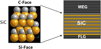
Schematic diagram of graphitized silicon carbide showing the atomic structure (gray atoms are carbon; yellow atoms are silicon). Multilayer epitaxial graphene (MEG) grows on the C-face (with up to 100 decoupled graphene layers), and few layer graphite (FLG) grows on the Si-face (with up to about 10 Bernal stacked graphene layers).

At the same time, our collaborators in Grenoble were measuring the infrared absorption properties of C-face graphene multilayers in magnetic fields.Reference Sadowski, Martinez, Potemski, Berger and de Heer28 They found that the Landau levels dispersed as they would for free graphene layers. This meant that this material is not at all like graphite, but that the layers are essentially decoupled from each other. Moreover, room-temperature mobilities, as determined from Landau level spectroscopy of the material, were found to be extremely large (on the order of 250,000 cm2 V–1 s–1).Reference Orlita, Faugeras, Plochocka, Neugebauer, Martinez, Maude, Barra, Sprinkle, Berger, de Heer and Potemski29 All of these measurements indicated that we had found a new and important graphene-based material, which we named multilayer epitaxial graphene (MEG).
Phil First had demonstrated Moiré patterns due to the interference of two rotated layers of graphene (Figure 5b).Reference Hass, Varchon, Millan-Otoya, Sprinkle, Sharma, de Heer, Berger, First, Magaud and Conrad30, Reference Sprinkle, Siegel, Hu, Hicks, Soukiassian, Tejeda, Taleb-Ibrahimi, Fa¨vre, Bertran, Berger, de Heer, Lanzara and Conrad31 Ed Conrad had performed many crystallographic studies (Figure 5c) of MEG and confirmed the “rotational stacking,” that is the non-Bernal stacking, of the layers.Reference Miller, Kubista, Rutter, Ruan, de Heer, First and Stroscio32 He recognized that the stacking involved specific commensurate graphene structures. Subsequently, the electronic decoupling of the layers was explained theoretically.Reference Hass, Varchon, Millan-Otoya, Sprinkle, Sharma, de Heer, Berger, First, Magaud and Conrad30, Reference Sprinkle, Siegel, Hu, Hicks, Soukiassian, Tejeda, Taleb-Ibrahimi, Fa¨vre, Bertran, Berger, de Heer, Lanzara and Conrad31
It is relevant to note that at that time, many theoretical physicists working on graphene were focused on freestanding monolayers, and they were not interested in dealing with the complications of substrates or multilayers. Many believed that the silicon oxide surface on which exfoliated graphene flakes were deposited did not perturb the electronic structure. However, for metals and SiC, they thought that the substrate essentially perturbed the electronic structure of the graphene, even though experimentally this was known not to be the case.Reference Gall, RutKov and Tontegode10 On the other hand, as explained earlier, exfoliated graphene deposited on oxidized degenerately doped silicon wafers is ideally suited for 2D electron gas studies, because the charge density on the graphene can be continuously varied. This is not so simple in epitaxial graphene.
Various collaborators have since performed many measurements on MEG. Notably, scanning probe experiments performed by Sprinkle et al. at the National Institute of Standards and Technology, using high magnetic fields and low temperatures, demonstrated properties of this material in the quantum Hall regime by essentially imaging the electronic wave functions in the graphene.Reference Miller, Kubista, Rutter, Ruan, de Heer, First and Stroscio32 These experiments also showed the extreme high quality of (at least) the top graphene layer of MEG, which was shown to be continuous over the whole surface.
The carbon layers grown on the Si-face are distinctly graphitic: They are Bernal-stacked, and the layers are electronically coupled. While these thin graphite layers are certainly useful, the relatively low mobilities of the graphene monolayers appear to be problematic for applications and fundamental physics.
Ted Norris of Michigan State University performed ultrafast laser pump-probe measurements to demonstrate the terahertz response of MEG.Reference Sun, Wu, Divin, Li, Berger, de Heer, First and Norris33 These experiments explore the ultrahigh frequency domain, which is the next important frontier in electronics.
MEG is also ideally suited for chemical functionalization and intercalation studies. At GIT, we had first demonstrated that MEG on a SiC chip can be converted into multilayer graphene oxideReference Wu, Sprinkle, Li, Ming, Berger and de Heer34 using standard oxidation processes previously used for graphite. This material is a wide bandgap semiconductor, because the graphitic sp 2 bonds are converted into diamond-like sp 3 bonds. Graphene functionalizaton by this method is crude. Haddon and co-workers have performed much more controlled experiments to affect a related conversion with aryl groups.Reference Bekyarova, Itkis, Ramesh, Berger, Sprinkle, de Heer and Haddon35
These are but a few of the many experiments that are currently in progress on MEG, which may prove to be the ideal material for graphene-based electronics. However, much work remains to be done.
Beyond the extended sheet: Structured graphene growth
Besides fundamental graphene studies, very few applications require extended graphene sheets. Most require patterned structures, and many require extremely fine structures. The predominant paradigm is to produce a large graphene sheet that is subsequently cut to the required shape, typically by using standard microelectronics lithography methods. This method is similar to the way a tailor would produce a garment from a sheet of material.
However, other methods may well be more efficient, where the graphene is grown in its ultimate form, much like a knitted garment is produced. The advantages are clear: this method avoids rough graphene edges resulting from the final plasma etching step. Rough edges degrade transport properties.Reference Sprinkle, Ruan, Hu, Hankinson, Rubio-Roy, Zhang, Wu, Berger and de Heer36 The GIT group developed several approaches along these lines. The most promising of these relies on the graphitization of structured SiC surfaces.Reference Sprinkle, Ruan, Hu, Hankinson, Rubio-Roy, Zhang, Wu, Berger and de Heer36
Our experiments confirmed that various crystal faces of SiC graphitize at different rates.Reference Gall, RutKov and Tontegode10 For example, at a given temperature, the Si-face graphitizes much slower than the C-face. We conjectured that the sidewall of a step etched into the C-face of a SiC crystal would graphitize much more rapidly than the Si-face, so by using correct temperatures and annealing times, the sidewalls would graphitize while the horizontal surfaces would remain ungraphitized.
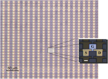
This guess turned out to be correct.Reference Sprinkle, Ruan, Hu, Hankinson, Rubio-Roy, Zhang, Wu, Berger and de Heer36 We recently demonstrated that very narrow graphene ribbons can be produced by graphitizing either natural steps on the surface or steps that had been produced using lithography and etching methods (Figure 7).Reference Sprinkle, Ruan, Hu, Hankinson, Rubio-Roy, Zhang, Wu, Berger and de Heer36 While this route has only begun to be explored, the initial results are quite promising for high mobilities of the graphene ribbons made by this method.
Optical image of a portion of a 10,000 array of transistors produced using sidewall graphitized channels. The inset shows one of the transistors. S, source; D, drain; G, gate. The scale bar in the inset is 10 μm.

Conclusion
This brief overview summarizes the phases of the development of graphene-based electronics at the Georgia Institute of Technology (GIT). The epitaxial graphene on the SiC path to graphene-based electronics, pioneered by the GIT group and developed by its immediate collaborators worldwide, has been adopted by many research groups around the world. Seyller and co-workersReference Emtsev, Bostwick, Horn, Jobst, Kellogg, Ley, McChesney, Ohta, Reshanov, Röhrl, Rotenberg, Schmid, Waldmann, Weber and Seyller37 developed an inert gas annealing process to produce high-quality graphene on the Si-face. Recently, an IBM group produced 100 GHz transistorsReference Lin, Dimitrakopoulos, Jenkins, Farmer, Chiu, Grill and Avouris38 funded by this project using our methods.Reference Kedzierski, Hsu, Healey, Wyatt, Keast, Sprinkle, Berger and de Heer39 A collaborative project in Sweden and England has recently demonstrated that epitaxial graphene Hall bars are ultrahigh precision resistance standards, using the quantum Hall effect at liquid helium temperature.Reference Tzalenchuk, Lara-Avila, Kalaboukhov, Paolillo, Syvajarvi, Yakimova, Kazakova, Janssen, Fal’ko and Kubatkin40
While we are still very far from our ultimate goal of producing integrated epitaxial graphene circuits, there are no obvious show-stopping impediments toward this goal. It is likely that this development will progress slowly, but ultimate success seems likely, and it is a matter of time before the first such devices will be commercially available.
In closing, I would like to address a major misconception that the ultimate goal of graphene-based electronics is to replace silicon. This is not true. It is not likely that silicon will ever be replaced. It has established its role in electronics probably for centuries to come. However, the point is not to replace silicon but to find a successor to it, that is, to develop a material that can outperform silicon where silicon hits the “brick wall” in terms of speed, feature size, or energy consumption. However, for applications where those limitations are not a concern, silicon will continue to be the material of choice, because it is not likely that any form of electronics will be cheaper than silicon in the foreseeable future.
The appropriate analogy is probably with transportation. Goods are carried both by planes and boats. The metal hulled ships of today are essentially identical to the ships built a century ago. Shipbuilding has matured, and there is little innovation left. Sea transport is cheap but slow. Planes, on the other hand, are fast, and the technology is still significantly advancing after the first pioneering flights a century ago. Air travel is fast but expensive. But both modes of transportation coexist harmoniously. So it might eventually be with silicon- and graphene-based electronics. Epitaxial graphene electronics has just made the equivalent of its first 100-foot flight and still has a long way to go before it will be able to make its full impact in electronics.
Acknowledgments
The Georgia Institute of Technology graphene electronics research project was first funded by Intel Corp. in 2003, later by the National Science Foundation in 2004, the Keck foundation in 2008, and the Air Force Office of Scientific Research in 2010.
Walt A. de Heer is a Regents Professor of Physics at the Georgia Institute of Technology. He received a PhD degree in physics from the University of California, Berkeley in 1985, where he continued as a postdoctoral fellow. He has published more than 100 articles, with a total of 17,000 citations. De Heer is a fellow of the American Physical Society and received the IBM Faculty Fellowship Award in 2007 and 2008, and the Sigma Xi Sustained Research Award in 2008. He can be contacted by e-mail at deheer@physics.gatech.edu.