Principal applications for 3D stacked integrated circuits
Advancements in wireless technology have transformed the mobile phone from a simple voice communication device to a handheld personal system with constant connection to the internet. Over the last decade, the modem data rate has increased by a factor of 1001 and is projected to grow by another 10× in the next five years.
In order to support higher performance at lower power levels (as required for battery powered devices), interconnect delays (where long delays will slow down the data exchange between circuits and reduce system performance) and power losses must be reduced—forcing the need for tight packing of components. Tight packaging will reduce the length of the interconnect, thus reducing the delay and parasitic capacitance (lower capacitance will lead to lower power consumption). A very high level of component integration is required, not only to enable compact device form factors desired by the consumer, but also to accommodate aggressive performance requirements. The essential elements within the mobile system that are largely responsible for the speed, efficiency, and power are logic processors and memory. The processor receives and executes every command and performs calculations. The memory stores command instructions and data. A tight integration between the logic processor and memory or logic processor to logic processors will provide high value to the mobile system.
Memory and logic integration
In addition to internet browsing and personal communications, smart phones perform multiple tasks, such as computing, multimedia playback, mapping, and navigation with GPS. To support these broad applications, the performance of the main processor for mobile devices had to be dramatically increased. High performance processors have driven up the quantity of data between the cores and the memory (internal and external), which requires a higher memory storage density.
On-chip memory, such as static random access memory or embedded dynamic random access memory (DRAM), provides high bandwidth and low latency access to the processor but typically has limited density. Since these memories are by definition built using process technology optimized for logic fabrication, implementation of large density memory would be cost-prohibitive. Off-chip memory (DRAM) is fabricated in a dedicated memory process, which can provide high densities (gigabits per die) at relatively low cost; therefore it is used for the main system memory in mobile phones.
Several topologies are implemented to connect a logic processor to external DRAM, including:
• Surface mounting packaged DRAM on the motherboard and connecting to the processor through the printed circuit board (PCB) metal trace (Figure 1a).Reference Carson, Kim and Yoon2
• Stacking the DRAM die on the processor die internally in a single package (internal stacked memory [ISM])Reference Carson, Kim and Yoon2 and connecting memory to a processor through wire bonds and package substrate (Figure 1b).
• Stacking packaged DRAM on top of the processor package (package on package)Reference Carson, Kim and Yoon2 and connecting memory to a processor through ball grid array (BGA) balls, or solder balls, attached to landing pads on the top logic package, through mold vias and package substrate (Figure 1c).
Current memory package to logic chip integration: (a) side-to-side stacking on printed circuit board (PCB); (b) internal stacked memory (ISM); and (c) package on package.Reference Carson, Kim and Yoon2 Note: BGA, ball grid array.

These solutions experience performance limitations because wire bond pads (used in DRAM and ISM packages) and solder bump sizes (solder joints used for packages) cannot be scaled significantly, thereby limiting the number of connections (and data bandwidth = product of pin count and frequency, where the pin count is the number of signal connections) between the dies. Consequently, the typical I/O width (input/output signal counts) of low power double data rate memory is limited to ×32. To achieve higher bandwidths, higher frequency of operation is required—more than 1.066 GHz for each I/O. High drive strength buffers, termination resistors, and other special circuit techniques are required to enable high-frequency I/Os, which adds extra area to the chip, complexity to the package, and hence, cost to the overall component. In addition, since mobile devices run on battery power with limited capacity, it is very important to lower operating power. One key contributor to system power consumption is chip I/O power. With the memory–processor integration solutions described previously, the parasitic load of the interconnect is high.
An alternative approach to scaling memory bandwidth is to increase the number of I/Os rather than the I/O frequency—resulting in a wide I/O memory. Wide I/O (×512) memory has been demonstrated by several memory suppliers.Reference Kim, Oh, Lee, Lee, Hwang, Hwang, Na, Moon, Kim, Park, Ryu, Park, Kang, Kim, Kim, Bang, Cho, Jang, Han, Lee, Choi and Jun3 With a high count of I/Os, the operation frequency of each I/O can be lowered to 200 MHz. Kang et al.Reference Kang, Chung, Heo, Park, Lee, Kim, Ahn, Cha, Ahn, Kwon, Lee, Joo, Kim, Jang, Kim, Choi, Chung, Yoo, Choi, Kim and Jun4 reported that wide I/O memory can lower overall memory active power by up to 50% for a given bandwidth. The challenge with this approach is that a high density of memory to processor interconnections is required.
One alternative is to lay memory and processors side by side in a package and use wafer level fine pitch redistribution metal layer (RDL) and fine pitch microbumps for chip-to-chip interconnects. This integration scheme, illustrated in Figure 2a,5 is referred to as 2.5D integration (side-to-side chip integration) using an interposer.Reference Sunohara, Tokunaga, Kurihara and Higashi5 The chip-to-chip interconnect count is limited by the pitch of the microbumps used to attach the die to the interposer. With this integration scheme, the chip-to-chip interconnect length is typically still relatively long (∼1 mm).
Alternative memory chip-to-logic chip integration: (a) 2.5D interposer and (b) through-Si via (TSV) three-dimensional integration.Reference Sunohara, Tokunaga, Kurihara and Higashi5 Note: PCB, printed circuit board; BGA, ball grid array.
Another alternative is to stack the memory on top of the processor and to connect them using through-Si vias (TSVs). This scheme, referred to as 3D integration (three-dimensional integrated circuit [3D IC]), is illustrated in Figure 2b. The chip-to-chip interconnect count is still limited by the size of the microbumps used to attach die to die, but the length of interconnect between the dies is much shorter. Three-dimensional integration enables vertical connection between chips, which could provide the shortest interconnects and lower the parasitic load. In comparison to wire bonding, the I/O power can be reduced by more than 80%.Reference Gu, Marchal, Facchini, Wang, Suh, Lisk and Nowak6
Logic–logic integration
In addition to memory and logic integration, 3D TSV integration can also enable logic-to-logic die stacking. For the past four decades, Moore’s Law has enabled transistor count doubling roughly every 18 months while maintaining the same cost. However, at process nodes below 14 nm, the Si process reaches critical physical limits, in particular with lithography processing. The fabrication cost is projected to increase significantly due to multiple patterning steps, which have to be employed to achieve the required pitch reduction. In addition, since a single node-to-node scaling factor cannot be applied to all circuits contained in a typical system on a chip (SoC) (e.g., analog circuitsReference Wei, Singh, Bouche, Zaleski, Augur, Senapati, Stephens, Lin, Rashed, Yuan, Kye, Woo, Zeng, Levinson, Wehbi, Hang, Ton-That, Kanagala, Yu, Blackwell, Beece, Gao, Thangaraju, Alapati and Samavedam7 cannot scale as effectively as digital switches), the area and cost benefit traditionally derived from scaling is not there. Hence, there is a potential cost benefit to partitioning a single SoC die into multiple chips, such that only high area scalability circuits (e.g., digital logic) use the most advanced technology nodes, while the less scalable circuits (e.g., analog circuits) leverage the cost and maturity benefits of older technology nodes. For this configuration, the number of connections between chips can be high. Two-and-a-half-dimensional and/or 3D integration, as defined for memory-to-logic integration, can also be leveraged to provide high density connections to re-integrate the partitioned chips into a single system-in-package (multiple chips in one package) as opposed to a SoC.
Three-dimensional chip integration can provide performance, power, and form factor benefits to mobile systems. To enable 3D IC technology, new technology features (e.g., TSVs, microbumps) and new materials are required, as discussed later in the text.
2.5D and 3D integration enabling technologies
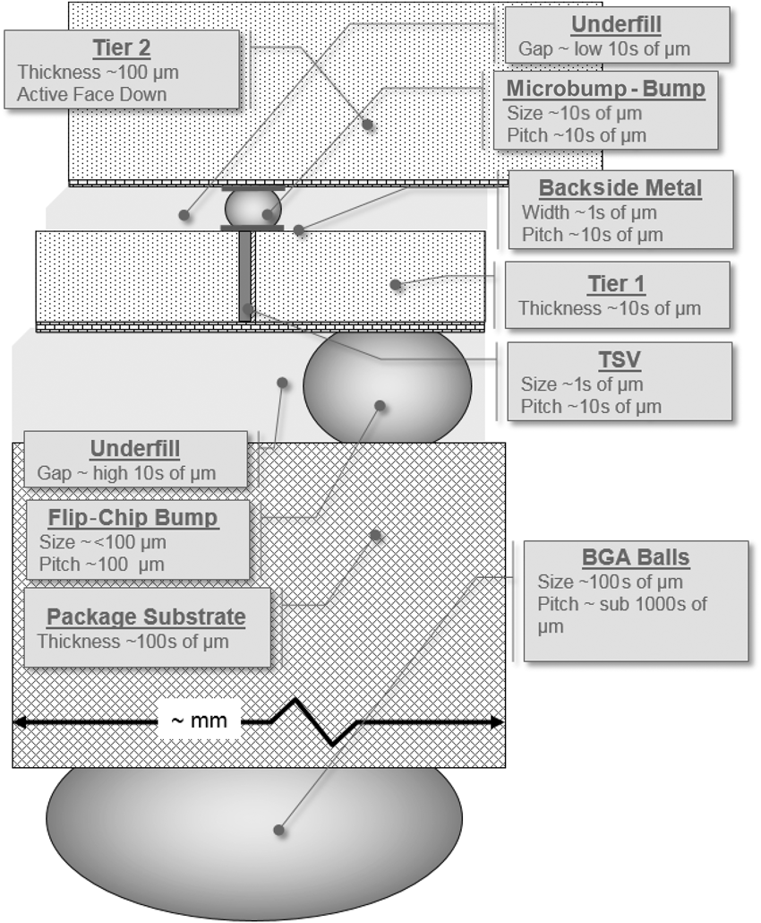
The key enabling technologies for 2.5D and 3D integration include (1) TSVs to make connections through Si; (2) wafer thinning and processing on the backside of the wafer; (3) microbumps or µpads to join the die; (4) flip-chip bumps to connect the die stack to the package substrate; and (5) BGAs to connect PCBs.
These features are illustrated in Figure 3 for a selected packaging technology. Process modules have been developed to fabricate each feature, and multiple integration flowsReference Kim, Vidhya, Henderson, Ray, Gu, Zhao, Radojcic and Nowak8 have been defined to integrate the modules into a complete manufacturing and assembly flow.
Schematic of three-dimensional integrated circuit interconnect and components. Note: TSV, through-silicon via; BGA, ball grid array.Reference Radojcic, Nowak and Nakamoto14

TSV formation
TSV is a vertical interconnect through Si and should provide a good electrical connection with minimum resistance from die to die; typically TSVs are filled with either Cu or W, and the fill material must be selected. It should also provide good electrical isolation from the Si substrate or other TSVs. This is typically achieved by using a liner dielectric composed of SiO2 or SiN, and there is a trade-off in managing the coverage and integrity.
In addition, there is a trade-off involved in selecting the point in the baseline complementary metal oxide semiconductor (CMOS) manufacturing flow where the TSV is inserted. The TSV can be fabricated (1) before transistor formation: “via-first” process; (2) after transistor formation but before metal interconnect: “via-middle” process; and (3) after full device wafer fabrication: “via-last” process. The via-middle and via-last processes are compatible with the use of Cu fill, whereas via-first can only be filled with polysilicon, due to the temperature requirements driven by front-end-of-the line processing. Via-last that lands on the upper layers of interconnect is the easiest to manufacture, but typically takes up the most room.
Finally, there is also a trade-off associated with via diameter and wafer thickness. The TSV etch, liner, and fill processes are all strongly affected by the aspect ratio of the viaReference Dukovic, Ramaswami, Pamarthy, Yalamanchili, Rajagopalan, Sapre, Cao, Ritzdorf, Wang, Eaton, Ding, Hernandez, Naik, Mao, Tseng, Cui, Mori, Fulmer, Sirajuddin, Hua, Xia, Erickson, Beica, Young, Kusler, Kulzer, Oemardani, Dai, Xu, Okazaki, Dotan, Yu, Lazik, Tran and Luo9 (ratio of depth to diameter of the TSV), and current practical process limitations dictate that the aspect ratio must be less than about 10:1. In order to minimize the impact on the Si die area, a small TSV diameter is desired; an application that requires 1000s of vias 10 µm in diameter results in the addition of ∼1 square mm to the die area. On the other hand, handling very thin Si is difficult; a 50-µm-thick wafer is the current practical lower limit for handling wafers without a bonded carrier (physical support). Consequently, the typical current state of the art is a TSV with a diameter of ∼5 µm and a wafer thickness of ∼50 µm.Reference Redolfi, Velenis, Thangaraju, Nolmans, Jaenen, Kostermans, Baier, Van Besien, Dekkers, Witters, Jourdan, Van Ammel, Vandersmissen, Rodet, Philipsen, Radisic, Heylen, Travaly, Swinnen and Beyne10
For the via-middle process, a plasma-enhanced chemical vapor deposition (PECVD) oxide is often used for the TSV liner. However, the PECVD oxide thickness on the bottom of TSV is <50% of that at the top sidewalls. Atmospheric pressure CVD O3/TEOS (tetraethoxysilane) or plasma-enhanced atomic layer deposited SiO2 has provided liners with >80% coverage throughout the TSV. In addition to the film conformity requirement, the liner should provide electrical isolation between TSV and Si substrate under bias. Defective liner material results in leakage currents and/or shorts. Successful tuning of the liner dielectricReference Dukovic, Ramaswami, Pamarthy, Yalamanchili, Rajagopalan, Sapre, Cao, Ritzdorf, Wang, Eaton, Ding, Hernandez, Naik, Mao, Tseng, Cui, Mori, Fulmer, Sirajuddin, Hua, Xia, Erickson, Beica, Young, Kusler, Kulzer, Oemardani, Dai, Xu, Okazaki, Dotan, Yu, Lazik, Tran and Luo9 has been reported, resulting in high yielding, leakage free, via-middle TSVs. For the via-last process, the wafer is thinned before via formation, thereby requiring carrier support. The carrier glue limits the thermal budget for TSV and liner formation to ∼200°C. At this low temperature, a high conformity and low defect liner is not currently available and still needs to be developed.
Cu can diffuse through SiO2 easily, potentially causing problems in the Si itself, so a good barrier is required for Cu-filled TSVs. Physical vapor deposition (PVD) (sputtering) of Ta is used for Cu TSV and has been demonstrated to be an effective barrier against Cu diffusion. However, the PVD coverage of the TaTaN at the TSV bottom is <10% of the top film thickness.Reference Dukovic, Ramaswami, Pamarthy, Yalamanchili, Rajagopalan, Sapre, Cao, Ritzdorf, Wang, Eaton, Ding, Hernandez, Naik, Mao, Tseng, Cui, Mori, Fulmer, Sirajuddin, Hua, Xia, Erickson, Beica, Young, Kusler, Kulzer, Oemardani, Dai, Xu, Okazaki, Dotan, Yu, Lazik, Tran and Luo9 A thick barrier film is required, driving up the processing cost. A low-cost barrier layer process capable of high conformity in a 10:1 TSV is therefore highly desired and needs to be developed.
Great progress has made in the electrical plating of void-free Cu inside a TSV by improving the plating chemistry and process conditions.Reference Chang, Chang, Chen, Kuo, Chien, Liao, Lin, Wei, Lin, Chen, Yang, Teng, Tsai, Tseng, Chen, Hsieh, Chen, Liou, Wu, Hou, Chiou, Jeng and Yu11 Therefore, the actual Cu filling of a TSV is an established and stable process module. However, since the coefficient of thermal expansion (CTE) of Cu is much higher than that of Si, temperature cycling (either during subsequent manufacturing and assembly processing or during system assembly) may result in the plastic deformation of the Cu and/or may distort structures on top of the TSV. Further improvement in the control of the Cu grain structure and impurity levels is required to minimize the impact of this “Cu pumping” phenomenon.
Thinning Si and backside processing
The typical full Si wafer thickness used in a fab is about 760 µm. As mentioned, the TSV depth is only ∼50–100 µm. Therefore, thinning of Si wafers to reveal the bottom of the TSV is an intrinsic requirement for 2.5D and 3D ICs. This necessitates handling thin Si wafers in fab or in shipping to external entities for assembly and/or testing.
Upon completion of the Si fab process, wafers are mounted onto temporary carriers, bonded with glue, and thinned by grinding the wafer on the backside. Often an (optional) incremental chemical mechanical polish step is used to reveal the TSVs and polish off the damage induced by grinding. An insulator is deposited on the backside of the wafer, and a conductor layer—typically RDL Cu—is deposited and patterned to form micropads on the bottom of TSVs and/or (optional) backside interconnect. Note that there is a potential trade-off associated with the use of the backside RDL; its use allows more degrees of freedom in design but adds to the overall process cost and complexity. After µPad formation, the wafer is demounted from the carrier and processed further for stacking and assembly.
Since the wafer undergoes processing on the carrier, the glue must tolerate the backside processing, including high temperatures, exposure to chemicals, plasma, and mechanical stress from grinding. This dictates the need for glues that provide strong adhesion of wafers to carriers; however, the thinned—and fragile—wafer must also be easily demounted from the carrier, requiring fairly weak glue adhesion. These contradictory requirements have to be met.
After the wafer is mounted on the carrier, thermal or ultraviolet (UV) curing of the glue is employed to provide the required adhesion between the wafer and the carrier. To demount the wafer, the glue (typically a thermoplastic) can be softened at high temperatures, and then the wafer can be separated from the carrier. In this case, a high temperature is required for demount, which is not desired for some devices. Alternative UV laser ablation through the glass carrier can separate the carrier from the glue at room temperature; the glue can be removed either by chemical stripping or mechanical peeling. Thermoplastic and thermal setting materials have been demonstrated for successful carrier mounting and demounting.Reference Tsai, Chang, Chien, Lau, Fu, Chiang, Kuo, Chen, Lo and Kao12 However, these demonstrations have been mostly conducted in low volume applications, and additional carrier glue material innovations are needed for reliable and low cost temporary bond-debond processing in high volume manufacturing. In addition, thin wafers (∼50–100 µm) are susceptible to breakage/damage during shipping. Innovative materials and solutions that can provide support for thin wafer shipping without introducing new defects or contaminants are highly desired.
Microbump joints between chips
Typically, the flip-chip solder bump pitch used to connect die to package substrate is of the order of 100 µm. In order to achieve high density of interconnects between dies, the microbump used to connect one die to another die for 3D stacking is around 40 µm. Typical microbumps currently used in the industry are composed of a Cu post, an optional solder diffusion barrier such as Ni film, and a layer of solder for the actual joint.Reference Liu, Li, Kim, Gu, Parkinson, Blair and Tu13 To ensure a good connection yield for all I/Os, the solder layer thickness must exceed the microbump height variation and must accommodate worst case die warpage. If the die warpage and coplanarity are good, then microbump joints can be formed by mass reflow, followed by capillary underfill between chips to enhance the joint strength. If the coplanarity and warpage are high, then an external force must be applied during bonding to flatten the thin die at a high temperature (i.e., thermal compression bonding must be used). If the gap between the dies is small, then the underfill can be pre-applied prior to stacking by the use of a suitable non-conducting paste or film. Fillers that are usually incorporated in the underfill to improve its modulus can be trapped between the die or in the solder joint, as shown in Figure 4.Reference Liu, Li, Kim, Gu, Parkinson, Blair and Tu13 With the microbump height and diameter reduced down to ∼20 µm, the susceptibility to interaction with filler defects is enhanced. Optimization of the underfill filler shape, size, distribution, and rheology is required to minimize filler traps for the stacking process.
Cross-section of a typical microbump: (a) arrays and (b) high magnification image of one microbump (fillers are within the underfill between microbumps and some are trapped within the solder).Reference Liu, Li, Kim, Gu, Parkinson, Blair and Tu13
Package bump and assembly
Package components are usually attached to the PCB using a surface mounting process and BGA solder ball attachment. Typical pad pitch on the PCB is of the order of 400–1000 µm, much higher than the flip-chip solder bump pitch (∼100 µm). A package laminate substrate is used to fan out the ∼100 µm flip-chip bump pitch to the ∼400 µm BGA ball pitch and provide suitable redistribution of power, ground rails, and other chip utilities. A 3D IC stack must also use a laminate substrate (or some other way of providing the fan-out). The sequence of attaching the (at least) three elements (two dies and one substrate) in the stack needs to be defined and optimized. Several flows can be used to complete the stacks:Reference Kim, Vidhya, Henderson, Ray, Gu, Zhao, Radojcic and Nowak8
• Attach the logic die to the laminate substrate first using flip-chip, and then stack the second die (or cube) on the back of the logic die using the microbump. This is called die-to-substrate (D2S) flow.
• Stack two (or more) dies first using a microbump attachment, and then attach the die stack to the laminate substrate using flip-chip bumps. This is called die-to-die (D2D) flow.
• Stack the second die to the backside of the first die wafer using a microbump attachment, singulate the wafer into individual die stacks, and then attach the stack to the laminate substrate using a flip-chip attachment. This is called die-to-wafer (D2W) flow.
The selection of the assembly flow is a trade-off, which impacts the supply chain and sourcing model used and drives process cost, margin, and yield. The key determining factor of flow choice is that warpage of parts during joining should be lower than the solder height. For example, if die 1 and the substrate stack (D2S) warpage (including assistance from the compression bond force) is higher than the microbump solder height, then the second die will not be able to join to the first die for all microbumps (i.e., D2S flow should not be used). Similarly, if D2D stack warpage is higher than the flip-chip bump solder height, then D2D flow should not be used.
The mechanical properties of built-up films and materials within the same package determine warpage. Tuning the properties of the materials used is essential for successful 2.5D and 3D IC assembly. In the example of D2W flow, the second die warpage should be reduced by optimizing the back end of line (BEOL) built-up layer stress such that there is a high yield of successful microbump joints between the second die to the first die. If molding is used post D2W attachment, the molding material should be adjusted such that D2W cube warpage is low. In addition, there is CTE mismatch among the laminate substrate core, built-up layers and Cu, and Si. We need to reduce the substrate CTE and balance the built-up layers between each side of the core, such that the laminate substrate warpage is low enough during D2W cube attachment to the substrate.
An underfill to improve the adhesion between the die and the laminate substrate is critical. Since capillary force is used to pull the underfill material across the gap, material viscosity needs to be tuned such that it can fill the gap without voiding and minimize the overflow outside the chip area.
Finally, 2.5D and 3D stacked ICs enable high densities and relatively short interconnects between dies, enabling the use of minimum size drivers (I/O switch driver that switches the signal from low to high voltage or vice versa) and I/Os, thereby allowing for significant power (and area) savings. The value proposition of small I/Os can be eroded if a large protection circuit for managing charging and electrostatic discharge (ESD) phenomena is required. Manufacturing and handling processes have to be optimized to minimize the charging/ESD events, which in turn would allow designs with small, or no, protection circuits. Therefore, materials that can help eliminate ESD charging during manufacturing and shipping are required
2.5D and 3D integration technology characteristics
Electrical performance
As mentioned previously, one of the value propositions associated with 2.5D and 3D integration technologies is the ability to reduce power by leveraging very small I/Os driving minimum load sizes. I/O power could further be reduced by optimizing the TSV oxide liner and resorting to a low k value liner (k = dielectric constant), while still maintaining very high conformity to high aspect ratio TSV features. New materials and process technologies are required to develop and deploy these characteristics.
In addition to enabling the I/O interconnects, TSVs are also used to provide power and ground connections for the die higher up in the stack. High TSV and/or microbump impedance (R, resistance; L, inductance; C, capacitance) would result in supply voltage droop with an adverse impact on chip performance. Therefore, very low TSV/microbump resistance, including the interface resistance, is required. Hence, optimal metal conductivity, contact interface, and interface cleaning chemistry are desired.
Stress management
CTE mismatch between TSV Cu (∼16 ppm/C) and surrounding Si (∼3 ppm/C), results in a complex stress profile that depends on the thermal profile and history. Typically, Cu fill of via-middle TSV tends to restructure during the BEOL and assembly cycling and is at equilibrium at around 200°C. This means that at room temperature, Cu is pulling on Si, resulting in a radial tensile stress around the TSV. These complex stress-strain relationships can result in Cu extrusion during the manufacturing process (TSV pop up) or during normal field operation (Cu pumping), leading to yield and reliability failures. In addition, mechanical stress affects the Si band structure, impacting carrier mobility and ultimately device performance.Reference Radojcic, Nowak and Nakamoto14 For example, a compressive stress of the order of ∼100 MPa or more along the channel length increases hole mobility, resulting in a higher performing PMOS, which can impact the performance of a device close to the TSV. Therefore, the manufacturing process has to be optimized to manage the mechanical stresses. In addition, typically, keep out zones are defined around TSVs to prevent placement of active devices in the region where their performance can be affected.
As well as Cu-filled TSVs, the interaction of various properties (Young’s modulus, glass transition temperature) of the materials used in stacking and packaging, along with the process conditions used in assembly, play a significant role in the distribution of mechanical stress in finished 2.5D or 3D IC devices. Figure 5 illustrates the impact of microbumps on device mobility for a particular layout configuration used in a 3D stack,Reference Nakamoto, Radojcic, Zhao, Dasarapu, Karmarkar and Xu15 resulting in variability of device performance and adversely affecting the parametric yield. The stresses induced by the assembly process and packaging materials are not unique to 3D ICs (versus TSV stress, which is unique to 2.5D and 3D integration), and similar effects are observed in standard ICs that use thin Si dies.
Simulation of microbump impact to tier 1 Si mobility impact for an example three-dimensional integrated circuit: (a) schematic of the simulation and (b) carrier (electron or hole) mobility change as a function of distance away from microbump.Reference Nakamoto, Radojcic, Zhao, Dasarapu, Karmarkar and Xu15
Consequently, holistic optimization of material properties and process technologies is extremely important to manage and reduce stress effects. Further material development is required to enable technology evolution to thinner dies and smaller TSVs.
Thermal management
Heat generated in a given component, as well as in adjacent components in a mobile system (the chip set, antenna and radio frequency subsystem, memory, display), raises the transistor junction temperature, which impacts carrier mobility and changes device performance. Additionally, high temperature increases transistor leakage currents, which increase the overall power consumption and heat up the device further. Even though the total power consumption of mobile devices is low relative to desktop computers, the small form factor limits the thermal management options for mobile devices. The requirement for a thin body (z-dimension) makes fan-based solutions difficult, and the small body size (x-y-dimensions) limits the total surface area available for passive thermal dissipation. With increased power demands in smartphones, thermal management becomes the critical and intrinsic limit.
By definition, a key value proposition of 2.5D and 3D integration technologies is a compact design, which allows for tight electrical interconnects between dies. However, this compact design also results in higher net power densities and potentially worse thermal challenges. For the same power consumption, the small size of 2.5D and 3D ICs will increase the peak temperature. Since the heat within the die is usually generated in a few local areas, these will generate local hot spots, especially in situations where heat dissipation is limited—as is the case with mobile devices. Thin die and stack thicknesses further reduce local lateral heat conductivity in comparison to a thick stack, thereby exacerbating the local heat flow management challenges. Even though Si and metals have high thermal conductivity, other materials such as underfills and mold have lower thermal conductivity. Therefore, 3D ICs have especially acute thermal challenges in mobile applications. Appropriate thermal management solutions are necessary. Tuning the thermal conductivity of the materials used in the stack could provide relief from these thermal challenges.Reference Oprins, Cherman, Vandevelde, Van der Plas, Marchal and Beyne16
Reliability
Although customers update their phones more frequently than computers, the reliability of all devices is critical. The new processes, structures, and materials used for 2.5D and 3D ICs, worsened by thermal management limitations resulting in higher operating temperatures, can all precipitate incremental reliability risks. Phenomena such as Cu pumping associated with Cu-filled TSVs can precipitate new failure mechanisms. Even though the reliability solutions applicable to the flip-chip bumps and Cu pillars should apply to microbumps, the reduced diameter increases the current density and the potential adverse effect of trapped contaminants, thereby potentially exacerbating the risk of electromigration. The reduction of the solder layer thickness associated with the microbump joints results in more complete conversion of the solder into intermetallic compound (IMC) alloys during the normal thermal cycles experienced during the assembly processes. The IMC composition may change during device operation, potentially resulting in void formation in the IMC layer. Furthermore, the mechanical property mismatch between the materials (underfill, mold, substrate cores, built-up films, Cu, Si) used to build the 3D IC can generate mechanical stress at the interfaces, such that thermal cycling during operation may result in interface delamination. Finally, mobile devices are handheld, and as such are exposed to mechanical shock. Since 3D ICs have more interfacial area than traditional ICs, strong interface adhesion between layers is especially necessary.
Optimization of the process flows, structures, and materials used addresses the TSV reliability risks, and good results for TSV-based 3D ICs have been reported.Reference West, Choi and Vartuli17 Optimization of solder joint metallurgy is also required, especially if the microbump joints are scaled to dimensions comparable to the IMC grain size (ranging from sub-µm to few-µm). Holistic tuning of all material properties is necessary to minimize the residual stress build up. Managing these requirements may be contradictory, and trade-offs and optimization are required. For example, reducing stress between Si and the underfill layer and using low CTE and low modulus underfill material are desired, but utilizing a low CTE material may require high filler content, leading to increased contamination issues. Thus, material innovation and optimization of surface chemistries are vital in order to address these potential reliability challenges.
Summary
In the past few years, great progress has been made with TSV-based 2.5D and 3D ICs. For example, a four-die-wide I/O memory cube stacked on top of a 28 nm CMOS logic die, illustrated in Figure 6, has been successfully demonstrated.Reference Kim, Vidhya, Henderson, Ray, Gu, Zhao, Radojcic and Nowak8 However, most of the 2.5D and 3D IC implementations discussed in the literature have been built either as demonstrator prototypes or in relatively limited volumes. To enable 3D IC for the high volume manufacture of mobile applications, there are still many opportunities for material innovations to improve performance and reliability, and, more importantly, to simplify the process and lower system cost, as summarized in Table I.
Three-dimensional integrated circuit stack wide input/output (I/O) memory cube on the back of a logic chip: (a) schematic and (b) cross-sectional image. Note: BGA, ball grid array; TSV, through-silicon via; MPGA, I/O micropillar grid array package.
Three-dimensional integrated circuit (3D IC) material improvement opportunities.
Note: TSV, through-silicon via; k, dielectric constant; EM, electromigration; HVM, high volume manufacture; CTE, coefficient of thermal expansion; BGA, ball grid array.
Acknowledgments
The author would like to thank D.W. Kim, R. Radojcic, B. Henderson, M. Nakamoto, U. Ray, and M. Nowak for discussions of 3D IC development challenges. In addition, the author would like to thank King-Ning Tu for discussions of microbump joint metallurgy.