Introduction
The modern advancement of wireless communication has induced contamination of the environment due to electromagnetic interference (EMI). Out of all the known sources of pollution, electromagnetic (EM) pollution has turned the table and increased fourfold. Currently, the pollution due to EM radiation is one of the largest growing factors in degrading the environment. It not only harms human beings, but it is extremely harmful to animals and their entire biological life. To reduce the harmful effects of EM radiation, several important innovations have been successful in suppressing them. Out of these, the use of metamaterials (MMs) has shown positive results in the suppression of EMI. EM MMs are artificially engineered materials that make use of sub-wavelength dielectric or metallic elements, giving rise to exotic properties which are not available in nature [Reference Munk1]. These properties arise due to the structural features rather than material constituents. The structural parameters such as size, shape, and geometry can be adjusted to obtain tunable permittivity and permeability values of the MM structure. These MMs have exhibited quite unusual properties such as left-handed behavior, near-zero permittivity, permeability, double-zero behavior, negative refractive index, etc. [Reference Caloz and Itoh2]. These MMs have shown applications in various multiple disciplines such as EMs, optoelectronics, biomedical devices, ranging from low microwave to visible frequency [Reference Landy, Sajuyigbe, Mock, Smith and Padilla3]. The most popular applications of MMs are that of the development and design of EM absorbers. The properties of MMs can be achieved by suitably designing these absorbers, along with perfect absorption, which is our main aim in suppressing EMI.
Microwave absorber (MA) materials are used to reduce EMI and enhance the isolation among devices. MAs are used to reduce the amount of energy present in the microwave signal. The structure of an MA consists of unit cells arranged periodically. The top layer consists of a conducting layer with the bottom layer used as the ground plane and a dielectric layer in between both the layers. The principle of absorption primarily deals with impedance matching using a dielectric layer. Its impedance Z in must match with 377 Ω, i.e. the impedance at free space. This would result in zero reflection coefficient, thus maximum absorption occurs. Thus, the incident wave penetrates the dielectric layer. In MAs, since the top layer is conducting, its surface charges get energized with the electric field, which results in a magnetic response, thus causing absorption at the resonant frequency. The current which is generated is circulating as well as parallel, which further induces magnetic and electric responses, respectively. The strong coupling between the electric and magnetic responses gives rise to this current. They couple with the EM wave and very strong electric and magnetic resonances appear at this resonant frequency, thus providing very good EM wave absorption under the matching condition [Reference Watts, Liu and Padilla4]. Mostly in the practical implementations, the cause of EMI is unspecified, as in it may occur due to several sources, at different frequencies, and of unknown polarization. Achieving perfect absorption, at a very high frequency, often suffers from one or more properties being forfeited. Attaining high bandwidth, with thickness in nanometers and absorption rate of above 90% is difficult, but has been developed to some extent in the recent past. The absorbers which operate in the frequency range of 30–300 GHz are known as millimeter-wave absorbers. In the past, research study has been carried out to design absorbers with suitable materials and structural features, which could help in obtaining large absorptivity. As the research demand grows in this field, there is a quest for the search of novel materials and designs.
The utilization of polymeric composites and ceramics for the designing of absorbers has been a very important area of research in this field. Traditionally, these are composed of magnetic loss materials, such as magnetic metals [Reference Liu, Xu, Xia, Che, Chen, Cao and He5, Reference Lv, Ji, Wang, Shang, Zhang and Du6], ferrites [Reference Wang, Wang, Zhu, Yang, Kong and Liu7, Reference Ji, Cao, Chen, Zhai and Bai8], dielectric loss materials that are composed of materials containing carbon, either carbon fibers [Reference Shah, Wang, Huang, Zhang, Wang, Zhou, Duan, Dong and Zhang9], carbon nanotubes (CNTs) [Reference Makarova, Geydt, Zakharchuk, Lahderanta, Komlev, Zyrianova, Kanygin, Sedelnikova, Suslyaev, Bulusheva and Okotrub10, Reference Nam, Lee and Jang11], or silica carbide fibers [Reference Zhang, Zhang and Zhang12], and conducting polymers [Reference Tian, Du, Xu, Qiang, Wang, Ding, Xue, Ma, Zhao and Han13]. Out of all the above carbonaceous materials, a CNT has been a widely used material due to its extensive properties and high conductivity [Reference Makarova, Geydt, Zakharchuk, Lahderanta, Komlev, Zyrianova, Kanygin, Sedelnikova, Suslyaev, Bulusheva and Okotrub10–Reference Gnidakouong, Kim, Park, Park, Jeong, Jung, Ahn, Han and Park15]. CNTs usually have weak microwave absorption property, so it is combined with other lossy materials to achieve the desired absorptivity [Reference Meng, Wang, Huang, Guo, Wang, Hui and Zhou16]. For example, as in the case of ZnO@CNT [Reference Lu, Cao, Shi, Fang, Yang, Hou, Jin, Wang, Yuan and Cao17], CdS–MWCNTs [Reference Lu, Wang, Cao, Yuan and Cao18], CNT@Fe3O4 [Reference Lu, Cao, Chen, Cao, Liu, Shi, Zhang, Wang and Yuan19], and γ-FeNi/CNT [Reference Yang, Liu, Hui and Chipara20]. The two-dimensional (2D), sp2-hybridized carbon atoms, called graphene, have also shown exceptionally good electrical, thermal, and mechanical properties and are a perfect candidate for microwave absorption. It is capable of dissipation and absorption of EM waves by transforming them into thermal energy [Reference Shahzad, Yu, Kumar, Lee, Kim, Hong and Koo21]. In this paper, we will discuss various recently developed millimeter-wave absorbers based on structural features, followed by those using polymeric composites.
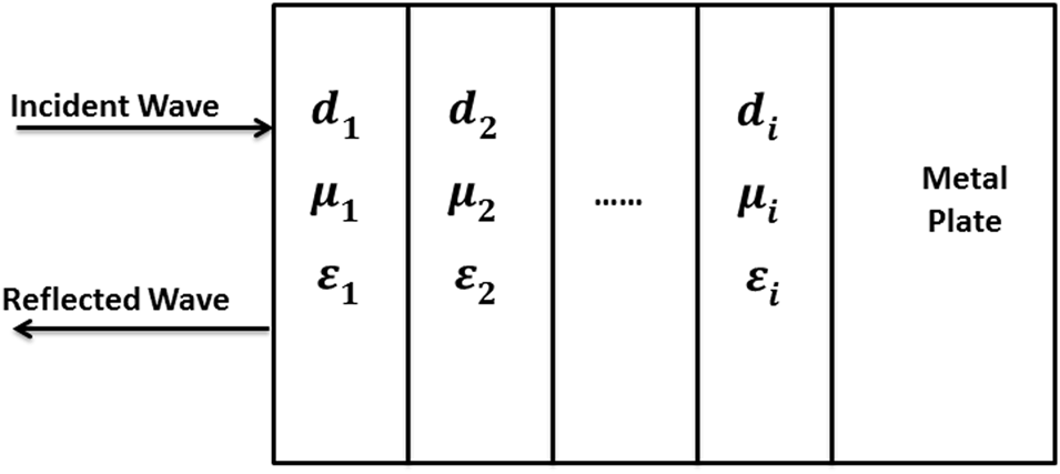
A typical MA looks like as shown in Fig. 1. It consists of i-layers of dissimilar materials, supported by a perfect electric conductor.
Schematic representation of a typical i-layer MA with thickness, permittivity, and permeability, backed by a metal plate.

The two main methods for the characterization of EM materials are non-resonant and resonant methods. The non-resonant method of analysis is mainly focused since it determines the response of electric and magnetic behaviors over a large span of frequencies. Here, the properties of materials are calculated by their wave velocities and impedances in the material medium. The EM parameters of the material are calculated by reflection and/or transmission through the boundary between the free space and material. Coaxial lines, dielectric waveguides, hollow metallic waveguides, planar transmission lines, and free space are used as a medium to carry EM waves to the material.
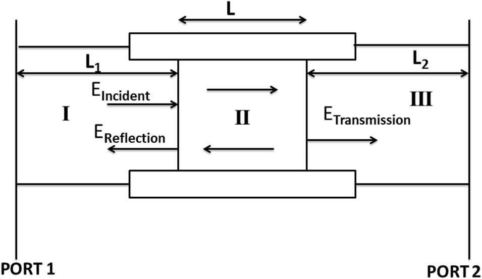
For the reflection method, a single-scattering parameter, S 11 is analyzed, where the signal is transmitted and received through the incident port, or port 1. The permittivity and permeability can be deduced, which are quantified in terms of the scattering parameters. For the transmission or reflection method, two-port systems are used, where the signal incident can be split into the reflected and transmitted waves. This can be modified analytically into a 2 × 2 matrix. The schematic sketch of a two-port system for the analysis of the transmission/reflection method is shown in Fig. 2. Here, the S-parameters are calculated from Maxwell's equations applied with the boundary conditions for the selected material. The material to be studied is positioned into a transmission line. The S-parameter equations are used to calculate the electric field at the interface. The scattering equations consist of variables relating to the permeability, permittivity of the material inserted, length, and the position of reference planes of the sample.
Schematic representation of a measurement setup for transmission/reflection method.

The primary requirements of an absorber are as follows: (1) it should be able to minimize the reflection at the front surface, (2) impedance matching at the free space to absorber interface must be achieved, (3) the absorber must have large values of dielectric and magnetic losses for EM waves to penetrate, and (4) it does not require an external magnetic field [Reference Pitman, Lindley, Simkin and Cooper22]. An absorber with minimal thickness, more particularly in the nanometers range, with high bandwidth and good absorption, are the requirements of 5G technology.
In this paper, we discuss various millimeter-wave broadband absorbers based on structural features and polymeric composites. The design-based challenges are also discussed with various techniques to overcome the same. A comparative analysis of absorptivity for various absorbers is carried out, along with their prospects and applications.
Motivation and outline
In the pursuit of technological advances in the field of communications, we are constantly on the lookout for research interests in the field of EM theory as well as its application in multi-disciplinary sectors. The use of polymers in the microwave industry has drawn attention due to its large design flexibility, low cost, ease of fabrication, and ample tunability of the dopant concentration. By controlling the structural parameters as well as the concentration of dopants in polymer composites, the absorption behavior could be enhanced according to the required application. The filler particles in the polymeric composite give rise to polarization phenomena and therefore provide an understanding of the dependence of frequency on the effective permittivity of the material. In what follows, the different types of structures and polymeric composites to optimize the performance of these millimeter-wave absorbers have been reviewed. To our knowledge, no review has been made in the field of millimeter-wave absorbers based on structure and polymeric composites to date. Although several absorbers have been developed, there are always new objectives to achieve while designing the same, for various applications. Despite the advancement, there are several challenges faced by researchers while developing the same. Some of these challenges are recognized and discussed in this paper. The remaining paper is organized as follows: in Section “Background theory,” we have reviewed the background history of EM wave absorbers, followed by design challenges and techniques to overcome the same in Section “Design challenges.” Section “Recently developed millimeter-wave absorbers” discusses the recent progress in the development of millimeter-wave absorbers. It is divided into two parts: one, discussing the millimeter-wave absorbers based on designing and simulating using frequency simulators; second, absorbers developed by polymeric synthesis. This section has been divided into single- and multi-layered absorbers sub-sections for the ease of reading. Comparative tables for the geometrically designed absorbers as well as those synthesized using polymers have been provided. Section “Conclusion” discusses the prospects, applications, and is finally concluded.
Background theory
The demonstration of the very first MA was made possible by Landy et al. [Reference Landy, Sajuyigbe, Mock, Smith and Padilla3]. This gave rise to a new research interest in the field of microwaves and the absorption theory obtained new domains from microwave to higher bands. The easy realization of a design onto a structure with a suitably good absorption has made it the center of attraction for engineers. In most cases, the origin or the cause of EMI is not certain and may occur in a wide range of frequencies with any polarization, occurring from any direction. Absorbers must be ultrathin and polarization-insensitive, thus achieving a suitably perfect absorption. Despite the requirements, it is difficult to achieve all of them simultaneously. In the recent past, technologies have made it possible to implement flexible and tunable resonators. The composite structures are also useful in acquiring broadband resonance which is not possessed by ordinary mediums [Reference Spada and Vegni23]. Geometrically, absorbers are categorized as resonant and gradient impedance absorbers. Graded absorbers are also called impedance-matching absorbers. In the graded absorbers, the EM waves experience reflection occurring at the air–absorber interface. This reflection is proportional to the magnitude of the impedance of radiation and transmitted medium. Three types of graded absorbers have been prepared in the past, namely pyramidal, tapered, and matching layer absorbers [Reference Seng, Wee, Rahim, AbdulMalek, You, Liyana and Ezanuddin24].
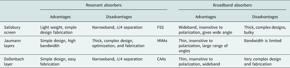
One of the earliest studies in MAs is that of a Salisbury screen absorber [Reference Fante and McCormack25]. It has a thin screen separated by a metallic backing with a dielectric placed at a quarter wavelength from the screen. This is because, in the transmission line theory, whenever a load is kept at a quarter wavelength distance from the metal plate, it forms an open circuit at the resistive sheet, resulting in impedance matching due to zero value of reflection. However, the Salisbury screen suffers from bulkiness and narrow absorption bandwidth. To achieve broadband absorption, Jaumann absorbers were proposed, consisting of multiple resistive sheets and dielectrics. However, the thickness is large. A combination of quarter wavelength thick lossy dielectric material having a metallic ground plane is called a Dallenbach absorber. Multiple stacking of layers is required to achieve broadband behavior. Due to the multiple stacking of layers, the thickness is compromised in this case. One type of broadband absorbers uses a frequency selective surface (FSS). It consists of periodic arrangements of conducting patterns onto a dielectric substrate. These absorbers produce exceptional absorption properties and are substantially light weight. Circuit analog absorbers (CAAs) are made of sheets comprising resistive as well as reactive components. They are realized by using a periodic lossy material as the top layer.
It can be thought of as, at the resonant frequency, the gap between the surface and the bottom layer is a quarter-wavelength. At this point, an RLC equivalent circuit of an absorber experiences resonance. Just like a Jaumann absorber, which consists of multiple resistive sheets, a CAA can be prepared from multiple circuit analog sheets too. It provides large bandwidth but the design and fabrication are quite complex in this case.
Metamaterial absorbers (MMAs) are engineered materials and known for their electric permittivity and magnetic permeability. They are not dependent on any particular property of materials; rather they obtain their novel properties from their geometry or design. By scaling the design parameters, the operating frequency range can be changed [Reference Watts, Liu and Padilla4]. The detailed study of the absorbers in the millimeter-wave frequency range is performed in Section “Recently developed millimeter-wave absorbers.”
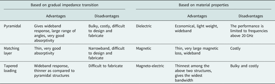
For an absorber prepared from dielectric materials, it is observed that the thickness of the absorber coating is larger as compared to an absorber prepared from a magnetic material. This is because, in pure dielectrics, both parts of the permittivity are very less as compared to that in a magnetic material, which has larger real values of permittivity and permeability. There are no magnetic properties in a dielectric. For hybrid absorbers, the performance is very efficient with less thickness, as it combines the benefits of dielectric and magnetic materials, providing large loss values. Thus, these absorbers are categorized based on geometrical features, materials, and impedance transition. It is demonstrated in Tables 1 and 2.
EM absorbers based on structural features

Absorbers based on gradual impedance transition and material properties

Design challenges
Bandwidth–thickness
The fascinating properties of MMs have made it easy to increase the absorptivity of an EM absorber. However, the electric and magnetic resonance occurring within the structure could limit the absorption bandwidth. The perfect absorption could be achieved for a thin absorber when the operating bandwidth is not much wide. However, when a large absorption bandwidth is required with minimal thickness, the development of such absorbers becomes difficult. For example, an eight-resistive Jaumann absorber was designed and above 80% absorptivity was found from 2.95 to 35.2 GHz, but the thickness was much larger, 31.4 mm [Reference Kazemzadeh26]. For a perfect absorption, it is important to keep a check on the optimal thickness of the absorber as well. The bandwidth and thickness always differ from each other. In simple words, it is difficult to obtain large bandwidth with a very small thickness of the absorber. Therefore, the bandwidth–thickness relationship must be optimized to attain perfect absorption.
Using highly absorbent materials [Reference Lu, Wang, Cao, Yuan and Cao18], including highly lossy materials [Reference Kubo, Ido and Yokoyama27], integrating different resonant units either in the horizontal or vertical direction [Reference Batrakov, Kuzhir, Maksimenko, Paddubskaya, Voronovich, Lambin, Kaplas and Svirko28], utilizing lumped circuits [Reference Zhi Cheng, Wang, Nie, Zhou Gong, Xiong and Wang29], use of magnetic substrates [Reference Zou, Yao, Wei, Gong, Fu, Wang, Jiang, Liao, Yin, Huang and Chen14], anti-reflection coating [Reference Sun, Liu, Dong and Zhou30], based on water [Reference Rotshild, Azoulay, Ochana, Shulzinger and Abramovich31], resistive films [Reference Li and Lv32], use of transparent spacers such as indium tin oxide (ITO) [Reference Yin, Lu, Gao, Yang, Lai, Li and Deng33–Reference Takizawa and Hashimoto37], FSSs [Reference Narayan, Latha and Jha38–Reference Anwar, Mao and Ning40], polymeric nanocomposites [Reference Lozitsky, Vovchenko, Matzui, Oliynyk and Zagorodnii41–Reference Gui, Wang, Wei, Lü, Shu, Jia, Wang, Zhu and Wu46], etc. are some of the techniques to overcome this challenge.
Multi-layering is one of the most efficient approaches to obtain large working bandwidth, by the combination of multiple-resonant elements with varying resonant frequencies, inside a single multi-layered unit cell [38--47--49]. Within this multi-layered structure, each layer adds to the losses, thereby enhancing the absorption with large bandwidth and reduced overall thickness. It requires careful selection of the design parameters to achieve perfect absorption while maintaining the required criteria. The fabrication process in such structures is usually complex due to the limited space in a single unit cell. Nevertheless, multi-layering provides enhanced absorption by combining the resonance of each layer in the structure.
Water, on the other hand, is less electrically conductive with good absorption properties.
In the case of resistive thin films or sheets such as ITO, parallel and anti-parallel current flow takes place that induces electric and magnetic fields. They couple with the incoming waves and causes strong absorption at the resonant frequency.
Polarization and incidence angles
For effective microwave absorption, despite the wide bandwidth and low thickness, it is also required for an absorber to be insensitive to the orientation and polarization of EM radiation. There have been several cases in the past, where absorbers are sensitive to the orientation and polarization of the radiation. Such problems have been tried to resolve to achieve the perfect absorption. It has been reported earlier that on increasing the working bandwidth and incidence angles, it was difficult to control the geometry of the structure as it had to suffer from bulkiness and complexity. As the incidence angle increases, the magnetic couplings among the layers of the absorbers become weak, due to which the magnetic resonance reduces, and hence the absorption performance is affected.
The EM radiation can be incident on the absorber with any angle and orientation, thus it is important to develop absorbers that would be insensitive to these factors to achieve good absorption. The relations of absorption characteristics with that of polarizations are directly dependent on the impedance matching of the absorber with that of free space. For 100% absorption, the effective permittivity and permeability are equal in magnitude. In the transverse electric (TE) polarization, it is linked with the electric field of the incident EM waves. When the electric field is parallel to the structure of the absorber, electric resonance occurs. The magnetic resonance decreases as the incidence angle increases, thus resulting in a reduced magnetic field component into the substrate material. Due to this imbalance, there is a mismatch of impedance between the free space and absorber. Similarly, in the case of transverse magnetic (TM) polarization, it is linked with the magnetic field of the incident EM waves. The magnetic resonance occurs when the magnetic field is parallel to the structure of the absorber. Here, the electric resonance reduces on increasing the incidence angle, thus resulting in a mismatch of the impedance between the absorber and free space. This gives us an insight that structure could not be insensitive to TE or TM polarization at all incidence angles.
Recently developed millimeter-wave absorbers
Based on structural features
Single-layered absorbers
One of the important methods of increasing the bandwidth of an absorber is by using FSSs with highly absorbing materials [Reference Anwar, Mao and Ning40]. In the past, FSS-based absorbers have shown to be a potential method for good absorption. Despite having good absorptivity, these structures are bulky and fragile. Thickness and bandwidth differences in FSS-based absorbers are the main challenges.
A single-layered FSS absorber was designed by Sakran et al. [Reference Sakran, Neve-Oz, Ron, Golosovsky, Davidov and Frenkel39] using metallic nichrome circle on a 0.5 mm thick polymethyl-methacrylate (PMMA) substrate. Also, another absorber was prepared from a nichrome circular ring of 0.25 mm thick on an alumina substrate for the W-band, achieving maximum absorptivity at 95 GHz. This was designed for the application of a micro-bolometer array. Here, it was observed that although the ring array had a lower surface coverage than that of the circular one, it still showed better absorption efficiency. However, the circular array gave a broad bandwidth, due to the higher permittivity of the alumina substrate. Jaumann absorbers are broad bandwidth absorbers [Reference Chambers and Tennant50, Reference Du Toit51]. But, they suffer from the issue of thickness as compared to Salisbury screens.
To work in 5G, a large bandwidth is required, which can be ensured by using single- and/or dual-band resonators. Embedding of a high-frequency resonator within a low-frequency resonator was carried out to obtain absorptivity at 77, 95, and 110 GHz by Singh et al. [Reference Singh, Korolev, Afsar and Sonkusale52]. The substrate was flexible enough to enhance absorption. Later, they showed that the two resonators placed embedded within one another cause coupling and degrade the performance. By varying the parameters, and bringing the resonance of the second resonator closer to the resonance of the first resonator, the bandwidth, as well as absorption peak, increased. In 2013, the broadband behavior was obtained by embedding one resonator inside another resonator, within each of the unit cells of the absorber lattice. Both the resonators were placed in the same direction to lessen the coupling between them, thus broadening the absorption peak. This absorber was fabricated on a polyimide substrate with gold thin films, in the shape of split-ring resonators which completes the unit cell. This design achieved 98% absorption at 77 GHz, for 8 GHz bandwidth [Reference Singh, Kabiri Ameri, Chao, Afsar and Sonkusale53].
A flexible MMA was designed by Lee et al. [Reference Lee, Sung and Lim54] with the top layer patterned with silver ink and placed on top of the Kapton polyimide film. The patterning was done via inkjet printing technology. This process is environmentally friendly and does not produce any waste. But, it suffers from difficulty while printing high-resolution patterns at high frequency, since it has low resolution.
Multi-layered absorbers
Multi-layered absorbers are characterized by multiple-resonant layers in a single unit cell. Each of these layers gives different resonant frequencies and producing losses, thereby giving rise to enhanced absorption and broad bandwidth. Recently developed multi-layered MMAs are discussed in this sub-section.
For the millimeter-wave range, an eight-resistive Jaumann absorber was designed and above 80% absorptivity was found for 2.95–35.2 GHz, but the thickness was much larger, 31.4 mm [Reference Kazemzadeh26]. Narayan et al. [Reference Narayan, Latha and Jha38] proposed a cascaded FSS structure prepared from mu-negative (MNG) and double-positive (DPS) layers. This cascading led to absorptivity of more than 95% in 90.4–100 GHz. This structure was prepared without any metal backing for both TE and TM polarization. The number of layers, in this case, was six, out of which, three layers of DPS and MNG were kept alternatively. MNG was prepared from circular split-ring resonators. However, the structure suffered from bulkiness, considering the number of layers.
Multi-layered FSS structures with different patterns of resonant frequencies were used by Liu et al. [Reference Liu and Kim47]. The equivalent circuit model was used to determine the circuital values of three types of FSS, i.e. square loop, cross, and square patch. The square loop exhibited a low-resonating frequency at 10 GHz due to high values of L and C. However, for the square patch, it was 36 GHz. By tuning the two FSSs, ultra-wide bandwidth from 6.3 to 40 GHz with −10 dB was obtained. The absorber thickness was found to be 5.5 mm. However, the grating lobes increased.
The issue of grating lobes was reduced in [Reference Liu and Kim55]. Increasing the periodicity of the unit cell is a simple solution for increasing the lower frequency bound in a multi-layered absorber with the non-magnetic substrate. However, this would reduce the higher frequency bound, which is limited by grating lobes. Therefore, it is important to maintain minimum periodicity with which, large bandwidth could be achieved while reducing grating lobes.
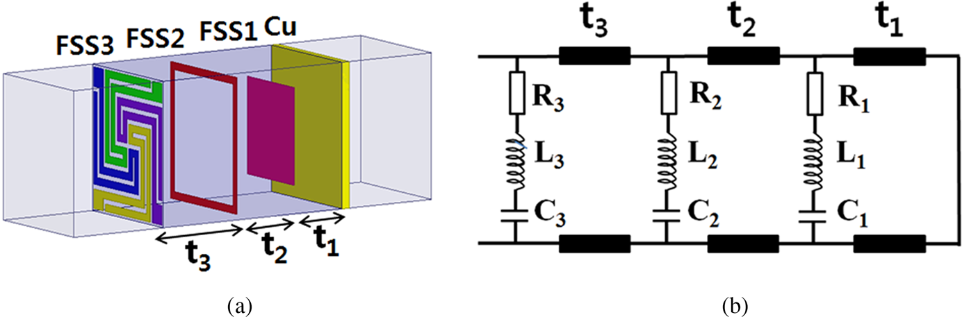
Reducing the size of the unit cell reduces the resonant frequency due to large values of capacitance among the conductors present in the entire circuit. These capacitances add up, thus lowering the resonant frequency and providing ultra-wide bandwidth. For this purpose, a high-capacitive multi-layered FSS with a new structure of folded spiral conductor was designed [Reference Liu and Kim55] as shown in Fig. 3. By combining a high-capacitive spiral FSS with other basic FSS structures such as the square loop and square patch, more than 90% absorption for 4.7–50 GHz was achieved. This was tested by free-space measurement of the sample fabricated using the screen printing method, which gave absorption in the bandwidth of 5.2–44 GHz for a thickness of 6.5 mm. For the single-layer FSS absorbers, the substrate was considered as air for simplicity, and reflection loss was measured for each of the absorbers. The S-FSS showed multiple absorption peaks at 6.8, 21.6, 37.8, and 40.4 GHz. The absorption peaks were shifted to higher frequencies such as 9.8, 30.5, and 53 GHz when the thickness was reduced from 9 to 7 mm. The spiral FSS with 100 Ω resistance and 2 mm thickness showed absorption in the 18.5–52.4 GHz frequency range. Due to the grating lobes, several smaller peaks of reflection losses were observed for frequencies larger than 50 GHz. The multi-layer FSS combines all three FSSs, to obtain better absorptivity.
Illustration of (a) triple-layered FSS absorbers with a combination of FSS1/FSS2/FSS3 (square patch/square loop/spiral) and (b) equivalent circuit. (Reprinted with permission from [Reference Liu and Kim55].)

Conventional millimeter-wave absorbers are thick and bulky where the performance is controlled by permeability and permittivity. While, in the case of MMAs, any variation in geometry could lead to improved performance. In general, the bandwidths of MMAs are typically narrowband, since it depends on the resonance bandwidth of the resonant structure [Reference Singh, Kabiri Ameri, Chao, Afsar and Sonkusale53].
Sun et al. [Reference Sun, Liu, Dong and Zhou30] proposed a broadband absorber using the concept of destructive interference. An MM with multi-layered split-ring resonators was used to obtain the desirable refractive index spectrum, which could induce anti-reflection in large bandwidth. The reflection from the two layers caused destructive interference, thus forming absorption. The resonances in ɛ and μ of the MM can be controlled to cause absorption of both electric and magnetic fields, which requires a resonator of a certain size and with low loss substrates. The successive anti-reflection causes large bandwidth absorption. However, despite using the SRR (split ring resonator), the resonance is not lossy enough to be called a perfect absorber but provides an optimum refractive index for causing destructive interference.
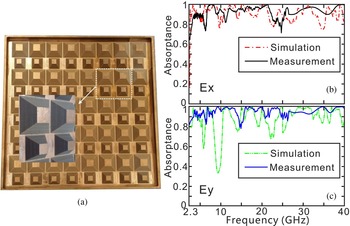
Multilayer resistive metasurface has also been used to develop broad absorption bandwidth and to achieve perfect impedance matching at resonant frequencies. Lumped elements or resistive films can also be used to obtain such broadband absorption [Reference Wang, Wang, Zhu, Yang, Kong and Liu7, Reference Batrakov, Kuzhir, Maksimenko, Paddubskaya, Voronovich, Lambin, Kaplas and Svirko28, Reference Yoo and Lim59, Reference Chen, Hu, Wang, Huang, Wang, Hu and Liu60–Reference Costa, Monorchio and Manara65]. Yin et al. [Reference Yin, Long, Li, Zhu, Chen, Guan and Li66] combined two dissimilar tapered hyperbolic metamaterial (HMM) waveguide arrays into a unit cell as shown in Fig. 4. Each of these waveguides has wide and dissimilar absorption bands. HMMs consist of metal/dielectric multilayers, possessing a large number of applications [Reference Zhang, Chen and Li67–Reference Salandrino and Engheta72]. After integrating these waveguide arrays, the broadband was achieved for the 2.3–40 GHz band, by varying the geometrical parameters and combining the absorption bands of the individual HMMs. This method is much preferred to discard the lower absorption bands that could appear in between the large bandwidth of the absorber.
(a) Fabricated sample of OS-HMM absorber. Simulated and measured absorption curves of OS-HMM absorber for (b) x polarization and (c) y polarization. (Reprinted with permission from [Reference Yin, Long, Li, Zhu, Chen, Guan and Li66].)

A similar study was conducted in 2014 by Li et al. [Reference Li, Wu, Wang, Zhai and Guan73] where they combined two layers of hybrid absorbers and obtained >90% absorptivity for the 4–40 GHz range. A triple layer topology of MMAs was proposed in [Reference Yahiaoui, Tan, Cong, Singh, Yan and Zhang74], comprising an array of resonators prepared from aluminum, deposited on the Kapton film substrate. This metal–dielectric–metal arrangement can be comprehended as a Fabry–Perot resonant cavity, where it helps in absorbing light between multilayered structures. The highly compact and flexible substrate helps in the integration of sensors on-chip.
Long and Zhiyong [Reference Li and Lv32] proposed an ultra-wideband absorber that consisted of three metasurface layers, having three resonant modes. The thickness of the absorber was designed to be 3.8 mm. The absorptivity measured was found to be more than 80% from 7 to 37.4 GHz. Here, the dielectric substrate was F4B-2. The applicability can be checked using different substrate candidates and comparing the absorption efficiencies with each other.
The three metasurface layers can be varied with different thicknesses and resistivity also. Improving the absorption performance of the Salisbury screen was achieved in [Reference Zhou, Chen, Zhao, Chen, Jiang, Zhu, Feng and Li75]. Here, the metasurface was used as the ground plane, rather than in the dielectric or the top layer of the absorber. The metasurface is capable of generating random phase responses and could control dispersion properties. This gives more degrees of freedom, helpful in broadening the bandwidth and good absorption performance of the conventional Salisbury screen. The absorption performance was studied for 6–30 GHz, with 133% fractional bandwidth, which was 85% better than a Salisbury screen with only 83% fractional bandwidth.
Some electronic applications require large light transmittance as well as absorbance. The optically transparent microwave system is an ongoing research area [Reference Lai, Wu, Zhu, Gu and Wu36]. In the past, an optically transparent MA for low frequency has been prepared. A millimeter-wave absorber has a different requirement for the structures.
Early in 1999, Takizwa et al. proposed a transparent absorber consisting of resistive sheets, ITO, and polyethylene terephthalate (PET) with polycarbonate (PC) as the spacer. They adjusted the sheet resistance of the top and bottom ITO layers to obtain absorption at 60 GHz [Reference Takizawa and Hashimoto37]. Thereafter, Soh et al. [Reference Soh, Kondo, Toyota and Hashimoto76] proposed the transparent absorber for two frequencies, 60 and 76 GHz bands. The absorber comprised of a dielectric spacer and three transparent resistive films prepared from PET and ITO, whereas the spacer was prepared from PC.
Lai et al. [Reference Lai, Wu, Zhu, Gu and Wu36] proposed an optically transparent ultra-broadband MA using ITO glass. ITO was used as the transparent conducting medium on the top and bottom of the glass material. The sputtering process allowed ITO to be deposited onto the glass substrate of 1.1 mm thickness. This was followed by wet etching to obtain the entire structure. The absorption ratio was verified by simulation and after fabrication and was obtained as >0.8 for 15.6–39.1 GHz.
A similar study [Reference Lai, Wu, Wang, Wu and Gu34] used ITO and PET as the material, with ITO on the top and bottom planes. An absorption of >0.8 was observed from 19.9 to 51.8 GHz. The thickness of the ITO film was 185 nm in both experiments [Reference Lai, Wu, Wang, Wu and Gu34–Reference Lai, Wu, Zhu, Gu and Wu36]. The analysis for the above was conducted for zero polarization angle of the incident EM wave. However, on changing the angle, it was observed that the absorption curve dropped for TM polarization faster than that of TE polarization. For θ ≤ 30°, the change in absorption spectrum was found to be negligible in both cases. Zhang et al. [Reference Zhang, Yang, Cao, Yuan, Ke, Yang, Cheng and Cui35] proposed an optically transparent absorber with a ring shape as the basic element, consisting of a sandwich structure prepared from ITO and polyvinylchloride along with PET. The observed absorptivity was from 26.5 to 40 GHz for angles between 0 and 60° for both the TE and TM modes.
A single-band ITO MM was designed by Yin et al. [Reference Yin, Lu, Gao, Yang, Lai, Li and Deng33] at 120.8 GHz with an absorptivity of more than 90%. This design being a single band, showed an interesting phenomenon, where, on changing the surface resistance of the ITO layers, one could observe characteristics of dual band also. This phenomenon could be used for applications requiring dual-band or more absorption techniques. Lu et al. [Reference Lu, Chi, Liu, Gao, Gao, Huang, Yang, Yin and Deng77] proposed an absorber based on tractable conductive plastic that was fabricated using three-dimensional (3D) printing, for 16.3–54.3 GHz frequency range with 108% fractional bandwidth.
Wu et al. [Reference Wu, Fu, Qian, Zong, Wu, Yue and Gu78] designed an optically transparent FSS-based absorber using a metal mesh structure and was fabricated using electrohydrodynamics printing technology. This method of printing is highly used in the area of millimeter-wave technology and is an economical technique with the capability of printing on pliant and flexible substrates. Due to the geometrical symmetry of the structure, polarization angle has no net effect on absorption. This property is useful for several applications.
3D absorbers
Another approach to develop absorbers with low weight and low cost are 3D MMs. These absorbers show very high absorptivity from microwave to visible spectra. Tang et al. [Reference Tang, Xiao, Xu, Ma and Wang48] proposed a 3D MMA prepared from nine resistive films of different sizes, mounted vertically on a metal plate. It showed an absorptivity of 90% for both TE and TM waves, in the 20–55 GHz frequency range. However, the proposed absorber was polarization-sensitive and can be used for polarization detectors, sensors, imaging, etc.
A 3D MMA consisting of resistive films and copper was designed, for normal incidence polarization, covering the 58.6–91.4 GHz frequency band. However, the design was complex and needed very careful precision while fabricating [Reference Tang, Xiao, Xu and Liu79]. Another multilayered, 3D structure was proposed by Ling et al. [Reference Ling, Xiao, Zheng, Tang and Xu49] which consisted of six resistive films placed on the ground plane. It consisted of mainly two layers, having six resistive films of different sizes, having square-shaped open rings. An ultra-broadband absorption was achieved from 38 to 142 GHz, with a wide incident and polarization angle.
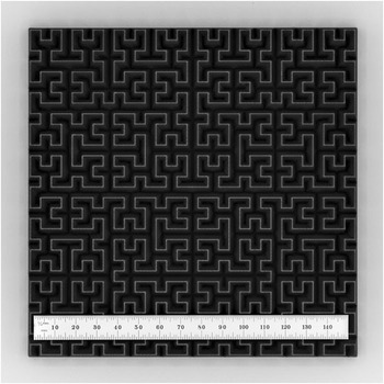
Vahidi et al. [Reference Vahidi, Rajabalipanah, Abdolali and Cheldavi80] designed a novel 3D absorber, having six-fold symmetry, consisting of a periodic honeycomb-like structure. The proposed design obtained more than 90% absorptivity in the 50–460 GHz frequency range. These designs were highly flexible, which could have applications extending to terahertz, infrared (IR), and visible ranges. They can be useful in imaging, sensing, and camouflaging technology. Petroff et al. [Reference Petroff, Appel, Rostem, Bennett, Eimer, Marriage, Ramirez and Wollack81] designed an absorber using an additive manufacturing process with a fused filament fabrication. The design was achieved using a Hilbert curve which is also known as the space-filling curve as shown in Fig. 5.
Prototype carbon-loaded HIPS Hilbert curve absorber. The footprint of the absorber is 160 mm square. (Reprinted with permission from [Reference Petroff, Appel, Rostem, Bennett, Eimer, Marriage, Ramirez and Wollack81].)

Another graded-index millimeter-wave absorber using a 3D printed mold was prepared by Adachi et al. [Reference Adachi, Hattori, Kanno, Kiuchi, Okada and Tajima82]. This mold had a pyramidal shape and absorbing material inside the mold. The unmolding step is not necessary if the 3D-printed mold is transparent within the millimeter-wave frequency range.
However, there is a limited option for the absorptive material to be selected in this case. Also, the advantage of this method was the optimization of thermal conductivity.
The advantage of using a 3D structure for absorption is its smaller unit cell size than the operating wavelength, as compared to the conventional 2D structures. This helps position it at the curved surface. It offers the ability to individually control the defined thickness of the designed unit cells. Therefore, it can counter the effects of curvature more flexibly [Reference Rashid, Li and Shen83].
However, 3D structures pose difficulty in the fabrication process, though, this can be compensated by its exceptional performance.
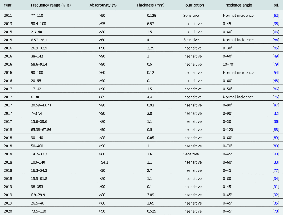
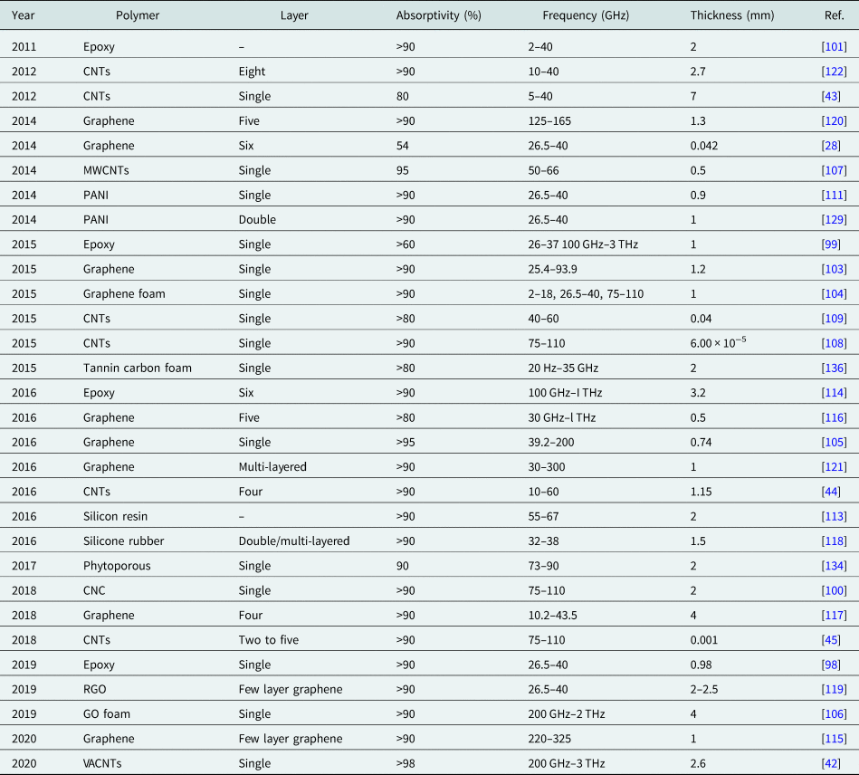
Table 3 shows the comparative study of the discussed millimeter-wave absorbers.
Comparative list of recently reported broadband millimeter-wave absorbers arranged in ascending order of year of publication

Based on polymer composites
Out of all the materials used in designing absorbers, the most popular has been the use of polymers, i.e. carbon-based materials. EM radiation can also interact with polymers through the most prominent absorption phenomenon. For frequencies <1 THz, EM waves are absorbed by those polymers which consist of polar groups, thus causing orientation polarization, which in turn generates heat. The absorption of IR radiation causes atomic vibrations, but there is no breaking of bonds, i.e. they do not undergo chemical reactions. However, visible and ultraviolet light interacts with inner shell electrons in the atom, undergoing chemical reactions. Even for frequencies higher than 1015 Hz, light interacts with shell electrons, causing chemical changes. The energy of a photon is thrice the magnitude lower than the binding energy in an atom. If sub-THz radiation is absorbed, there is a generation of heat, converting photonic energy to translational energy. This generation of heat is known as dielectric loss heating. This is because polar materials with permanent dipole moments are capable of absorbing sub-THz radiation. For absorption, EM radiation is an important measure to help in the synthesis processes of polymers via the polymerization of small molecules.
Some of the applications of the interaction of EM radiation with polymers are microwave heating useful for the vulcanization of rubber, recycling of polymeric waste, and industrial processing of polymeric materials [Reference Schnabel93]. Commonly used polymers for the development of millimeter-wave absorbers are graphene, CNTs, epoxy resins, and polyaniline (PANI). We will discuss these below.
Single-layered absorbers
Using epoxy resins. Epoxy resins are a very useful thermosetting polymer that are used as matrixes, with exceptionally good mechanical strength, chemical stability, heat stability, low contractibility, strong adherence, excellent electrical properties, dielectric constant, less shrinkage, chemical resistance, mechanical resistance, and a stable strength to weight [Reference Pitt, Barth and Godard94]. Epoxy resins are used for coating and sheathing the electrical circuit components where they protect the electrical devices from adverse effects of atmospheric changes, moisture, leaking current, mechanical shock, and vibrations. For the use of epoxy resins in electronics, the primary importance is of their dielectric constant which is 3–6 at normal temperature and low frequencies. Compared with other polymeric composites, epoxy is cheaper, easy to produce, and the amount of yield produced is in bulk, which can be used in several slots.
An absorber using epoxy-modified urethane rubber mixed with carbon particles was designed by Soh et al. in the range of 54–60 GHz [Reference Soh, Yoshioka and Hashimoto95]. In 2000, the authors designed an absorber using the same material, i.e. epoxy-modified urethane rubber mixed with carbon particles, and the absorption characteristics were calculated in the 50–110 GHz range, where the peaks were observed at 60 and 110 GHz [Reference Soh and Hashimoto96]. Similarly, the authors also proposed absorption peaks at 76 or 94 GHz bands using the same materials [Reference Soh, Yoshioka and Hashimoto97]. This was the earliest research study in the millimeter-wave range. Also, in 2003, the authors studied the absorption behavior of titanium dioxide (TiO2) and epoxy resin containing carbon particles. The absorption peak shows variation in the range of 50–110 GHz.
Here, epoxy resin is resistant to weather variations. The high permittivity of TiO2 and carbon particles proved to help design the absorber by satisfying the reflectionless conditions for absorption. In applications related to electronic packaging, it is challenging to achieve the requirements of EM wave absorption, namely (a) large reflection loss, (b) thin coating of the absorber, which would lessen the weight and thus, the cost also reduces (c) good compatibility with materials used for electronic packaging, so that it can be easily realized in the industry using epoxy resin or polyimide.
Xiao et al. [Reference Xiao, Chen, Hu, Xu, Deng, Niu, Li and Wang98] reported a novel epoxy-based absorber, where BNFO (BaNb0.6Fe11.4O19) was doped with epoxy and for electronic packaging applications. BNFO is used as a filler that can generate large dielectric and magnetic losses at once. Epoxy resin is used as a matrix since it is a typical material used for electronic packaging applications. As the BNFO content increased from 40 to 75 wt%, the improvement in matching conditions was observed with good absorption. The 60 and 75 wt% content of BNFO gave good absorption, with 13.5 GHz bandwidth in the 26.5–40 GHz range. The real and imaginary parts of permittivity increased as the content of BNFO increased. The real part of permittivity of epoxy is around 2.3, but it increased from 3.33 to 7.48, as the content of BNFO increased from 20 to 75 wt%. The imaginary part of permittivity of epoxy is 0.09, which increased from 0.32 to more than 2.25, as the content of BNFO increased from 20 to 75 wt%. A similar trend was observed for permeability also. The matching thickness showed a decrease from 1.09 to 0.97 mm as the content of BNFO increased from 40 to 75 wt%.
Due to the high weight content, the overall structure was bulky. Also, when the content of BNFO was above 40%, they observed a peak in the imaginary part of permittivity, which, though has been reported earlier, but is still under controversy and needs thorough investigation.
The epoxy resin composites filled with two types of commercially available graphitic particles, exfoliated graphite and thick graphite in 0.25–2 wt% was used in [Reference Bellucci, Micciulla, Levin, Petronyuk, Chernozatonskii, Kuzhir, Paddubskaya, Macutkevic, Pletnev, Fierro and Celzard99]. It was shown that epoxy composites of 1–2 wt% provided good EMI shielding both at microwave as well as THz frequencies. Though it was light weight, its absorption efficiency was quite poor.
Carbon nanocoil (CNC)-based composites were prepared by dispersion in epoxy resin through ultra-sonication with low concentration (0.1–1 wt%) by Suda et al. [Reference Suda, Matsuo, Yoshii, Yasudomi, Tanimoto, Harigai, Takikawa, Setaka, Matsuda, Suizu, Shima, Sandhu and Sharma100]. These novel CNC-based composites showed good absorption property in the W band (75–110 GHz). The solvent formed large agglomerations, causing irregularities on the absorber surface, making it difficult to maintain the thickness of the absorber constant. The effects of the chiral constant were not considered while deriving the permittivity, which can make it difficult to study the characteristic impedance of the absorber.
Epoxy resin was mixed with CNT and barium titanate (BT) fillers in [Reference Lozitsky, Vovchenko, Matzui, Oliynyk and Zagorodnii41] by Lozitsky et al., for 1–5 wt% of CNTs and 34 wt% of BT. Ferroelectric ceramics such as BT is commonly used to increase the dielectric parameters of polymeric composites. The absorber properties were studied from 1 to 67 GHz. The highest absorption was obtained for 10–65 GHz for 2 and 3 wt% CNTs.
The BaM + BaTiO3 with PANI composites was added as a filler into epoxy resin and polyethylene and synthesized via in situ polymerization process and was tested in the frequency range 2–40 GHz, where absorption bands were obtained at 9.6, 31, and 38.2. The magneto-electric effects caused the generation of electric and magnetic losses, and by the changes in the microwave field at the interface between the blend and polymer. The good absorption efficiency with the low cost and easier preparation mechanisms was observed in this case [Reference Yang, Gung, Shih, Hung and Wu101].
Using graphene. Currently, graphene is widely used in scientific research due to its properties such as high electrical and thermal conductivity and mechanical strength. The surface area of graphene is high, which makes them a good charge carrier. Graphene is a 2D structure of carbon connected in a covalent bond with the free-electron cloud of carbon which is perpendicular to the hexagonal plane. Due to this, there is a π–π interaction between the graphene sheets. But there may be the generation of several defects and dangling bonds, during the synthesis process. This leads to a lower intrinsic value of conductivity. These defects and dangling bonds result in the formation of different permanent polarization, which contributes to the absorption of EM waves. Though the defects and functional groups present in the graphene, at times limits the electrical conductivity, it has been still used for EM absorption purposes [Reference Pawar, Biswas, Kar and Bose102]. When graphene is mixed with polymers, the obtained composite has more advantageous properties than when it is used individually. The graphene composite forms a bond with each other to form a highly conductive system. Because of this, conductive losses can occur in the network. The microwave absorption process in graphene is a result of combined effects of polarization, conductive losses, interfacial, and multiple scattering. Graphene is tunable and has a surface impedance that is independent of frequency. This property is useful for impedance matching and thus, good absorption.
Zhu and Li [Reference Zhu and Li103] proposed a tunable wideband absorber that was designed using graphene patterns as an FSS placed on a dielectric substrate. By varying the conductivity of graphene, the absorptivity also changed. Setting the chemical potential to 0.3 eV, it was found that absorptance was 90% in 25.4–93.9 GHz. On expanding the unit cell, the working frequency was also observed to scale down.
Zhang et al. [Reference Zhang, Huang, Zhang, Chang, Xiao, Chen, Huang and Chen104] made use of a 3D free-standing graphene foam composite. That study reported enhanced absorption performance with a bandwidth of 50.5 GHz in the range, 2–18, 26.5–40, and 75–110 GHz. On tuning via physical compression, it has shown to change its absorption bandwidth, i.e. on 90% compression strain, it gives a bandwidth of 60.5 GHz, covering 93.8% of the entire bandwidth and about 70% wider than that of previously reported literature. The 3D conductive network of graphene foam can be used for applications of light and tunable high-performance absorption, such as electronic surveillance and stealth technology units with high payload.
Two-resistive patterned single-layered graphene was mounted on the dielectric substrate. It achieved absorptivity of 90% in 9.2–200 GHz [Reference Zhu, Li, Yin and Li105].
Ma et al. [Reference Ma, Chen, Hou, Huang, Huang, Xu, Fan and Chen106] showed the tunable and broadband absorption performance of 3D porous MXene/graphene oxide (GO) foam which covered the frequency range on the higher end of millimeter-wave, 200 GHz to 2 THz. A large number of nanometer porous structures cause multi-reflections of the EM waves. Introduction of MXene was shown to help in improving absorption performance. However, it was observed that when the ratio of masses of MXene and GO nanosheets are more than 1:5, absorptance does not increase.
Using CNTs. One of the important allotropes of carbon known as CNT or carbon nanotubes contains sp2 carbon, which has shown good EM wave absorption properties in the past. They have strong mechanical properties, with a tensile strength of 50–500 GPa and an elastic modulus value of 1 TPa. CNTs can be prepared to realize strong semiconducting properties and high charge mobility and current-carrying ability [Reference Danlée, Bailly and Huynen44]. CNTs are non-magnetic, thus, the absorption process originates from polarization, ohmic losses, or multiple scattering. Different types of CNTs, namely single-walled CNTs (SWCNTs) and multi-walled CNTs (MWCNTs) have been used as MAs in the past [Reference Gui, Wang, Wei, Lü, Shu, Jia, Wang, Zhu and Wu46].
Compared to SWCNTs, MWCNTs have larger defects due to their complex structure and large permittivity. Dielectric relaxation phenomena lead to absorption in this case. As the content of CNT increases, its percolation threshold affects its effective dielectric permittivity largely and hence the absorption characteristics.
MWCNTs can be added with non-woven fabric to achieve more than 95% absorption as shown by Sano and Akiba [Reference Sano and Akiba107].
A theoretical model was developed to study the characterization of nanomaterial by Nefedova et al. [Reference Nefedova, Lioubtchenko, Nefedov and Räisänen108]. To use this method numerically, it is important to study the material in a detailed manner. A CNT was placed randomly on a dielectric rod waveguide. It was measured from 75 to 110 GHz. Composite CNT films were studied in [Reference Wu, Cheng, Ma, Hu, Yin, Hu, Li, Yang and Xu109] due to their EMI-shielding effectiveness. The macro-films of CNT strongly adhered to the surface of the common cloth. This was obtained in the 40–60 GHz frequency range.
Using the properties of the waveguide of metallic honeycomb structure filled with PC foam and thermoplastic polyurethane reinforced with CNTs [Reference Quiévy, Bollen, Thomassin, Detrembleur, Pardoen, Bailly and Huynen43], absorption was obtained in the 5–40 GHz frequency range. For low weight content of CNTs dispersed inside the matrix, there is a good amount of attenuation. This is due to the aspect ratio which helps in the formation of a conductive network. However, it was difficult to achieve a good absorption index below 5 GHz, by keeping acceptable material thickness and cell size.
A graphene-vertically aligned CNT (G-VACNT) hybrid was proposed and designed for frequencies covering above 200 GHz to 3 THz [Reference Xiao, Zhu, Wang, Sun, Zhao, Ng, Teo, Hu and Tu42]. The absorber consisted of Cu/PDMS/graphene/VACNT layers placed upon the PET substrate. The VACNT is used for its low reflection with enhanced absorptivity at high frequencies. This structural arrangement was used for absorption at lower THz frequencies, from 200 GHz to 3 THz.
This can be highly flexible and can have wafer-scale fabrication. It can be used in applications such as bolometric imaging and energy harvesting.
Using polyaniline. PANI and its composites have been studied extensively in the past due to their microwave absorbing properties. They are inexpensive, easier to prepare, stable in both doped and undoped forms, have excellent chemical and physical properties, and good conductivity at microwave frequencies [Reference Dhawan, Singh and Rodrigues110]. The microwave absorbing properties of PANI originate from the fact that it is non-magnetic. The composites are prepared via polymerization techniques and mixing. Blending PANI with certain insulating polymers can improve the physical and chemical properties of PANI without any alteration in its structure. Among all the conducting polymers, PANI has shown a simpler synthesis process and environmental stability. PANI has been integrated with magnetic materials and conducting polymers [Reference Xu, Ma, Gan, Tang, Li, Zheng, Zhang, Xie, Yin, Shen, Hu and Zhang111, Reference Ćirić-Marjanović112].
The synthesis of the composite of chiral PANI and Barium hexaferrite (BF) was achieved in [Reference Xuan, Zhang, Zeng, Bo and Chan113] for the first time. BF is known to have a good magnetic property, also used in the development of MAs. But, when it is used alone, there is a large difference between the values of effective permittivity and permeability. This large difference creates impedance mismatch, thus reducing the effective absorptivity [Reference Xuan, Zhang, Zeng, Bo and Chan113].
Here, the composite developed was light weight, environmentally stable, and corrosion-resistant and the absorption above 90% was obtained for Ka-band. The good absorption was attributed to the balance between permittivity and permeability, due to the presence of both magnetic as well as dielectric elements.
Multi-layered absorbers
Using epoxy resin. A graded-index absorber was designed by Xu et al. [Reference Xu, Zhang, Zang, Sugihara, Zhao and Cai114]. The anti-reflection mechanism was achieved by tuning the dopant concentration of the polymer composites. To achieve a perfect reflection difference, the refractive index value of the matrix, epoxy resin was tuned by hollow PC microspheres and TiO2 nanoparticles. With a highly doped Si substrate and six layers of the structure, 98% absorption was achieved from 100 GHz to 20 THz.
Epoxy-based composites using graphene for 200–320 GHz were reported [Reference Barani, Kargar, Godziszewski, Rehman, Yashchyshyn, Rumyantsev, Cywiński, Knap and Balandin115], where the transmission was found to be very less, even at small concentrations of fillers. The higher doping concentration of graphene improves the heat conductivity properties, but on the other hand, also increases reflections. So, it is important to scale the graphene content as much as to improve the heat conductivity without any increase in reflection. Here, the graphene content was low, which ensured the low cost of the absorber. The absorptivity of more than 95% is achieved when the content of graphene was 1 wt%.
Using graphene. Batrakov et al. [Reference Batrakov, Kuzhir, Maksimenko, Volynets, Voronovich, Paddubskaya, Valusis, Kaplas, Svirko and Lambin116] used the inclined geometry that increased the conductivity of graphene films, and compared the two possible dielectrics, quartz and epoxy as the substrates for the maximum absorptivity. The absorptivity of 80% was obtained at 30 GHz and 65% at 1 THz.
Liu et al. [Reference Liu, Yuan, Yuan, Wei and Yuan117] designed a thin absorber by placing a Jerusalem-shaped patch prepared from graphene in between the dielectric layers. The unit cell consisted of four layers, a graphene-resistive pattern, and two dielectrics, having the same thickness and permittivity, and a ground plane. It was shown that with an increase in the permittivity of dielectric slabs, the bandwidth decreases but there is hardly any change in the fractional bandwidth. An increase in the thickness of the substrate decreases the bandwidth and fractional bandwidth. It was shown that when the permittivity (ɛr = 2), the wide absorption was obtained from 10.2 to 43.5 GHz with the fractional bandwidth of 124%.
The design was bulky and that as the chemical potential is increased, bandwidth increases but at the cost of absorptivity. A composite of magnetic iron particles and expanded graphite was prepared by Hung et al. [Reference Hung, Cheng, Lan, Chang and Wu118]. It is to be reminded that graphite is composed of several layers of graphene. In the above case, the composite gave good attenuation properties in 32–38 GHz.
Chen et al. [Reference Chen, Fu, Liu, Zhang, Cao, Yuan and Liu119] designed an excellent millimeter-wave absorber for 5G applications, where elastic absorbing composites were fabricated using reduced graphene oxide (RGO) with different reducing times along with nitrile butadiene rubber (NBR). The dihedral angles formed by the stacks of RGO sheets cause multiple reflections thus, laying the foundation of a good absorption mechanism. The RGO/NBR composites with a reduction time of 3, 5, 7 h were prepared, out of which 3 h-RGO/NBR exhibited the best absorption performance at 35.4 GHz. The study was conducted for the Ka-band.
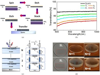
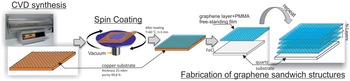
Wu et al. [Reference Wu, Tuncer, Naeem, Yang, Cole, Milne and Hao120] reported the fabrication of transparent absorbers, consisting of multilayered graphene sheets, put on top of a quartz substrate with a grounded metal plate. The graphenes were prepared using the chemical vapor deposition method. The multilayered graphene sheets were produced by the repeated procedure of etching and transfer as shown in Fig. 6. This method was used to minimize the PMMA residues and thereby producing high-quality and optically transparent graphene films. It is important to note that, each graphene–quartz layer forms a Fabry–Perot resonator. When the graphene–quartz samples are layered together, they form a mutual coupling, which gives rise to multiple absorption peaks, hence creating broadband. On verifying it experimentally, it was found that for five layered structures, 90% absorption efficiency was obtained from 125 to 165 GHz, with a fractional bandwidth of 28%. However, a thin-layered graphene absorber could be developed, with relatively less cost. Also, different structural absorbers could be realized to study the EM properties. Batrakov et al. [Reference Batrakov, Kuzhir, Maksimenko, Paddubskaya, Voronovich, Lambin, Kaplas and Svirko28] demonstrated in his work, that sandwiched PMMA thin films between the graphene layers have very good absorption efficiency. This was done for the frequency range of 26.5–40 GHz. At around 30 GHz, the absorption was highest when the number of graphene layers was six. Increasing the number of layers reduced the absorption efficiency. Using a small thickness layered structure with high absorption would be applicable for nanodevices. PMMA/graphene multilayers have proven to be flexible shielding materials. The process of preparation is shown in Fig. 7.
(a) Representation of an etch and transfer preparation process for a two-layered device, (b) UV-Vis spectra for 1–4-layered graphene samples, (c) schematic representation of the N layered absorber with its equivalent circuital model, and (d) optical images of 2 and 3 layered absorbers and N = 1 to 4 graphene-quartz stacked samples. (Reproduced with permission from [Reference Wu, Tuncer, Naeem, Yang, Cole, Milne and Hao120].)

Representation of graphene sandwich fabrication, with several repeating steps and final PMMA/graphene structure, is formed. (Reproduced with permission from [Reference Batrakov, Kuzhir, Maksimenko, Paddubskaya, Voronovich, Lambin, Kaplas and Svirko28].)

This was further improved by Mencarelli et al. [Reference Mencarelli, Pierantoni, Stocchi and Bellucci121] who proposed multi-layer PMMA/graphene for high-EM absorption in the millimeter-wave frequency range. The optimization was done by properly patterning the multi-layered structure. The graphene layers were perforated with holes of a controlled radius.
The average conductance of the graphene layers was varied and absorption efficiency was measured. For the conductance of 0.8 mS, absorption of more than 75% was observed with small ripples as compared to the conductance of 0.3 mS, with 100% absorption and a large number of ripples. The designed absorber has been reported for use in innovative surface and coatings, not only absorption.
Using CNTs. Danlee et al. [Reference Danlée, Huynen and Bailly122] used PC and CNT to design an MMA. A good absorber needs to have antagonistic properties, meaning, it must have a certain conductivity level along with a low dielectric constant. Since these properties are not found naturally, these can be designed artificially, which was done by Danlee et al. They designed a thin and flexible absorbing solution, which could be used to isolate any electronic, medical devices from EMI. They used PC to homogeneously disperse CNT. The shape of CNT helps in lowering the percolation threshold to a smaller percentage of weight. Absorption of above 80% was observed for 10–40 GHz. This method showed an arrangement of successive dielectric and conducting layers, to create a conducting gradient. This method can be used for higher frequencies, with modifications in thickness and conductivity.
This study was extended and applied by the authors in [Reference Danlée, Bailly and Huynen44] where the applicability of the gradient-multilayer method was extended in that study by patterning the conductive layers as strip lines, which thereafter induces strong anisotropy leading to a good absorption property. The designed absorber was polarization-dependent, using CNT deposited on PC sheets. However, the main requirement of this absorber was that the ratio between gaps between conductive strip lines to its width must be 5.
Biswas et al. [Reference Biswas, Panja and Bose123] designed a millimeter-wave absorber by choosing a polymeric blend of immiscible solution of PC and polyvinylidene difluoride. To achieve absorption of EM wave radiation, the two most important key factors, high conductivity and large loss characteristics were achieved by incorporating MWCNTs. The addition of magnetic Fe3O4 clusters exhibited efficient heat dissipation, high absorptivity due to the presence of electric and magnetic dipoles, making it suitable for developing millimeter-wave absorbers.
Using a metallic waveguide structure for embedding CNT-based absorbers [Reference Anoshkin, Campion, Lioubtchenko and Oberhammer45] using various preparation methods is also important in determining its usefulness. Here, the experiment was held for 75–110 GHz, where the absorber which was a CNT-based material was highly porous aerogel, prepared by freeze-drying technique.
The advantage of this method is that the porous structure formed has random orientations and offers low surface reflections, hence enabling effective absorption. This method of preparation can be extended beyond THz applications.
Combining CNTs with cement was achieved [Reference Hirose and Ono124] where the cement matrix of the absorber has electrically conductive paths, which are isolated from each other and a CNT forms a resistor/capacitor structure with excellent dielectric behavior.
Using polyaniline. The new composite materials formed have improved applications and properties in microwave absorption. M-type BF (barium ferrite) is a potential material for microwave absorption since it has large magneto-crystalline anisotropy, large magnetization, and Curie temperature [Reference Yu and Huang125]. The electric and magnetic properties must be modified to obtain improved properties. Ting and Wu [Reference Ting and Wu126] synthesized PANI/Ba ferrite composite via in situ polymerization method. Good absorption properties were exhibited in the frequency range of 2–40 GHz. This composite was synthesized via in situ polymerization and showed excellent millimeter-wave absorption properties in the range of 2–40 GHz. Magnetite (Fe3O4) has not only the strongest magnetic properties, but it also has excellent EM-absorbing properties [Reference Gu, Huang, Zhang, Wang, Zhu, Shao, Haldolaarachchige, Young, Wei and Guo127].
Belaabed et al. [Reference Belaabed, Wojkiewicz, Lamouri, El Kamchi and Lasri128] showed that addition of magnetite dopants improves the EM-absorbing properties of the PANI composite. Xu et al. [Reference Xu, Ma, Huo, Gan and Tang129] designed a double-layered millimeter-wave absorber with PANI and PANI/Fe3O4, where PANI was a matching layer and the latter was an absorbing layer, the absorption efficiency was highest at 33.72 GHz. The total bandwidth was 11.28 GHz, with a frequency from 27.24 to 38.52 GHz. Bamboo charcoal coated with PANI was prepared at different weight ratios and introduced into epoxy resin. At higher weight content, the electrical conductivity of BC/PANI increased, implying that PANI improves electrical conductivity. These composites exhibited good absorption performance in the range of 2–40 GHz. The difference in the absorption peaks implies the dielectric and magnetic loss which was generated by the magnetic dipoles and by the change in boundary condition of the microwave field at the interface of the prepared composite and the polymer matrix [Reference Wu, Ting, Wang, Yang and Tsai130]. Few rare-earth elements have been added to PANI to observe a good absorption efficiency [Reference Xudong, Jianjiang, Baocai, Hongfei and Xingjian131].
Yu et al. [Reference Zhang, Wang and Zhou132] developed cerium oxide doped in PANI/Al-alloy foams with doping of cerium oxide in 1, 2, and 5%. This showed excellent absorption in 12–18 and 26.5–40 GHz. Yu [Reference Yu133] developed another rare-earth doped in PANI/Al-alloy foams as a composite material to develop the absorber in 12–18 and 26.5–40 GHz. The absorption increased by increasing the frequency. The rare-earth doped in PANI did not change the shape of PANI, as was observed in the scanning electron microscopy images, indicating the uniform dispersion of the particles. The absorption of pure PANI, 2% doping of rare earth, and 5% doping, increased with the increase of frequency.
Conclusion
This review provides an insight into the progress in the development of millimeter-wave absorbers and challenges faced by microwave/RF designers. The development of low-cost, thin, and polarization-independent absorbers with maximum efficiency has been shown. It primarily focuses on the classification of geometrical as well as material-based designing of the broadband millimeter-wave absorbers with their shortcomings as well as their applications. Polymeric composites have been shown to find application in the development of flexible and tunable absorbers. Various polymer composites such as CNTs, graphene, epoxy resins, and carbon gels have been used to develop absorbers in the millimeter-wave frequency range. Compared with conventional EM absorber polymeric materials, the highly demanded 3D graphene guarantees promising results in EM wave absorption. When graphene is combined with polymers, the formed composites add precedence not only in the EM-absorbing ability, but also they are low weight, flexibility, and low cost.
Agricultural residues which are not suitable for human consumption have also been used for developing millimeter-wave absorbers [Reference Kamei, Shima, Yamamoto, Ogino and Ishii134]. These residues preserve properties such as light weight, high heat retention, good absorptivity, and high permittivity, which are the primary requirements for developing high-quality absorbers. Absorbers using such residues have not been used much for the millimeter-wave frequency band. Some carbon-based magnetic composites have been used for EM absorption in the lower gigahertz range. Very few studies have been conducted for the millimeter-wave range, using carbon-based magnetic composites [Reference Liu, Itoh, Horikawa, Machida, Sugimoto and Maeda135]. Absorbers using silicon resin [Reference Xuan, Zhang, Zeng, Bo and Chan113] and tannin [Reference Letellier, Macutkevic, Paddubskaya, Plyushch, Kuzhir, Ivanov, Banys, Pizzi, Fierro and Celzard136] have also shown good absorption efficiency. Table 4 shows the comparative study of the various polymeric millimeter-wave absorbers discussed in this paper.
Comparative list of recently reported polymeric millimeter-wave absorbers arranged in the ascending order of year of publication

For different frequency bands in the EM wave spectrum, there are various applications of millimeter-wave absorbers. These absorbers have found use in diverse areas of technology, though initially it was used for concealment and enhancing radar efficiency. These are widely used in the defense sector, where there is a need to develop radar-absorbing materials and improving the radar characteristics.
The radar-absorbing materials are widely used in stealth technologies and as EMI shielding for high reflection surfaces. The stealth technology is the most typical application of EM wave absorption. This method is useful for escaping the detection of aircraft by reducing the radar cross-section area. Other electrical applications include reducing the negative impacts of cavity resonance in the integrated microwave circuits, thermal sensors [Reference Sen, Islam, Banerjee and Das137], healthcare [Reference Lee, Kim and Lim138], and frequency-related sensors [Reference Asadchy, Faniayeu, Ra'di, Khakhomov, Semchenko and Tretyakov139]. Several of the electronic appliances use absorbers in their circuits for diversified uses such as amplifiers [Reference Hamm, Wuestner, Tsakmakidis and Hess140], filters [Reference Asadchy, Faniayeu, Ra'di, Khakhomov, Semchenko and Tretyakov139], switches [Reference Hajizadegan, Ahmadi and Sakhdari84], and bolometers [Reference Landy, Sajuyigbe, Mock, Smith and Padilla3]. It is also used in high rising buildings, for prevention of EMI, for preventing leaking waves of the microwave oven, for protection of local area networks, and in anechoic chambers. These are also used for developing isolation in electronic devices and mobile communications [Reference Li, Gao, Cao, Zhang, Liu, Zheng, Zhang and Zheng85–Reference Wu, Deng, Wang, Zong, Chen and Gu92, Reference Assimonis and Fusco141].
 Anupriya Choudhary currently works as a Ph.D. scholar in Electronics and Communications Engineering department at BIT Mesra, Ranchi. She has obtained her M.Tech. from BIT Mesra in Nanoscience and Nanotechnology in 2017. She has completed her B.Tech. from Electronics and Communications Engineering department at MIT Manipal, Karnataka in 2015. Her research interests include absorbers, metamaterials, frequency selective surfaces (FSSs), and materials’ characterization.
 Srikanta Pal received his B.Tech. from NIT Warangal. He received his M.E. degree from Jadavpur University and his D.PHIL. from Oxford University. He is currently working as a professor in the ECE department at BIT Mesra, Ranchi. He has 8 years of experience in the industry and 22 years in research around the globe. He has teaching experience of more than 15 years. His research interest includes antennas, filter synthesis and analysis, metamaterials, microwave/terahertz imaging and sensors, statistical signal processing, radio astronomy, fractals, EBG/PBG, DGS, reconfigurable geometries and frequency selective surfaces (FSSs), computational electromagnetics, thin film-based wireless components using high-temperature superconductors, ferroelectrics, etc.
 Gautam Sarkhel is currently the Head of Department and Professor of Chemical Engineering Department, BIT Mesra. He completed his B.Tech. in 1998 from Calcutta University. Thereafter, he completed his M.Tech. from IIT Delhi in 1999 and his Ph.D. from Jadavpur University in 2006. He has more than 19 years of teaching and research experience at BIT Mesra, Ranchi. His research interests include polymer composites, surface coating, membrane science and technology, reactive polymer blends, specialty polymers and membranes for fuel cells, etc.