I. INTRODUCTION
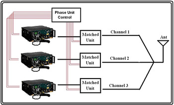
Multiple communication channels, commonly found in control centers, suffer from the problem of limited space and cost resources. In the case of mobile command centers, the lack of space is even more problematic, and limits the number of possible communication systems. Moreover, in military applications, a dense antenna setup can put RADAR invisibility at risk. Combining several channels to single output antenna, with no matching solutions, will result in distractive interference between the channels and a significant loss in transmission output. Possible solutions to this matching problem are already available, such as Triplexer or Splitter/Combiner units. However, such solutions have disadvantages such as fix frequencies (Triplexer) [Reference de Assuncao, de Menezes and Abdalla1], or inherent insertion loss (5 dB in a three-channel combiner) [Reference Wilkinson2]. In order to obtain a frequency tuned, low insertion loss, and low return loss matching unit, we have developed a Multi-Channel Phase Control system (MCPC), allowing the simultaneous transmission and receiving of several channels through a single antenna, as shown in Fig. 1. Our MCPC allows the reduction of antenna number by a factor of three.
Three channels coupling system connected to a single antenna using three phase-shifting units.

II. MCPC SYSTEM DESIGN
A) System configuration
The proposed system was designed for a frequency range of 30–80 MHz (VHF Band). The phase matching is obtained by a capacitor-tuned phase shifter. We required the phase shifter to meet the following specifications: insertion loss lower than 3 dB and S 11 lower than −20 dB. Therefore, we chose to implement the phase shifter design with a hybrid 90° coupler and a capacitor bank installed in each channel. In order to achieve matching between the three channels, the system is computer controlled (Fig. 1), determining the precise capacitor values. As a result, each channel is matched for a specific frequency band, while the other channels are kept isolated.
B) Coupler
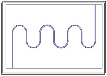
The coupler was designed in a stripline structure for uniform transverse electromagnetic (TEM) wave propagation. Accordingly, the coupler can be modeled as an equivalent capacitor circuit [Reference Collin3, Reference Pozar4]. The design must take into consideration a wideband matching range and high-power transmission within acceptable dimension limitations for acceptable application. To achieve small-scale device in this frequency range, we selected meander geometry [Reference Weiss5–Reference Sugiura7]. We used electromagnetic simulations in order to design our coupler. Taking into account the contribution of even and odd modes of the coupler, we used the following equations:
 $$Z_{0_o} = {\eta _0} \displaystyle{1 \over {2W\sqrt {\varepsilon _r} \left[ {\displaystyle{{2B} \over {{B^2} - {S^2}}} + \displaystyle{1 \over S}} \right]}},$$
 $$Z_{0e} = {\eta _0}\displaystyle{{{B^2} - {S^2}} \over {4BW\sqrt {\varepsilon _r}}}, $$
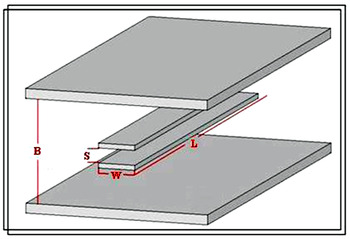
where Z 0 o and Z 0 e are the approximate odd and even mode impedance expressions, respectively, B is the distance between the two ground plates, S is the distance between the two strip lines, W is the strip width, η 0 is the characteristic impedance of free-space, and ε r is the relative dielectric constant of the substrate. The stripline geometry and the related parameters are shown in Fig. 2. The total impedance Z 0 of the coupler [Reference March8] can be written as
 $$Z_{0} = \sqrt {Z_{{0_e}}{Z_{0o}}}. $$
Stripline coupler.

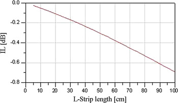
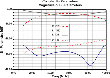
In the following section, we will elaborate on several considerations which must be taken into account for design of the mentioned coupler geometry [Reference Rehnmark9]. First, line width affects both mutual coupling and impedance value. In our simulation, the line width, which was first designed to be uniform, exhibited undesired mutual coupling and high electrical fields close to the coupler ports. Second, the bending radius of the meander must be larger than the strip width [Reference Pozar4]. In our simulation, the coupler dimensions exceeded the maximum dimension constraints due to high bending radius to strip width ratio. Therefore, a correlation between W and S was introduced into the coupler design, and simulated to maintain the typical impedance and a minimal power loss. Finally, the distance between the two parallel lines must be large enough to achieve a minimal mutual coupling while retaining the compact dimensions of the coupler. Moreover, long parallel lines contribute to undesired mutual coupling along the stripline. Therefore, simulations of the power loss as a function of line length, line width, and line separation were performed (Fig. 3) in order to obtain optimal line dimensions. In addition, our coupler design was based on commercial materials in order to enable a future device fabrication. The simulation was based on the RT/duroid 6006 substrate with a relative dielectric constant of 6.15 and a thickness of 9.51 mm with 2 Oz of the copper layer. In order to obtain our device geometry, we introduced a combination of two striplines separated by the RT/duroid 6006 substrate with a thickness of 1 mm, B = 20 mm, S = 1 mm, W = 3, and L = 550 mm as defined in Fig. 2. Additional substrates were combined in order to obtain the device thickness requirements from the stripline to the ground plates. Electromagnetic simulations of the hybrid coupler show an insertion loss of ~3 dB in the transmission and coupling ports along with a reflection coefficient (S 11) lower than −20 dB at the frequency range of 40–75 MHz (Fig. 4). The final structure of the coupler is shown in Fig. 5.
IL (dB) as a function of stripline length (cm).

S-parameters HFSS simulation of the coupler. Port designation: 1 for input, 2 for coupling, 3 for through, and 4 for isolation.

Meander geometry of the coupler showing six bends structure with steps in the width along the line.

C) Capacitor bank
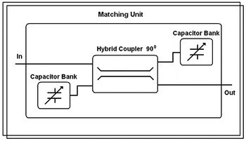
The capacitor bank was connected to the coupling and to the through ports of the coupler, as a part of the matching unit diagram block, shown in Fig. 6. The capacitor bank, covering a phase range of 0–180°, was monitored by a phase control unit, which determines the capacitance for each channel. Each capacitance value provides a specific phase shift at a given frequency. The obtained phase shift was correlated with the two other channels to maintain a simultaneous phase match to the antenna. In order to obtain the capacitance value for each channel, the following procedure was applied, starting with equation (4), which represents the matching condition for couplers junction, in our case it was realized for three channels.
 $${\mathop{\rm Im}\nolimits} \left\{ {\;\sum\limits_j {{y_{ij}} + {y_{st{b_i}}}}} \right\} = \sum\limits_j {{b_{ij}} + {b_{st{b_i}}} = 0}, $$
 $${y_{ij}} = \displaystyle{{1 + {\Gamma _{ij}}} \over {1 - {\Gamma _{ij}}}}.$$
Matching unit diagram block.

y ij and Γ ij are the admittance and reflection coefficients, respectively, of channel j at the (self)-frequency of channel i. y stb i is the admittance, at the (self)-frequency of channel i, of the additional stub connected between the matching unit and the junction of the three channels. By equating the imaginary part of the admittance to zero we can extract b ij , the susceptance of channel j, at (self)-frequency of channel i and b stb i , the susceptance of the additional stub at the self-frequency of channel i. By equating this part to zero, we can state that the junction is matched for all connected channels. The reflection is given by
 $${\Gamma _{ij}} = {\langle {{S_{11}} + \displaystyle{{S_{21}^2 {\Gamma _B}} \over {1 - {S_{22}}{\Gamma _B}}}} \rangle _{ij}},$$
where Γ B is the reflection coefficient of the stub. The reflection coefficient is obtained from the S-parameter matrix of each channel. Using the junction equation [Reference Collin3, Reference Pozar4], and assuming a system of three channels, we can write the following matrix equation:
 $$\eqalign{{b_{{\rm 12}}}({C_2}) + {b_{{\rm 13}}}({C_3}) + {b_{st{b_1}}} & = 0, \cr {b_{{\rm 21}}}({C_1}) + {b_{{\rm 23}}}({C_3}) + {b_{st{b_2}}} & = 0, \cr {b_{{\rm 31}}}({C_1}) + {b_{{\rm 32}}}({C_2}) + {b_{st{b_3}}} &= 0.} $$
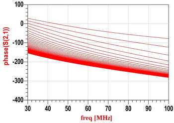
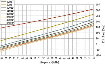
C i is the capacitance value for coupler in channel i and bij(C i ) is the susceptance as a function of the associated capacitance. This matrix is solved numerically and results in a nine capacitors bank with capacitance range of 10–500 pF. The capacitance of each channel is found derived numerically, based on prior knowledge of the other channel frequencies. A typical phase shift graph, as a function of frequency, for several capacitance values, is shown in Fig. 7.
Phase shift simulation of coupler with a capacitors bank. The figure shows different phase shift lines for capacitors ranging from 10 to 500 pF where the calculating, up line, curve are related to the highest capacitance. The phase shift is linear along the frequency and exhibits a phase of more than 180°.

III. SYSTEM OPERATION & SIMULATION RESULTS
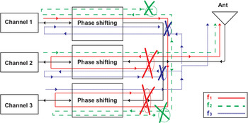
The different capacitances, each connected to a different channel, determine the phase shift obtained by the reflection from other channels. To demonstrate our design, a schematic block diagram of the propagating and reflected waves is shown in Fig. 8. In this manner, a propagating wave from a transmitting system accumulates phase along the transmission lines and the phase shifter up to the junction point. With a multi-channel system, one must take into account the reflection of the propagating wave from each of the other channels. The reflected signals from the other two channels interfere destructively with the original one at the junction point. Therefore, each channel is matched to the antenna, while other ports are considered to be open, i.e. having high impedance. This analysis can also be performed in the opposite direction, i.e. receiving analysis, and results in the same mechanism, due to reciprocity.
Propagating wave in the full multi-coupler system demonstrates interferences at the junction point.

The system operation was simulated using Agilent ADS software in order to check our design. In the simulation, the coupler S-parameters were obtained from the electromagnetic simulation results. First, we had to simulate the S-parameters of the phase shifter block, in order to obtain the susceptance coefficients for the junction equation. The system simulation was carried out for the three channels, each working at a different frequency. The three sources were connected to output band pass filters of BW = 5 MHz in order to simulate an actual communication system.
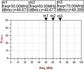
The capacitance value for each channel was calculated in order to obtain matching to the junction point. The harmonic balance simulation, as seen in Fig. 9, shows the original output power of each channel at the junction point without reflection interferences. Our simulation shows an insertion loss of approximately 0.5 dB in each channel.
Simulation of the full multi-channel system. ADS simulation shows transmission of 50 dBm output power in three different operating frequencies: 50, 60, and 70 MHz. Simulation shows the maximum insertion loss of 0.6 dB.

A) Experimental results
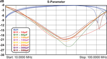
Measurement was performed on the coupler and a two continuous bank capacitor, having a capacitance range of 10–350 pF. Ports 1 and 2, respectively, are the phase shifter, input, and output ports (Fig. 6). Figure 10 shows the phase shifter scattering coefficients for different capacitance values.
Matching unit scattering coefficients.

The blue graphs indicate the transfer coefficients for different capacitance values. Insertion loss (IL) measured on the device, in the relevant frequency range, was −0.5 dB. Reflectance coefficients for the input port are marked in different colors corresponding to different values of capacitance.
Figure 11 presents the capability of the phase shift unit. The graph shows a linear frequency behavior for each capacitive value, for the 35–80 MHz frequency range. The capacitor bank, with a capacity range of 10–350 pF, provides phase shift ability of 180°. This behavior facilitates the computation of the system and displays a monovalent value for channels matching.
Phase control capability for different capacitance values.

IV. CONCLUSION
We designed and implemented a multi-channel matching system, based on a phase shifter, for three simultaneous communication systems. We demonstrated that the design meets the primary requirements for minimum insertion losses and return losses in each channel. Using our design, it is possible to reduce the number of antennas by a factor of three, without compromising the system performance. A phase-shifting capability of 180° is demonstrated, along with low IL of about −0.5 dB per channel.
ACKNOWLEDGMENT
This work was supported in part by the Israeli Ministry of Defense (grant number 802676).
 Eldad Holdengreber received his B.Sc. and M.Sc. degrees from the Department of Electrical and Electronic Engineering of Ariel University, Israel, in 2008 and 2012, respectively. Currently, he is working toward his Ph.D. degree. His research interests include designing superconducting microwave circuits and microcontrollers applications. His present research deals with THz detector based on Josephson junction.
 Moshe Mizrahi received his B.Sc. degree in 2008 and his M.Sc. in 2011 from the Department of Electrical and Electronic Engineering of Ariel University. Since 2007 he has been a Research Assistant in the Department. His research interests include designing microwave passive circuit based on superconductors. He is a Ph.D. student in Bar-Ilan University and his present research deals with Radar Super Resolution problems.
 Elichai Glassner received his B.Sc. degree in 2009 in the Department of the Electrical and Electronic Engineering of Ariel University. Currently he is an M.Sc. Student. Since 2009 he has been a Research Assistant in the Department. His research interests include RF and Microwave.
 Yoav Koral received his B.Sc. and M.Sc. degrees from the Department of Electrical and Electronic Engineering of Tel-Aviv University in the years 1982 and 1990, respectively. From 1982 he is with the Elisra Electronic Systems Company working as a research and development engineer specializing both with RF and Microwave interest together with the Control interest.
 Shmuel Schacham Professor Schacham, Dean of Students of Ariel University, is the founder of the Department of Electrical and Electronics Engineering. He served as a Dean of Engineering for 14 years. His main research interests include microelectronics, infrared detectors, quantum electronics, and microwaves.
 Eli Farber received his M.Sc. degree in Electrical Engineering and Ph.D. degree in Physics from Tel-Aviv University, Israel in 1997 and 2001, respectively. In 2002, he joined Ariel University, Department of Electrical and Electronic Engineering as a faculty member. He is a head of the laboratory of Superconductivity and Optical/Microwave Spectroscopy. His main research interests include RF/microwave devices, such as directional couplers, antennas and filters for wireless communications, millimeter and submillimeter-wave heterodyne and direct detector receivers, frequency sources in the terahertz region, antennas, imaging and spectroscopy, novel microwave and IR materials, high-temperature superconducting electronics, micro/nano fab-rication, and processing.