
I. INTRODUCTION
Organic–inorganic halide perovskite solar cells (OIHPSCs) show promise as renewable energy sources in the future. Reference Snaith1–Reference Bae, Zhao, Hsieh, Zuo, De Marco, Rim, Li and Yang4 A distinct feature with OIHPSCs is their combined merits of low-cost solution processability and extraordinary optoelectronic properties, including long carrier lifetime, Reference Stranks, Eperon, Grancini, Menelaou, Alcocer, Leijtens, Herz, Petrozza and Snaith5 large absorbing coefficient, Reference Green, Ho-Baillie and Snaith6 high tolerance for trap states, Reference Oga, Saeki, Ogomi, Hayase and Seki7 and high dielectric constant. Reference Bae, Zhao, Hsieh, Zuo, De Marco, Rim, Li and Yang4,Reference Lin, Armin, Nagiri, Burn and Meredith8,Reference Juarez-Perez, Sanchez, Badia, Garcia-Belmonte, Kang, Mora-Sero and Bisquert9 Within a quite short time span, the device performance of perovskite solar cells was rapidly improved from 3.8% (2009) Reference Kojima, Teshima, Shirai and Miyasaka10 to 22.7%, Reference Yang, Park, Jung, Jeon, Kim, Lee, Shin, Seo, Kim, Noh and Seok11 as a result of intensive research on compositions, Reference Jung and Park12,Reference Jeon, Noh, Yang, Kim, Ryu, Seo and Seok13 device architecture designs, Reference Jeon, Noh, Kim, Yang, Ryu and Seok14 morphologies, Reference Eperon, Burlakov, Docampo, Goriely and Snaith15,Reference Zuo, Dong, De Marco, Hsieh, Bae, Sun and Yang16 and interfacial engineering. Reference Zhou, Chen, Li, Luo, Song, Duan, Hong, You, Liu and Yang17
The structure of the perovskite active layers can be described as ABX3, where A is a cation, e.g., methylammonium (MA+), formamidinium (FA+), Cs+, etc., B is a metal cation, e.g., Pb2+, Sn2+, etc., and X is an anion, e.g., I−, Br−, Cl−, SCN−, etc. Reference Jung and Park12,Reference Chen, De Marco, Yang, Song, Chen, Zhao, Hong, Zhou and Yang18,Reference Cheng and Lin19 To form a stable three-dimensional (3D) structure, the selection of component ions can be predicted by the Goldschmidt tolerance factor, t,
 $$t = {{{R_{\rm{X}}} + {R_{\rm{A}}}} \over {\sqrt 2 \left( {{R_{\rm{X}}} + {R_{\rm{B}}}} \right)}}\quad ,$$
where R A, R B, and R X are the radius of A, B, and X ions. It was revealed that a cubic perovskite is formed when 0.9 < t < 1, while a hexagonal or tetragonal structure is formed with t >1 and an orthorhombic or rhombohedral structure is formed with 0.71 < t < 0.9. Reference Saliba, Matsui, Domanski, Seo, Ummadisingu, Zakeeruddin, Correa-Baena, Tress, Abate, Hagfeldt and Grätzel20 It has been demonstrated that the perovskite film can form through the self-assembly of the mixed precursors via annealing, Reference Bi, Shao, Yuan, Xiao, Wang, Gao and Huang21,Reference Aharon, Layani, Cohen, Shukrun, Magdassi and Etgar22 indicating a dynamically or kinetically stable process for the formation of the perovskite structure. In the organic–inorganic halide perovskite film, the organic cations determine the self-assembling properties and crystalline structures, and the metal-halide bonds determine most of the optoelectronic properties of the perovskite film.
Besides the perovskite compositions, morphology control and interface modification are two factors that govern the device performance of OIHPSCs. Usually, perovskite films with large crystal or grain size, full surface coverage, smooth surface, and high crystallinity favored high device performance, which is of great interest for academic research. And a variety of methods have been developed to form a high quality perovskite film, Reference Bi, Shao, Yuan, Xiao, Wang, Gao and Huang21–Reference Chen, Zhou, Hong, Luo, Duan, Wang, Liu, Li and Yang27 including antisolvent method, Reference Jeon, Noh, Yang, Kim, Ryu, Seo and Seok13,Reference Ahn, Son, Jang, Kang, Choi and Park28 intermediate phase optimization, Reference Zuo, Dong, De Marco, Hsieh, Bae, Sun and Yang16 precursor aggregation in solution, Reference Yan, Long, Zhang, Wei, Chen, Yang and Xu29,Reference Liang, Liao, Chueh, Zuo, Williams, Xin, Lin and Jen30 additives, Reference Liang, Liao, Chueh, Zuo, Williams, Xin, Lin and Jen30 etc. To be noted, the surface properties on which the perovskite is grown was also proved an important parameter to dictate the perovskite film morphology. Reference Zuo, Gu, Ye, Fu, Wu, Li and Chen31–Reference Zuo, Chen, De Marco, Hsieh, Chen, Sun, Chang, Zhao, Dong and Yang33 For example, miscible substrates can enable smooth crystal growth of the one-step solution processed perovskite film, and nonwetting substrates tended to induce large crystal size for the two-step solution processed perovskite film. A correlation between the substrate properties between the perovskite film morphology and device performance was clearly depicted.
On the other hand, interface modification can determine the carrier dynamics in perovskite films, and the interfacial energy level alignment dictates the charge extraction and the electrical properties of the whole OIHPSC devices. In general, the electron transporting layer (ETL) with fermi levels (or work function) aligned with the conduction band (CB) of the perovskite film is favorable to form good ohmic contact between the ETL and perovskite film. And vice versa for the hole transporting layer (HTL) to align with the valance band of the perovskite film. The importance of interfacial modification can be reflected from the device architecture evolution of OIHPSCs Reference Kojima, Teshima, Shirai and Miyasaka10,Reference Guarnera, Abate, Zhang, Foster, Richardson, Petrozza and Snaith34 and became even important for the planar heterojunction structure. Reference Liu, Johnston and Snaith35–Reference Correa Baena, Steier, Tress, Saliba, Neutzner, Matsui, Giordano, Jacobsson, Srimath Kandada, Zakeeruddin, Petrozza, Abate, Nazeeruddin, Gratzel and Hagfeldt37 Beyond the energy alignment, the interfacial chemical interaction could also dominate the interfacial properties. The empty orbits of Pb2+ in lead containing perovskite films can form various chemical bonds with electron donating groups, such as hydroxyl, amino and pyridine, and would induce electron density change in the vicinity of the perovskite film and caused trapping or de-trapping on the carriers, Reference Zuo, Chen, De Marco, Hsieh, Chen, Sun, Chang, Zhao, Dong and Yang33,Reference Cao, He, Fetterly, Olsen, Luber and Buriak38,Reference Wang, Chueh, Zhao, Cheng, Eslamian, Choy and Jen39 which affected the device performance. Thus far, variety of materials had been demonstrated as efficient charge transporting materials for perovskite solar cells, such as Spiro-OMeTAD, PEDOT:PSS, PTAA, and NiO as the hole conductor and TiO2, ZnO, SnO2, PC61BM, C60, and PFN as the electron conductor. Still, interfacial modification strategies with facile processing but effectiveness are favored for further development of perovskite solar cells.
In terms of surface property modification, self-assembly monolayers (SAMs) were proved an effective strategy for surface modification, which were successfully applied in organic solar cells, transistors, organic light-emitting devices, dye-sensitized solar cell, etc. As general phenomena of self-assembly, SAMs are defined as the formation of monolayers by self-assembly of surfactant molecules at surfaces. Reference Love, Estroff, Kriebel, Nuzzo and Whitesides40,Reference Ulman41 The molecules for SAMs typically consist of an anchoring group (or headgroup), a linkage, and a functional group (or terminal group). The anchoring groups are designed to fasten the molecules onto a surface via chemical bonds, i.e., covalent, hydrogen, ionic, and coordination. The function groups were aimed to modify the surface or interface properties. Linkage between the anchoring group and function group determines the packing geometries. With tailorable head and tail groups, SAMs provide an excellent platform to gain fundamental understanding of phenomena affected by surface properties like wetting, adhesion, functionalities, and interfacial energy level alignment, which had been widely applied in organic electronics. Reference Casalini, Bortolotti, Leonardi and Biscarini42–Reference Hutchins, Acton, Weidner, Cernetic, Baio, Ting, Castner, Ma and Jen48 And their design flexibility, both at the individual molecular and material levels, offers a vehicle for the investigation of specific interactions at interfaces or surfaces for practical application.
The concept of SAMs had been introduced in dye-sensitized solar cells to passivate the traps and blocking electron recombination on mesoporous TiO2 scaffolds, Reference Cho, Chu, Chen, Huang and Tao49 where the molecular dyes were absorbed. Snaith first introduced SAMs in mesoporous TiO2-integrated perovskite solar cells, Reference Abrusci, Stranks, Docampo, Yip, Jen and Snaith50 where C60-SAM was deposited on TiO2 to form a layer with strong charge separation with the P3HT HTL. And they demonstrated that the C60-SAM can improve the perovskite morphology and facilitate the charge extraction. Li et al. introduced 4-aminobenzoic acid, Reference Li, Chen, Liang, Gao and Huang51 and Han et al. introduced the silane-based SAMs into mesoporous TiO2 to enhance the device performance of fully printable perovskite solar cells. Reference Liu, Mei, Liu, Jiang, Sheng, Zhang and Han52 Zuo et al. applied a C3-SAM into planar heterojunction solar cells to improve the morphology and interfacial contact properties. Reference Zuo, Gu, Ye, Fu, Wu, Li and Chen31 Kim et al. used the bromoacetate SAMs to modify the surface of TiO2 and achieve high device performance based on the MAPbBr3 systems. Reference Kim, Im, Yoon, Sung, Kim, Kim and Lee53 Cao et al. used a thiol headgroup to effectively passivate the perovskite layer for high device performance. Reference Cao, Yin, Yuan, Zhao, Li and Zheng54 Gu et al. introduced the SAMs into inverted structure perovskite solar cells on top of PEDOT:PSS. Reference Gu, Zuo, Larsen-Olsen, Ye, Wu, Krebs and Chen55 Wang et al. further explored the SAMs on NiO surfaces. Reference Wang, Chueh, Zhao, Cheng, Eslamian, Choy and Jen39
This review will extensively discuss the effect of SAMs for perovskite solar cells. First, we will introduce the basic knowledge and the deposition techniques of SAMs onto the substrate in view of chemistry. Second, we will summarize the successful application of SAMs in perovskite solar cells. Third, we will focus on the mechanisms to improve device performance with SAMs. Finally, we will discuss the unique advantages and limitations of SAMs for perovskite solar cells and provide a landscape for the application of SAMs in perovskite solar cells. We believe that the SAMs intrinsically match with perovskite solar cells and should generate profound influence on their future commercialization.
II. FUNDAMENTALS ON SAMS APPLIED IN PEROVSKITE SOLAR CELLS
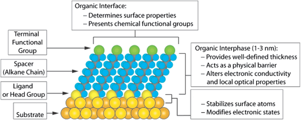
SAMs are themselves nanostructures with a number of useful properties. The thickness of a SAM is typically 1–3 nm, and SAMs are the most elementary form of a nanometer-scale organic thin-film material. The composition of the molecular components of the SAM determines the atomic composition of the SAM perpendicular to the surface. This characteristic makes it possible to use organic synthesis to tailor organic and organometallic structures at the surface with positional control approach. In this context, the SAMs could provide a convenient, flexible, and simple system to tailor the interfacial properties of metals, metal oxides, and semiconductors. Thereafter, the application of SAMs is a fantastic strategy to engineer the surface properties in perovskite solar cells and had attracted intensive focus within the most recent years. The fundamentals on SAMs e.g., definition, preparation, formation, structure, and applications, have been well reviewed in the literature. Reference Love, Estroff, Kriebel, Nuzzo and Whitesides40,Reference Ulman41,Reference Vericat, Vela, Benitez, Carro and Salvarezza56 Here, we will focus on the SAMs applied in perovskite solar cells. Basically, SAMs are organic assemblies formed by the adsorption of molecular constituents from solution or the gas phase onto the surface of solids. Illustration on functionality and characteristic of each component of SAMs is described in Fig. 1. These adsorbates might organize spontaneously into crystalline, semi-crystalline, or amorphous structures depending on the texture of the substrates and processing. The molecules that form SAMs should have a chemical functionality, or “headgroup”, with a specific affinity, e.g., covalent bonding to a substrate. There are a number of headgroups that can bind to specific metals, metal oxides, and semiconductors, such as thiols, carbonyl acid, phosphoric acid, silanes, etc. By control of the processing conditions and interactions between SAMs and substrates, the coverage ratio of SAMs on top of substrate surfaces can be controlled. Among all the parameters, the reactivity between the substrates and the headgroups of the SAMs is important for surface coverage ratio of SAMs. The terminal groups of SAMs determined the substrate surface properties including the surface chemical groups, work functions, etc. In perovskite solar cells, the most frequently used terminal groups included amino, ammonium, thiols, pyridines, cyano groups, etc, which determined the dipole moments and the chemical interactions between the perovskite layer and interfacial layer. The spacer between the terminal and headgroup determines the geometry of the SAM molecules to the substrates, e.g., tilting angles. For application in perovskite solar cells, the linkages consisted of inactive aliphatic and photo-active conjugated benzene spacers, and these linkages can influence the charge transport at the interface.
Schematic diagram for SAMs. Reprinted with permission from Ref. Reference Love, Estroff, Kriebel, Nuzzo and Whitesides40. Copyright (2005) American Chemical Society.

III. SAMS APPLIED IN PEROVSKITE SOLAR CELLS
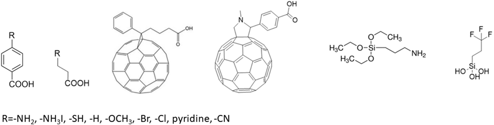
Different to the traditional SAMs (containing thiol headgroups) deposited on metals, the SAMs for perovskite solar cell application were target to anchor onto metal oxides (TiO2, ZnO, SnO2, NiO, etc.) or organic interlayers (PEDOT:PSS, etc.), which were most commonly used interfacial layers for perovskite solar cells. Reference Yang, Tao, Qin, Ke and Fang57–Reference Cho and Park59 And the terminal group was mainly designed to tune the work function of the interlayer for better energy level alignment with the perovskite layer, provide a miscible interface for smooth growth of the perovskite layer, and tailor the chemical interactions at the interfaces with the perovskite. Figure 2 depicts the SAMs used for perovskite solar cells. As can be seen, most of the SAMs feature carbonyl or silane functionalities as headgroup. Because the most common charge transporting layers were metal oxide layers, Reference Savva, Papadas, Tsikritzis, Armatas, Kennou and Choulis58 on top of which abundant hydroxyl group existed. And the interaction between the carbonyl group and metal oxide surface, e.g., chemical bonds or coordination of carbonyl group with metals, anchored the SAMs on top. Beyond the metal oxide layers, modification of PEDOT:PSS and carbonyl group rich surface with amino and silane was also reported by Gu et al. Reference Gu, Zuo, Larsen-Olsen, Ye, Wu, Krebs and Chen55 and Huang et al., Reference Bai, Dong, Shao, Deng, Wang, Shen, Wang, Wei and Huang60 respectively.
SAMs used in perovskite solar cells.

Besides the headgroup, the terminal group plays the most significant role in determining the perovskite solar cell performance. The current explored terminal groups include amino, Reference Zuo, Gu, Ye, Fu, Wu, Li and Chen31 ammonium chloride, Reference Ogomi, Morita, Tsukamoto, Saitho, Shen, Toyoda, Yoshino, Pandey, Ma and Hayase61 ammonium iodide, Reference Ogomi, Morita, Tsukamoto, Saitho, Shen, Toyoda, Yoshino, Pandey, Ma and Hayase61 thiol, Reference Cao, Yin, Yuan, Zhao, Li and Zheng54 hydrogen, Reference Wang, Chueh, Zhao, Cheng, Eslamian, Choy and Jen39 hydrocarbons, Reference Wang, Chueh, Zhao, Cheng, Eslamian, Choy and Jen39 benzene, pyridine, Reference Zuo, Chen, De Marco, Hsieh, Chen, Sun, Chang, Zhao, Dong and Yang33 bromo, chloro, fluoro, cyanide, C60, etc. Reference Zuo, Chen, De Marco, Hsieh, Chen, Sun, Chang, Zhao, Dong and Yang33,Reference Wang, Chueh, Zhao, Cheng, Eslamian, Choy and Jen39 These functional groups were designed with different purposes, which will be discussed in the following sections. It should be noted that the selection of SAMs should consider the effects they might have and the processing conditions. It should be noted that the species of SAMs applied in perovskite solar cells is quite limited. The progress on the design of novel SAMs for perovskite solar cells lagged behind that of the perovskite solar cells. This limited the broad application of SAMs in perovskite solar cells. Thereafter, a variety of functions with the novel SAMs are to be explored. The material and functionality limitation of SAMs for perovskite solar cells will be discussed in the following sections.
IV. DEPOSITION METHODS
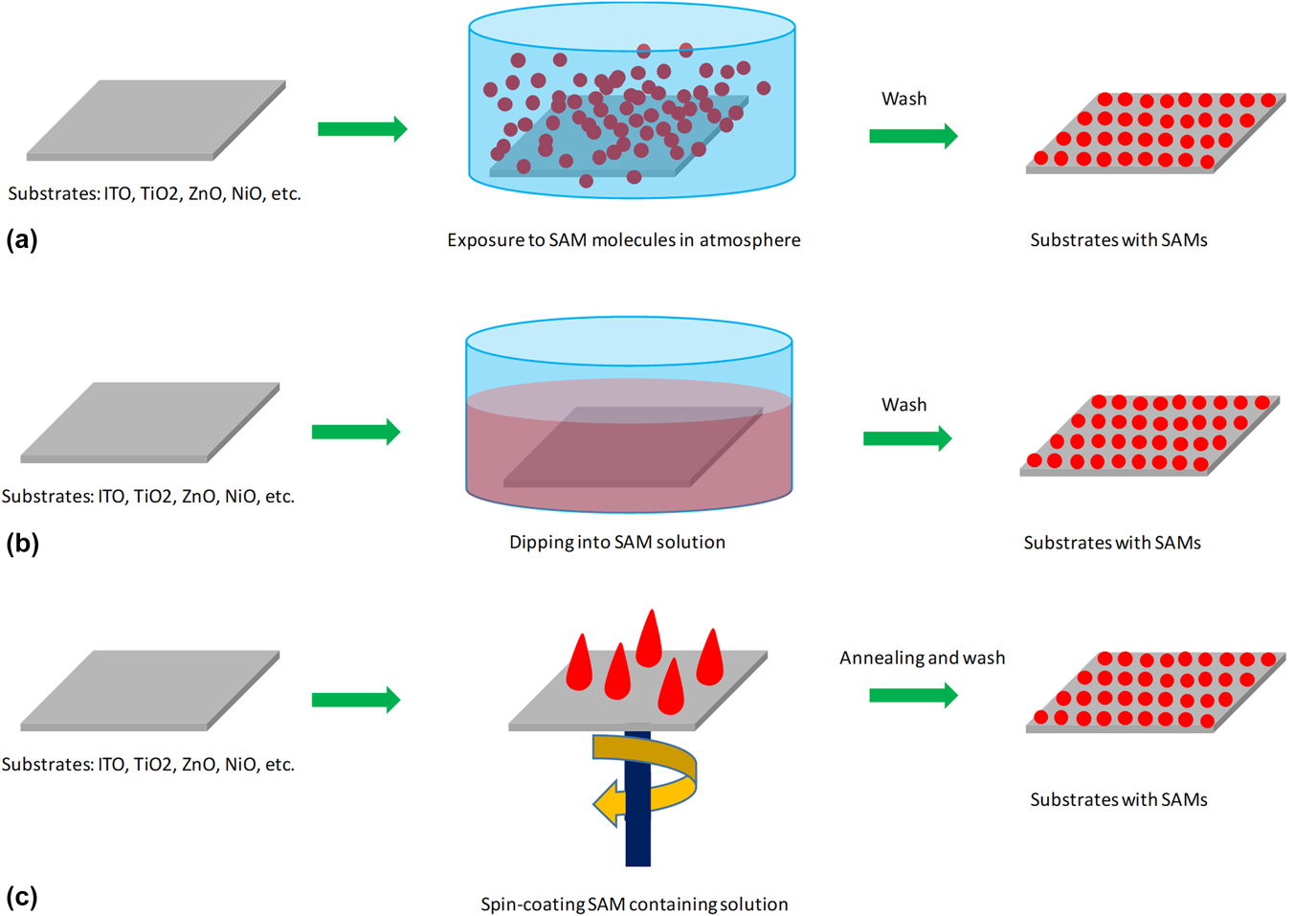
The SAMs can be deposited onto the substrates through a variety of methods. Reference Yan, Zharnikov, Gölzhäuser and Grunze62 Here, we summarized three mostly accessed strategies, i.e., vapor deposition, solution assisted self-assembly, and spin-coating method. The schematic diagram for each method was depicted in Fig. 3. For vapor deposition, the monolayer is formed by exposing a clean substrate to a SAM molecule-saturated atmosphere. Reference Dong, Wang, Ng and Mao63,Reference Deering, Van Lue and Kandel64 After the physical or chemical absorption, the substrates were thermally annealed to form stronger covalent bonds with SAMs, and excessive SAM molecules, which interact with substrates via weak bonds, i.e., van der Waals force, were washed away from the top surface to form a well-defined SAM modified substrate for further investigation or application. In case of vapor deposition, the chemicals of SAMs were mostly liquids that have appreciable saturated vapor pressure, e.g., octanethiol Reference Deering, Van Lue and Kandel64 and octadecyltrichlorosilane. Reference Bai, Dong, Shao, Deng, Wang, Shen, Wang, Wei and Huang60,Reference Dong, Wang, Ng and Mao63 Most of the SAMs, including deposition of dyes in dye-sensitized solar cells, were deposited through the solution-assisted self-assembly process [Fig. 3(b)]. Reference Hagfeldt, Boschloo, Sun, Kloo and Pettersson65–Reference Crudden, Horton, Ebralidze, Zenkina, McLean, Drevniok, She, Kraatz, Mosey, Seki, Keske, Leake, Rousina-Webb and Wu69 The substrates were immersed into the SAM molecule solutions for a while, and after absorbing the molecules, the substrates were lift up from the solution. Finally, the excessive SAMs were removed by washing with a good solvent to obtain the SAM molecules for further use. The SAM molecules used here are mostly solid or liquid with appreciable solubility in a good solvent. Concentration of the SAMs is usually 0.1–10 mM. This method is mostly adopted to modify the surface of mesoporous scaffold surfaces, e.g., TiO2. For the spin-coating method [Fig. 3(c)], the solution containing SAM molecules was spin-coated onto the top surface of substrate. After spun dry, the substrates were transferred to a hot plate with fixed temperature for a while. With the substrates cooling to room temperature, excessive SAM molecules were washed away with their good solvents. This method is mostly applied to planar heterojunction perovskite configurations. Reference Zuo, Dong, De Marco, Hsieh, Bae, Sun and Yang16,Reference Zuo, Gu, Ye, Fu, Wu, Li and Chen31,Reference Zuo, Chen, De Marco, Hsieh, Chen, Sun, Chang, Zhao, Dong and Yang33
Deposition methods for SAMs: (a) vapor deposition, (b) solution assisted self-assembly process, and (c) spin-coating method.

For application in perovskite solar cells, all the three deposition methods are involved. In most cases, the arrangement of SAMs on top of the substrate is not as ordered as that on the metals, owing to the rough surface of the charge transporting layer used in perovskite solar cells. However, the disordered SAM arrangement does not seem to influence its effect on perovskite solar cell performance. But, the coverage ratio of SAMs on top of the surfaces is an important parameter that directly influences the surface properties.
V. IMPROVED DEVICE PERFORMANCE WITH SAM DEPOSITION
With SAMs, general improvement in device performance was observed for perovskite solar cells, which are summarized in Table I. The effects of SAMs on device performance of perovskite solar cells will be discussed with different device architectures, namely the mesoporous TiO2-based device and the planar heterojunction device.
Summarized effect of SAMs on perovskite device performance.

A. SAMs for perovskite solar cells with mesoporous TiO2 scaffolds
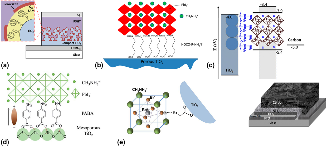
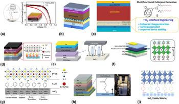
The broad application of mesoporous TiO2 in perovskite solar cells descended from dye-sensitized solar cells. And the mesoporous TiO2-based perovskite solar cells show several advantages, such as improving the electron extraction due to increased contact area, better long-term stability owing to stronger bondage at interfaces, Reference Wei, Ji, Song, Li, Cui, Li, Mbengue, Zhou, Ning and Park70 less hysteresis, etc. However, due to the high density of trap states, imperfect energy alignment with the perovskite, and low conductivity, the mesoporous TiO2 was mostly modified to guarantee enhanced electronic properties for high device performance. The first application of SAMs in perovskite solar cells was demonstrated by Snaith et al. (2013), Reference Abrusci, Stranks, Docampo, Yip, Jen and Snaith50 and the C60-based SAM molecules, which were developed by Jen et al Reference Hau, Cheng, Yip, Zhang, Ma and Jen71 for organic solar cells, were anchored to mesoporous TiO2 as a barrier layer [Fig. 4(a)]. It should be noted that the device structure at that stage was perovskite-sensitized type, where a thin layer of perovskite was attached on TiO2 and functioned mainly as the light absorber. Depositing C60-SAM was aimed to produce a dual absorbing, perovskite–polymer hole conductor hybrid solar cell, where the P3HT hole conductor also contributed to photocurrent due to the fast charge transfer between P3HT and C60-SAM. Unexpected improvement in V OC and fill factor (FF) was observed with C60-SAM, and they attributed it to the blocked electron transfer from perovskite to TiO2 and enhanced electronic coupling. The device with C60-SAM deposition shows significant improvement from 4% to 6.7% and from 10.2% to 11.7% with P3HT and Spiro-OMeTAD hole conductors, respectively.
Application of SAMs for perovskite solar cells with mesoporous TiO2 scaffolds. (a) C60-SAM, reprinted with permission from Ref. Reference Abrusci, Stranks, Docampo, Yip, Jen and Snaith50. Copyright (2013) American Chemical Society. (b) HI salt of glycine, beta-alanine and gama-aminobuteric acid. Reprinted with permission from Ref. Reference Ogomi, Morita, Tsukamoto, Saitho, Shen, Toyoda, Yoshino, Pandey, Ma and Hayase61. Copyright (2014) American Chemical Society. (c) Amino-propyltrimethoxysilane. Reprinted with permission from Ref. Reference Liu, Mei, Liu, Jiang, Sheng, Zhang and Han52. Copyright (2015) American Chemical Society. (d) 4-Aminobenzoic acid. Reprinted with permission from Ref. Reference Li, Chen, Liang, Gao and Huang51. Copyright (2015) the Royal Society of Chemistry. (e) BAA with MAPbBr3 perovskite. Reprinted with permission from Ref. Reference Kim, Im, Yoon, Sung, Kim, Kim and Lee53. Copyright (2015) the Royal Society of Chemistry.

Later, Ogomi et al. Reference Ogomi, Morita, Tsukamoto, Saitho, Shen, Toyoda, Yoshino, Pandey, Ma and Hayase61 demonstrated that the HI salt of glycine, beta-alanine, and gama-aminobuteric acid can significantly improve the perovskite solar cell performance [Fig. 4(b)]. With transient absorption (TA) and X-ray diffraction measurements, they conclude that the improved device performance with SAM deposition can be possibly attributed to a variety of factors including passivation of surface trap of porous titania layers, better growth of perovskite networks on porous materials, crystal growth of perovskite materials with uniform crystal plain, large crystal growth on porous materials, retardation of charge recombination by alkyl groups, and promotion of electron injection into titania. Shortly, Han et al. introduced the concept of SAM to fully printable perovskite solar cell with carbon electrodes, which showed great potential for practical application [Fig. 4(c)]. Reference Liu, Mei, Liu, Jiang, Sheng, Zhang and Han52 In their work, a silane-based SAM (amino-propyltrimethoxysilane) was deposited onto mesoporous TiO2 and improved the device performance from 9.7 to 11.7%. Moreover, the device shows improved stability with the silane SAM due to the more stable interfacial contact between the perovskite and TiO2. The successful application of SAMs in the potential industrialization device configuration suggested their application for further commercialization of perovskite solar cells. By replacing the alkane chain with photo-active bridge, Li et al. Reference Li, Chen, Liang, Gao and Huang51 adopted a benzene ring-bridged SAM (4-aminobenzoic acid) to modify the surface properties of mesoporous TiO2 and improved the device performance from 9.6 to 10.6% [Fig. 4(d)]. One of the most important features with perovskite solar cells is their tunable optoelectronic properties with different compositions. Extending the application of SAM to perovskite materials beyond the sophisticated MAPbI3 systems, Kim et al. Reference Kim, Im, Yoon, Sung, Kim, Kim and Lee53 studied the role of SAMs in MAPbBr3 systems [Fig. 4(e)]. A series of molecular carboxylates SAMs, including formic acid, deoxycholic acid, phthalic acid, acetic acid, and bromoacetic acid (BAA), were used to modify the mesoporous TiO2 surface. Among them, BAA showed the best effect and successfully improved the device performance from 2.6 to 5.6%. Further study using time-resolved photoluminescence measurements revealed that the presence of the interfacial carboxylate groups expedites electron injection from MAPbBr3 to TiO2. And the results from the pulsed light-induced transient measurements of photocurrent analysis showed that the lifetime of photo-injected electrons in the TiO2 CB was significantly increased with the passivation of the interface, implying the suppression of charge recombination as well.
B. SAMs for planar heterojunction perovskite solar cells
Over the mesoporous TiO2-based perovskite solar cells, the planar heterojunction solar cells feature simplified device architecture and low temperature processing. Together with rapid evolution in device performance (efficiency and stability), planar heterojunction perovskite solar cells show promising future commercialization. In planar heterojunction solar cells, even the polarity can be determined by the charge transporting layer, and thus, interfacial modifications were essentially important. The first application of SAM in planar heterojunction perovskite solar cells was introduced by Snaith [Fig. 5(a)]. Reference Wojciechowski, Stranks, Abate, Sadoughi, Sadhanala, Kopidakis, Rumbles, Li, Friend, Jen and Snaith72 They deposited C60-SAM onto a compact TiO2 surface and observed improved device performance. Moreover, the hysteresis problem was significantly suppressed with C60-SAM. With a systematic study on carrier dynamics by means of TA, transient photoluminescence, and capacitance–voltage, it was revealed that C60-SAMs can effectively improved the charge electron transfer from the perovskite to the TiO2 in the standard planar junction cells. An et al. Reference An, Fassl, Hofstetter, Becker-Koch, Bausch, Hopkinson and Vaynzof73 adopted another fullerene derivative (PCBA) as the interfacial layer for application in planar heterojunction solar cells with ZnO as the ETL [Fig. 5(b)]. They found that modification of the ZnO surface with PCBA results in a drastic improvement of the photovoltaic performance to the maximum value of 18% by nearly 100% compared with that without PCBA. Furthermore, Li et al. Reference Li, Zhao, Chen, Yang, Liu, Hong, Liu, Hsieh, Meng, Li and Yang74 synthesized a novel fullerene-based SAM (PCBB-2CN-2C8) with multifunctionalities, which improved the device performance by 20% [Fig. 5(c)]. In-depth analysis suggested that the PCBB-2CN-2C8 passivates the TiO2 surface and thus reduces charge recombination loss caused by the deep trap states of TiO2. Zuo et al. Reference Zuo, Gu, Ye, Fu, Wu, Li and Chen31 introduced SAMs with a much simpler structure to planar heterojunction perovskite solar cells, where a sol–gel processed ZnO layer was used as the ETL [Fig. 5(d)]. On top of ZnO, a monolayer beta-alanine was grown to reduce the work function of the ETL, passivate the trap states on ZnO, and provide a miscible interface for smooth growth of the perovskite layer. As a result, the averaged device performance significantly improved from 9.8 to 14.3%. Most recently, Azmi synthesized a novel SAM molecule to modify ZnO, which show superior performance in reducing the work function and morphology control, and thus efficiency was further improved to 18.8%. Reference Azmi, Hadmojo, Sinaga, Lee, Yoon, Jung and Jang75 On the surface of SnO2, Yang et al. Reference Yang, Wang, Lei, Zheng, Qin, Xiong, Zhao, Yan and Fang76 deposited a silane-based SAM (aminopropyltrimethoxysilane), which significantly improved the device performance to 18% [Fig. 5(e)]. As can be seen, most of the SAMs for perovskite solar cells feature the C60 and amino or the ammonium (the amino group could also change to ammonium group by grabbing HI from the perovskite precursors, e.g., methyammonium iodide) functionalities as terminal groups, which can effectively modified the surface of the ETL for improved device performance. To extend the varieties of terminal groups, Cao et al. Reference Cao, Yin, Yuan, Zhao, Li and Zheng54 explored the effect of SAMs with –SH as the terminal group for perovskite solar cells [Fig. 5(f)]. And they found that 4-mercaptobenzoic acid deposited on mesoporous TiO2 could facilitate electron transfer from perovskite to TiO2 and also alters the morphology of perovskite crystal growth to increase the device performance from 11.6 to 12.4%. Furthermore, SAMs of different terminal groups including benzene, amino, cyanine, and pyridine were systematically studied by Zuo et al. Reference Zuo, Chen, De Marco, Hsieh, Chen, Sun, Chang, Zhao, Dong and Yang33 in perovskite solar cells with SnO2 as the ETL [Fig. 5(g)]. With different SAMs, the interactions between ETL and perovskite can be tuned, e.g., the van der Waals type and coordination of different strength. The chemical interactions were also suggested to influence the interfacial optoelectronic properties and the subsequent device performance. It was observed that the pyridine group can form the most favorable interaction with perovskite due to surface passivation.
Application of SAMs in planar heterojunction solar cell. (a) C60-SAM. Reprinted with permission from Ref. Reference Wojciechowski, Stranks, Abate, Sadoughi, Sadhanala, Kopidakis, Rumbles, Li, Friend, Jen and Snaith72. Copyright (2014) American Chemical Society. (b) PCBA SAM, reprinted with permission from Ref. Reference An, Fassl, Hofstetter, Becker-Koch, Bausch, Hopkinson and Vaynzof73. Copyright (2014) Elsevier. (c) Fullerene SAM with multifunctional groups. Reprinted with permission from Ref. Reference Li, Zhao, Chen, Yang, Liu, Hong, Liu, Hsieh, Meng, Li and Yang74. Copyright (2015) American Chemical Society. (d) Beta-alanine. Reprinted with permission from Ref. Reference Zuo, Gu, Ye, Fu, Wu, Li and Chen31. Copyright (2015) American Chemical Society. (e) Silane SAM. Reprinted with permission from Ref. Reference Yang, Wang, Lei, Zheng, Qin, Xiong, Zhao, Yan and Fang76. Copyright (2016) the Royal Society of Chemistry. (f) SAMs with –SH as the terminal group. Reprinted with permission from Ref. Reference Cao, Yin, Yuan, Zhao, Li and Zheng54. Copyright (2015) the Royal Society of Chemistry. (g) Benzoic acid, 4-pyridine carboxylic acid, 4-cyano-benzoic acid, 4-aminobenzoic acid, and beta-alanine. Reprinted with permission from Ref. Reference Zuo, Chen, De Marco, Hsieh, Chen, Sun, Chang, Zhao, Dong and Yang33. Copyright (2016) American Chemical Society. (h) Beta-alanine in the inverted device. Reprinted with permission from Ref. Reference Gu, Zuo, Larsen-Olsen, Ye, Wu, Krebs and Chen55. Copyright (2015) the Royal Society of Chemistry. (i) 4-Aminobenzoic acid, 4-methoxybenzoic acid, benzoic acid, 4-chlorobenzoic acid, and 4-bromobenzoic acid. Reprinted with permission from Ref. Reference Wang, Chueh, Zhao, Cheng, Eslamian, Choy and Jen39. Copyright (2017) Wiley.

Among the planar heterojunction perovskite solar cells, the inverted structure, where ITO was modified as the anode, is also an important device configuration. Especially with the PCBM electron conductor, the hysteresis problem for inverted planar heterojunction perovskite solar cell could be eliminated. Gu et al. Reference Gu, Zuo, Larsen-Olsen, Ye, Wu, Krebs and Chen55 first introduced SAM to an inverted planar heterojunction perovskite solar cell, where the classic HTL poly(3,4-ethylenedioxythiophene) polystyrene (PEDOT:PSS) were modified by beta-alanine [Fig. 5(h)]. Different to the case of conventional devices, the amino group on beta-alanine was designed as headgroup to form ionic interaction with sulfonic acid on the PEDOT:PSS, and the carbonyl terminal group was supposed to provide a miscible surface for growth of perovskite solar cells. Due to the increased work function and improved perovskite morphology, significant improvement in device performance was observed from 9.7 to 11.6. Moreover, they show that SAMs was even more important for large area manufacturing using the roll-to-roll process, where the formation of the perovskite film was supposed to be different from the spin-coating process. Most recently, Qi et al. Reference Wang, Chueh, Zhao, Cheng, Eslamian, Choy and Jen39 conducted a systematic study on the role of SAMs for inverted perovskite devices with NiO as the interfacial layer [Fig. 5(i)]. By changing the electron affinity of the terminal groups, SAMs with different dipole moments were adopted. It was interesting to observe that the V OC of the perovskite devices monotonously changes with the dipole moment of the SAMs. Finally, dramatic improvement in device performance from 15.5 to 18.4% was achieved with 4-bromobenzoic acid.
C. SAMs on top of perovskite layers
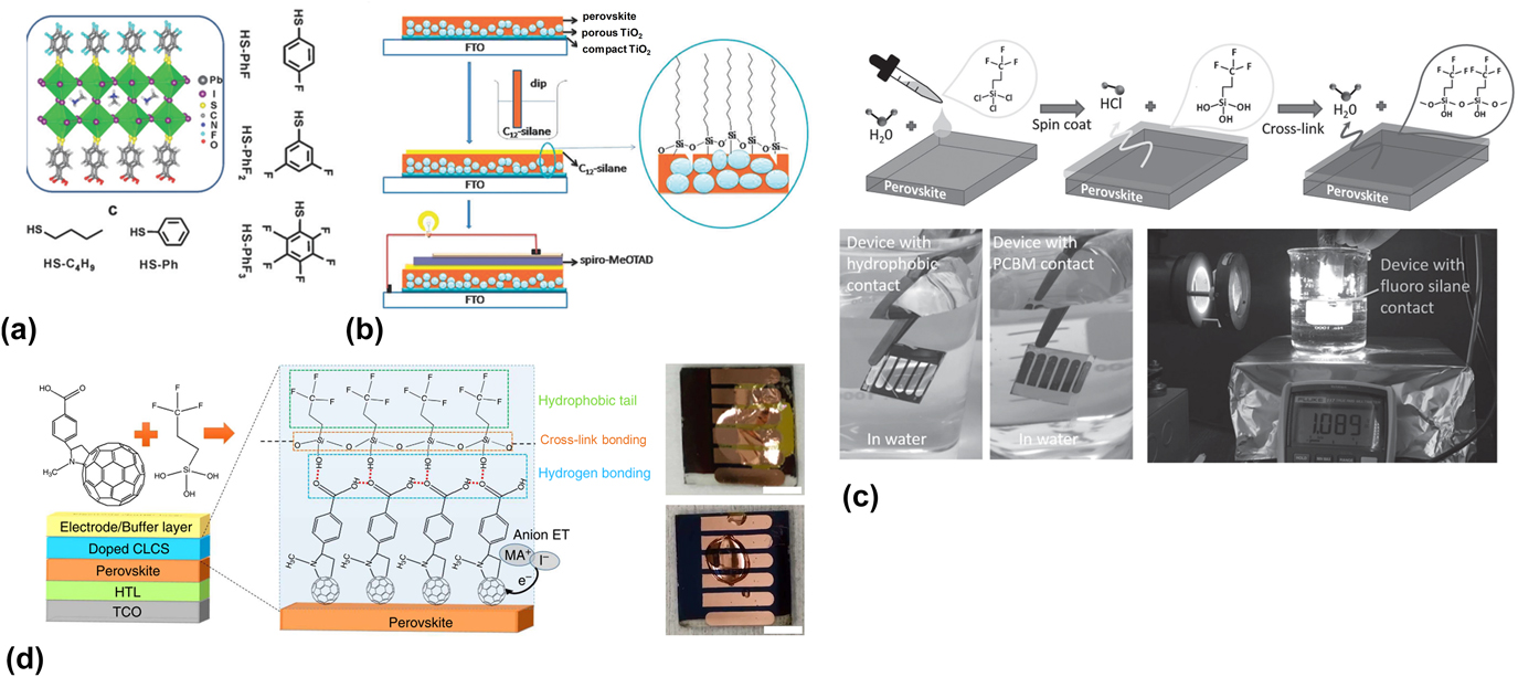
It should be noted that the ionic nature and existence of Pb2+ made the perovskite layer easily to form different chemical interactions with different functional groups and enable the possibility to modify the top surface of the perovskite layer for improving device performance and stability. Reference Zuo, Guo, deQuilettes, Jariwala, De Marco, Dong, DeBlock, Ginger, Dunn, Wang and Yang77 Thereafter, a variety of studies on the top layer modification were carried out (Fig. 6). Cao et al. Reference Cao, Yin, Yuan, Zhao, Li and Zheng54 modified the top surface of the perovskite layer with pentafluorobenzenethiol. The headgroup of thiol functionality can form firm coordination with the perovskite layer by coordination between the S-Pb, and the terminal group of pentafluorobenzene provides an ultra-hydrophobic surface to prevent the moisture from the perovskite solar cells [Fig. 6(a)]. Thereafter, improved device stability was achieved against moisture. Simultaneously, Zhang et al. Reference Zhang, Hu, Huang, Yue, Liu, Lu, Hu, Shang, Han and Zhu78 utilized dodecyltrimethoxysilane (C12-silane) to modify the top surface of the perovskite layer. C12-silane can be adsorbed onto the surface of the perovskite by hydrogen bonding of Si–OH with I−, leaving the long alkyl chain end group to stick out from the surface [Fig. 6(b)]. By properly choosing the concentration of C12-silane in isopropanol, a self-assembled monolayer can be formed. It was revealed that the C12-silane can form an electrically insulating barrier with the long alkyl chain and reduce interfacial charge recombination losses in perovskite solar cells and simultaneously change the hydrophilic nature of the perovskite surface to a hydrophobic one to endow the device with a higher resistance toward moisture. Most strikingly, Wang et al. Reference Wang, Dong, Li, Gruverman and Huang79 demonstrated perovskite solar cells that can work under water by forming a hydrophobic crosslinking layer with fluorinated silane SAM [Trichloro(3,3,3-trifluoropropyl)silane] [Fig. 6(b)]. The fluorosilane SAM simultaneously enhanced the device performance to 20% and improved the device stability against water. At the same time, Bai et al. Reference Bai, Dong, Shao, Deng, Wang, Shen, Wang, Wei and Huang60 bonded the crosslinkable silane SAM [Trichloro(3,3,3-trifluoropropyl)silane] on top of a fullerene-based ETL to make it highly water resistant [Fig. 6(b)]. With a crosslinkable silane-functionalized fullerene electron transport layer, the perovskite devices deliver an efficiency of 19.5% with a high FF of 80.6%. A crosslinked silane-modified fullerene layer also enhances the water and moisture stability of the nonsealed perovskite devices by retaining nearly 90% of their original efficiencies after 30 days’ exposure in an ambient environment.
SAMs on top of perovskite solar cells. (a) Pentafluorobenzenethiol, reprinted with permission from Ref. Reference Cao, Yin, Yuan, Zhao, Li and Zheng54. Copyright (2015) the Royal Society of Chemistry. (b) Dodecyltrimethoxysilane. Reprinted with permission from Ref. Reference Zhang, Hu, Huang, Yue, Liu, Lu, Hu, Shang, Han and Zhu78. Copyright (2015) the Royal Society of Chemistry. (c) Trichloro(3,3,3-trifluoropropyl)silane on perovskite layer. Reprinted with permission from Ref. Reference Wang, Dong, Li, Gruverman and Huang79. Copyright (2016) Wiley. (d) Tri-chloro(3,3,3-trifluoropropyl)silane on fullerene derivatives, reprinted with permission from Ref. Reference Bai, Dong, Shao, Deng, Wang, Shen, Wang, Wei and Huang60. Copyright (2016).

VI. MECHANISMS WITH IMPROVED EFFICIENCY AND STABILITY
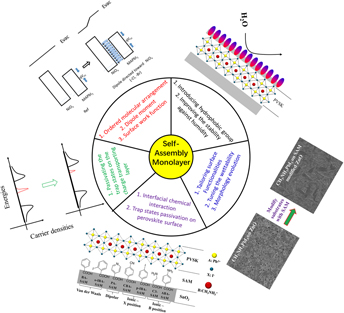
As proved, the application of SAMs is an effective strategy for improving the device efficiency, and the improvement in device performance can be originated from multiple reasons (Fig. 7).
Mechanisms with improved device performance of perovskite solar cells with SAM deposition.

First, the SAMs on the substrate surface can form ordered structure with well-defined unique orientation. The alignment of SAM molecules with one direction produces permanent dipole moment, which can effectively influence the surface work function of the charge transporting layer and the energy level alignment at the interface. Thereafter, through controlling the SAM species and their occupancy on the substrates, the surface work function can be controlled, and so it is with the interfacial optoelectronic properties and the device performance of perovskite solar cells. Generally, molecules with dipole moment directed from substrate to perovskite can be favorable for the ETL and vice versa for the HTL. The change of energy level alignment can influence the charge extraction and recombination at the interfaces, and the built-in potential could be increased with the SAMs. These results will affect the V OC, FF, and J SC. The most exemplary work was conducted by Wang et al., Reference Wang, Chueh, Zhao, Cheng, Eslamian, Choy and Jen39 where SAMs of different dipole moments were used.
Second, the SAMs can passivate the trap states on the charge transporting layer. The top surface of metal oxides are rich in dangling bonds or hydrogen, hydroxyl, carbonyl groups, and they might introduce deep trap states, which would increase charge recombination velocity at the surface. With deposition of SAMs, the dangling bonds or other chemical groups can be saturated or changed, which results in the trap passivation. The trap state passivation at the charge transporting layer surface will result in improved charge extraction efficiency and increase the FF. A systematic study on trap state passivation was carried out by Li et al. Reference Li, Zhao, Chen, Yang, Liu, Hong, Liu, Hsieh, Meng, Li and Yang74
Third, the SAMs can passivate the trap states in the perovskite layer. With different terminal groups, different chemical interactions, such as weak van der Waals force, ionic bond, and coordination bonds of different types, can be formed. It has been demonstrated both theoretically and experimentally that the terminations of perovskite crystals can influence the optoelectronic properties of the perovskite films deeply. And proper control of the chemical environments at the surface or grain boundaries can improve the device performance. Also, the interfacial chemical interaction between the perovskite layer and charge transporting layer can influence the electronic coupling between them. A systematic and independent study on the chemical interactions between the perovskite and ETL can be found in the literature by Zuo et al. Reference Zuo, Chen, De Marco, Hsieh, Chen, Sun, Chang, Zhao, Dong and Yang33
Fourth, the SAMs can influence the morphology of perovskite solar cells, Reference Aizenberg, Black and Whitesides32 especially for those formed via one-step solution process. Deposition of SAMs can provide a more miscible interface to induce a homogeneous film with less pin-holes caused by dewetting. On the other hand, it has been observed that the crystallization of perovskites from one-step method is dominated by the growth process, which means the crystal size is controlled by the seeding. It has been revealed that the seeding of the perovskite layer was controlled by the status of the perovskite precursor in solution and the substrate wetting properties. It is generally observed that the miscible interface facilitates large grain size of the perovskite film. Reference Zuo, Gu, Ye, Fu, Wu, Li and Chen31
Fifth, SAMs could retard charge recombination with insulating barrier. SAMs formed an insulating barrier between the perovskite layer and the charge transporting layer, which might prevent charge recombination similar to the heterojunction with the intrinsic thin-layer (HIT) solar cell. Reference Zhang, Hu, Huang, Yue, Liu, Lu, Hu, Shang, Han and Zhu78,Reference Wang, Dong, Li, Gruverman and Huang79
On the other hand, the stability of perovskite solar cells, especially for the stability against moisture, can be greatly improved with SAMs mainly due to the incorporation of super hydrophobic groups, e.g., fluoro, to prevent the humidity from permeating. Reference Bai, Dong, Shao, Deng, Wang, Shen, Wang, Wei and Huang60 Also, alteration of chemical bonds at the surface of the perovskite can help against water deterioration. Reference Zuo, Guo, deQuilettes, Jariwala, De Marco, Dong, DeBlock, Ginger, Dunn, Wang and Yang77
VII. CURRENT LIMITATIONS AND FUTURE LANDSCAPES
As can be seen, the advantages of SAMs lie on their ease of processing, effectiveness for versatile purposes, and compatibility with large area manufacturing. However, it is clear that the species of SAMs specifically designed for perovskite solar cells is quite limited. Currently, most of the SAM species used in perovskite solar cells were commercially purchased, and each of the functional groups, e.g., terminal, head, and spacer groups, were selected based on the availability. Thereafter, no specific SAM species had been demonstrated targeting the perovskite solar cell application. And except the fullerene derivatives, most of the SAMs were small molecules with very simple molecular structure. For further improving the device performance with SAMs, novel SAM species were severely required to fulfill specific purposes, and this expectation is validated by Azmi et al., where novel SAM molecules were specially designed and further improved efficiency was achieved. Reference Azmi, Hadmojo, Sinaga, Lee, Yoon, Jung and Jang75 Nevertheless, more terminal groups can be designed to explore better interactions for smooth growth of perovskite films and surface passivation. Diverse linkages can be proposed to study the effect of SAM geometries on device performance, investigate the tunneling effect at molecular level (e.g., distance control and effect of linkage species), and provide insight into insulating barrier effect on the carrier dynamics. Versatilities of headgroups can be explored to achieve optimal passivation on the perovskite layer interfaces. Design of different terminal groups to control the chemical environment or the charge densities at the perovskite surfaces can help to understand the mechanisms of grain boundary and interfacial passivation mechanism and generate profound impact for further developing high device performance perovskite solar cells. Since the SAMs can fulfill different purposes for perovskite solar cells, it would be interesting to explore whether synergistic effects will occur by simultaneously applying several different SAMs on one single substrate for better device performance. This efficacy of this strategy was recently demonstrated by Chen et al., Reference Chen, Cao, Wu, Jing, Wu and Zheng80 where they used SAM molecules, i.e., aminocaproic acid and caproic acid simultaneously to improve both of the stability and efficiency of perovskite solar cells.
Moreover, going beyond the thin SAM limitation, SAMs of super molecular structures can be designed via SAMs of large molecules or the layer-by-layer self-assembling process. Self-assembling of super molecular structures can potentially enable more interesting phenomenon and pronounced effect within perovskite solar cells. Furthermore, self-stratification occurs on the vertical distribution of gradient compositions when blending perovskite with other components, e.g., fluorinated fullerene derivative, and it is rational to use similar process to finish perovskite solar cell device fabrication with one time spin-coating, where the HTL, ETL, and perovskite layers can spontaneously stratify to form a sandwiched structure. This will greatly simplify the device fabrication, which is essentially important to reduce the manufacturing cost of perovskite solar cell commercialization. Also, templating effect of the SAMs for crystal growth of perovskite films can potentially enable epitaxial growth of the single crystal (or large crystal size) perovskite layer with few boundaries. Thereafter, with more efforts on the SAMs, more new and exciting things can be expected to boost the perovskite solar cells to a new level.
Another limitation lies on that the current achievement in improved device performance with SAM modification focused on amending the material flaws to make them work smoothly. Although the SAMs show advantages to resolve these issues for high device performance, similar effects can be reached via other techniques. For example, the passivation effect for the charge transporting layer with abundant trap states at the surface can also be achieved via delicate processing or post-treatment of charge transporting layers, morphology of the perovskite film can be controlled by advanced film deposition techniques, stability against moisture can be realized via hydrophobic interfacial layers or the design of 2D structures, and interfacial energy alignment can be tuned using the charge transporting layer of different work functions. To get out of the minor “position” and make the SAMs an indispensable component for perovskite solar cell application, a necessary step should be taken to replace the charge transporting layer with layers of SAMs to compose the perovskite device. To achieve this goal, novel SAMs should be designed by taking all of the factors within the charge transporting layer into considerations, e.g., the intrinsic work function, conductivity, chemical interaction, coverage ratio, and energy level alignment. We believe that this is available by tailoring the headgroup, spacers, and terminal groups within the SAMs, together with suitable processing, e.g., super molecular assembly technique, layer-by-layer deposition of different SAMs, and combination of different SAMs of multiple functions into one layer.
VIII. SUMMARY AND OUTLOOK
We summarized the recent development of SAMs for perovskite solar cells. With the tunable molecular structure for adaption in various circumstances, the SAMs show promising application for perovskite solar cells on a variety of device architectures for different perovskite systems. The mechanisms for improving device performance implied their versatility for application in perovskite solar cells for a variety of purpose, e.g., tuning work function of the charge transporting layer, trap state passivation, controlling perovskite film morphology, etc. Moreover, processing of SAMs can be easily fulfilled with large area manufacturing, e.g., the roll-to-roll process, due to their monolayer texture. Washing away the excessive SAMs without bonding the substrate spare the trouble for precise control in layer thickness, which is a great challenge for thin-film deposition. These features endow the SAMs with great potential to explore the device performance of perovskite solar cells and future manufacturing. However, the efforts on SAMs for perovskite solar cells is quite limited. Thereafter, more efforts should be put to explore the novel SAMs for perovskite applications.