Introduction
Most approaches to photon management in photovoltaics (PV) focus on increasing the total absorbed irradiance I abs from the incident solar irradiance I sun through some modification of the photovoltaic material. The total absorbed irradiance of a material, obtained from Beer’s law, is:

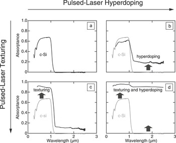
where R and α are the wavelength-dependent reflectance and absorption coefficients, respectively; d is the path length of a photon through the material; and the integration is over all optical wavelengths λ. Thus, neglecting wavelength conversion approaches, photon management requires manipulating one or more of three material parameters: α, R, or d. Pulsed-laser processing of semiconductors with nanosecond, picosecond, or femtosecond laser pulses offers two very different approaches to enhance photon absorption: pulsed-laser hyperdoping and surface texturing. For example, the “black silicon” process we have reviewed previously for the MRS Bulletin Reference Tull, Carey, Mazur, McDonald and Yalisove1 achieves near-unity, broadband absorption of visible and near infrared light in silicon with femtosecond laser processing. The effects of these techniques on light absorption are summarized in Figure 1.
Absorption enhancement from pulsed-laser hyperdoping and surface texturing. The absorptance A is obtained from the expression A = 1–R–T, where R and T are reflectance and transmittance, respectively, measured with an integrating sphere to collect both specular and diffuse light. (a) Untreated crystalline silicon (c-Si) has negligible absorption of light with a wavelength longer than 1.1 μm due to its energy bandgap. (b) Pulsed-laser hyperdoping with sulfur enables absorption of sub-bandgap light. (c) Pulsed-laser texturing enhances above-bandgap light absorption with geometric light trapping. (d) Broadband near-unity absorption is achieved with both pulsed-laser hyperdoping and surface texturing. Adapted from References Reference Winkler38 and Reference Crouch, Carey, Shen, Mazur and Genin39.

First, pulsed-laser irradiation can be used to introduce non-equilibrium concentrations of dopants into silicon, a process we refer to as hyperdoping. This process changes silicon’s electronic structure and increases the absorption coefficient α.Reference Wu, Crouch, Zhao, Carey, Younkin, Levinson, Mazur, Farrell, Gothoskar and Karger2–Reference Sheehy, Tull, Friend and Mazur5 Second, pulsed-laser irradiation of a silicon wafer can produce micrometer- or nanometer-scale surface textures that are suitable for geometric light trapping.Reference Crouch, Carey, Warrender, Aziz, Mazur and Genin6–Reference Iyengar, Nayak and Gupta8 Hyperdoping significantly increases the absorption coefficient through the inclusion of a high concentration of new electronic states. The process depends on the fast resolidification that follows pulsed-laser melting, which traps dopant atoms at concentrations far above equilibrium solubility limits.Reference White, Wilson, Appleton and Young9, Reference Reitano, Smith and Aziz10 Realizing such dopant concentrations with deep-level impurities is a possible route to fabricating an intermediate band photovoltaic cell, a high-efficiency PV concept.Reference Luque and Marti11 Surface texturing, on the other hand, increases the fraction of absorbed photons by increasing d and effectively decreasing R(λ) (Equation 1). Texturization relies on laser-induced ablation of silicon, which selectively removes material to create light trapping morphologies. These two pulsed-laser approaches to photon management are distinct and can be realized independently, although much research in this field has focused on a combination of these two effects.Reference Crouch, Carey, Warrender, Aziz, Mazur and Genin6, Reference Liu, Liu, Wang, Feng, Zhu and Zhao12–Reference Bassam, Parvin, Sajad, Moghimi and Coster14
In this article, we review pulsed-laser hyperdoping and surface texturing, summarize the current state of the art for both techniques, and discuss outstanding questions and challenges for each application. We first describe the basic physics of laser-induced melting, how it leads to hyperdoping and changes in the absorption coefficient, and ongoing research directions in this field toward realizing efficient photovoltaic devices. Next, we describe laser ablation and how it leads to surface geometries that are advantageous for geometric light trapping. Finally, we comment on current directions and possible near-term applications in this exciting field.
Hyperdoping
Pulsed lasers have been used in doping processes since the 1960s, including laser-assisted doping,Reference Affolter, Luthy and Vonallmen15, Reference Fairfiel and Schwuttk16 gas immersion laser doping,Reference Carey, Sigmon, Press and Fahlen17, Reference Carey, Bezjian, Sigmon, Gildea and Magee18 pulsed laser mixing,Reference Tabbal, Kim, Woolf, Shin and Aziz19 and laser-induced diffusion.Reference Fogarassy, Stuck, Grob and Siffert20 Lasers with pulse durations between hundreds of femtoseconds and tens of nanoseconds can achieve dopant concentrations that exceed the solid solubility limit by several orders of magnitude. Although we focus on silicon in this article, alternative laser-processes have been explored for other materials, including binaryReference Kim, Alberi, Dubon, Aziz and Narayanamurti21 and quaternaryReference Yu, Walukiewicz, Wu, Shan, Beeman, Scarpulla, Dubon and Becla22–Reference Yu, Walukiewicz, Ager, Bour, Farshchi, Dubon, Li, Sharp and Haller24 materials. The hyperdoping process can introduce dopant states that enhance absorption at photon energies above and below the bandgap, making it a potential route to realizing intermediate band photovoltaic devices.
Laser melting and doping
When a laser pulse delivers energy to a solid volume at a rate sufficiently in excess of any cooling processes, such as conduction to the underlying bulk, it can raise the solid’s temperature above the melting point and cause a layer near the surface to melt. Pulsed lasers are well-suited to this application for two reasons. First, for laser pulses that are nanoseconds or shorter in duration, the energy is deposited over a timescale that is comparable to or shorter than that of heat diffusionReference Sundaram and Mazur25—thus heat accumulates faster than it can be conducted away to the substrate. Second, because of their high spatial coherence, laser pulses can be focused to small areas, and the pulse energy is absorbed in a small volume. Laser pulses with durations in the range of 10−13−10−8 s have been used to achieve temperatures sufficient for melting a layer of silicon near the surface, typically 50–500 nm thick.Reference Lompre, Liu, Kurz and Bloembergen26–Reference Kittl, Sanders, Aziz, Brunco and Thompson28 Because this thin layer of laser-melted material is resting atop a room-temperature lattice, the heat flux away from the molten region is large, and the resolidification front moves quickly through the material, potentially exceeding 10 m/s.Reference White, Wilson, Appleton and Young9, Reference Liu, Yen, Bloembergen and Hodgson29 The standard Czochralski crystal growth process, in comparison, typically involves resolidification fronts with speeds of about 10−5 m/s.Reference Hull30
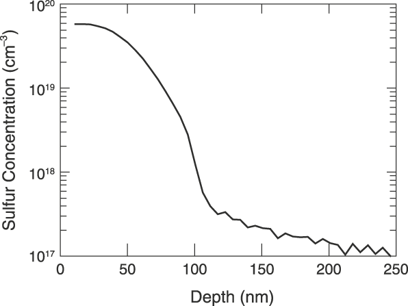
As the resolidification-front velocity approaches 1 m/s, thermodynamic equilibrium cannot be established at the liquid-solid interface.Reference White, Wilson, Appleton and Young9 As a result, dopant atoms present in the melt are trapped in the solid silicon above their equilibrium solubility limit, a process known as solute trapping.Reference White, Wilson, Appleton and Young9, Reference Reitano, Smith and Aziz10, Reference Emel’yanov and Babak31 According to well-tested predictive models, faster resolidification velocities yield higher dopant concentrations.Reference White, Wilson, Appleton and Young9, Reference Reitano, Smith and Aziz10, Reference Kittl, Sanders, Aziz, Brunco and Thompson28, Reference Aziz and White32 At sufficiently high resolidification velocities (>15 m/s), however, solute segregationReference Hoglund, Thompson and Aziz33 and loss of crystalline orderReference Thompson, Mayer, Cullis, Webber, Chew, Poate and Jacobson34 during resolidification occur. Figure 2 shows a sulfur concentration profile after fs-laser irradiation of silicon in a sulfur-rich atmosphere. The sulfur concentration approaches 10Reference Fogarassy, Stuck, Grob and Siffert20 cm−3 near the surface, about four orders of magnitude above the solid solubility limit.Reference Carlson, Hall and Pell35
Sulfur concentration obtained by secondary ion mass spectrometry after pulsed-laser hyperdoping with 800-nm fs-laser pulses in a SF6 atmosphere at a pressure of 6.7 × 10⁴ Pa. The sample is irradiated with a small number of laser pulses, and the surface is free of texture (roughness less than 3 nm). Sulfur concentration near the surface is 6 × 1019 cm−3, three orders of magnitude larger than the solubility limit of sulfur in silicon. Adapted from Reference Reference Winkler38.
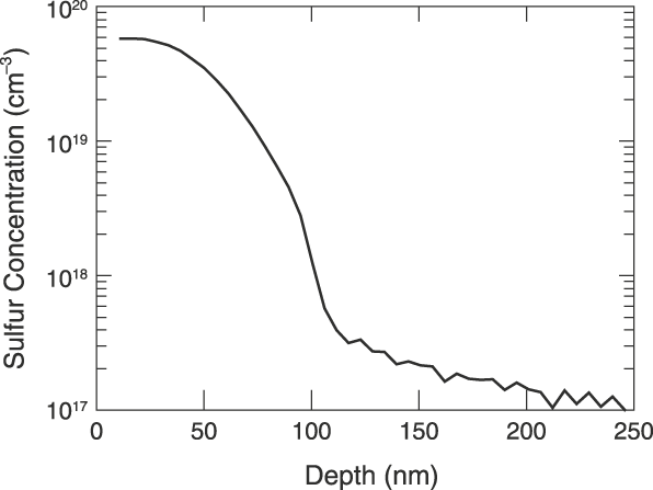
Dopants can be introduced into the host material via diffusion from a dopant-rich atmosphere while the substrate is molten. Introducing the dopants via ion implantation prior to laser melting is more common, however.Reference White, Wilson, Appleton and Young9 In the case of diffusion into molten silicon, the dopant precursor can be a gaseous ambient or a thin solid film on top of the silicon. Pulsed-laser hyperdoping of heavy chalcogen (S, Se, and Te) in silicon has been achieved via all of the methods mentioned previously using femtosecond,Reference Wu, Crouch, Zhao, Carey, Younkin, Levinson, Mazur, Farrell, Gothoskar and Karger2, Reference Crouch, Carey, Warrender, Aziz, Mazur and Genin6, Reference Zorba, Boukos, Zergioti and Fotakis13 picosecond,Reference Zorba, Boukos, Zergioti and Fotakis13 or nanosecondReference Kim, Warrender and Aziz3, Reference Bob, Kohno, Charnvanichborikarn, Warrender, Umezu, Tabbal, Williams and Aziz4, Reference Crouch, Carey, Warrender, Aziz, Mazur and Genin6, Reference Zorba, Boukos, Zergioti and Fotakis13, Reference Tabbal, Kim, Woolf, Shin and Aziz19 laser pulses.
The heat-transfer and resolidification processes described previously are common to laser-induced melting using pulses with durations of tens of nanoseconds and shorter. However, the duration of laser pulses used for hyperdoping ranges over five orders of magnitude, and significant differences occur across these timescales. For femtosecond pulses, laser energy is deposited into the material well before heat diffusion occurs. First, electrons absorb the energy of the laser pulse, and then this high-temperature electron gas transfers energy to the cold lattice through electron-phonon coupling on a picosecond timescale.Reference Sundaram and Mazur25 In addition, nonlinear absorption reduces the photon penetration depth, and the pulse energy is deposited in a very thin layer, lowering the energy threshold for melting.Reference Korfiatis, Thoma and Vardaxoglou36 In this case, the resolidification-front velocity can greatly exceed the liquid-to-crystal relaxation rate, yielding resolidification into an amorphous phase.Reference Thompson, Mayer, Cullis, Webber, Chew, Poate and Jacobson34, Reference Bonse, Baudach, Kruger, Kautek and Lenzner37 For nanosecond laser pulses, the absorption process is linear, and the absorption length is larger. Thus, deeper melt depths and dopant distributions can be achieved. The temperature gradient across the molten layer and the solid substrate is smaller than for a laser pulse of femtosecond duration, resulting in a longer melt duration and slower resolidification-front velocity. Therefore, ns-laser hyperdoped silicon is often crystalline, while fs-laser hyperdoped silicon often has an amorphous or polycrystalline structure.Reference Crouch, Carey, Warrender, Aziz, Mazur and Genin6, Reference Winkler38 To summarize, the duration of a laser-pulse determines the kinetics of melting and resolidification, and hence significantly impacts dopant incorporation and changes in crystal structure.
Hyperdoping with femtosecond lasers
We now discuss the “black silicon” process: hyperdoping silicon with heavy chalcogen atoms via irradiation with 100-fs, 800-nm Ti:sapphire laser pulses. The dopants are introduced via a chalcogen-rich ambient, such as gaseous sulfur hexafluoride (SF6) or a thin solid film of Se or Te (deposited on the silicon surface via thermal evaporation prior to laser irradiation). After fs-laser hyperdoping, the chalcogens are incorporated at concentrations of about 1 at.%Reference Sheehy, Tull, Friend and Mazur5, Reference Crouch, Carey, Shen, Mazur and Genin39—greater than the equilibrium solubilityReference Carlson, Hall and Pell35, Reference Vydyanath, Lorenzo and Kroger40, Reference Janzen, Grimmeiss, Lodding and Deline41 by a factor of 104. This process can be tuned to simultaneously produce a light-trapping surface texture (see next section) in addition to hyperdoping. We emphasize that with an appropriate choice of laser parameters, hyperdoping can be achieved without surface texturization.Reference Winkler38
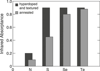
The optical absorptance of silicon hyperdoped with sulfur is shown in Figure 1b and 1d. In Figure 1b, the laser treatment was designed to avoid any surface texturization and shows that hyperdoping is responsible for the sub-bandgap absorption. In Figure 1d, absorptance is plotted for samples that have been both hyperdoped as well as textured. Combining hyperdoping and surface texturing, absorptance is near unity for both above and below bandgap light. The absorptance for silicon hyperdoped with Se and Te is nearly identical to that of silicon hyperdoped with S (shown in Figure 1d);Reference Sheehy, Tull, Friend and Mazur5Figure 3 shows the average infrared (IR) absorptance of optical wavelengths 1.25 to 2.5 μm for samples irradiated with and without chalcogen dopant precursors. Chalcogen-hyperdoped silicon exhibits broadband absorption extending to photon energies less than the bandgap of silicon. Three observations indicate that the high chalcogen concentration is responsible for this broadband, sub-bandgap absorption. First, we observe the broad sub-bandgap absorption if, and only if, a heavy chalcogen is present. We have experimented extensively with other dopantsReference Sheehy, Winston, Carey, Friend and Mazur42, Reference Younkin, Carey, Mazur, Levinson and Friend43 and phases of dopant precursors (solidReference Sheehy, Tull, Friend and Mazur5, Reference Tull, Winkler and Mazur44 versus gaseousReference Sheehy, Winston, Carey, Friend and Mazur42) and demonstrated that the presence of the chalcogen dopant is necessary and sufficient for strong sub-bandgap absorption. We show a selection of these data in Figure 3. Second, the sub-bandgap absorption decreases after thermal annealing in a manner directly related to the specific chalcogen-dopant used.Reference Crouch, Carey, Shen, Mazur and Genin39, Reference Tull, Winkler and Mazur44Figure 3 shows the average IR absorptance following a 30 min. anneal at 775 K for various dopants. The absorptance decreases at rates that are governed by the chalcogen-dopant diffusivity in silicon. For example, Te atoms have the lowest diffusivity among chalcogen atoms; consequently, the sub-bandgap absorptance of a Te-doped sample changes least after annealing. A chalcogen-dopant diffusion model explains the correlation between infrared absorption and the thermal treatment.Reference Tull, Winkler and Mazur44 Lastly, silicon hyperdoped with chalcogens using a different technique (ion implantation followed by nanosecond pulsed laser melting) exhibits similar sub-bandgap absorption.Reference Kim, Warrender and Aziz3, Reference Bob, Kohno, Charnvanichborikarn, Warrender, Umezu, Tabbal, Williams and Aziz4 Thus, regardless of the hyperdoping method, silicon hyperdoped with approximately 1 at.% of heavy chalcogens exhibits broadband absorption of photons with energy less than the bandgap of silicon.
Average infrared (λ = 1.25 to 2.5 μm) absorptance of chalcogen hyperdoped silicon before and after annealing (775 K, 30 min.), represented by dark and light gray bars respectively. Samples are irradiated in the presence of a sulfur dopant precursor (sulfur hexafluoride SF6 or hydrogen sulfide H2S) (S), selenium (Se), or tellurium (Te). After laser irradiation, these samples exhibit a surface roughness similar to that of Figure 4a. Before annealing, all chalcogen hyperdoped samples exhibit near unity sub-bandgap absorption. After annealing, the decrease in absorbtance is due to dopant diffusion. The absorptance of a sample irradiated without a chalcogen dopant precursor in a nitrogen (N) atmosphere is shown for comparison. Adapted from References Reference Sheehy, Tull, Friend and Mazur5 and Reference Tull, Winkler and Mazur44.

The origins of this absorption can be understood by considering the energy states of the chalcogens in silicon.Reference Janzen, Stedman, Grossmann and Grimmeiss45 Dilute concentrations of sulfur introduce a variety of occupied electronic states (arising from point defects, dimers, and more complex structures) that reside 100–300 meV below the conduction band edge of silicon; as a result, the sulfur dopants are electron donors.Reference Carey, Crouch, Shen and Mazur46 As the sulfur-concentration increases, new atomic configurations become likely, and these energy levels shift and broaden.Reference Thomas, Capizzi, Derosa, Bhatt and Rice47 Low energy photons can be absorbed by exciting electronic transitions between the band edges and the energy states introduced by sulfur. Thus, the presence of these states and the electronic transitions they facilitate are most likely responsible for the observed extended infrared absorption.
Finally, absorption of these sub-bandgap photons yields mobile charge carriers. Using sulfur as both an electron donor and as an optically sensitive defect, we have fabricated a variety of optoelectronic devices based on the junction formed between the substrate and the hyperdoped region.Reference Carey, Crouch, Shen and Mazur46, Reference Myers, Farrell, Karger, Carey and Mazur48, Reference Huang, Carey, Liu, Guo, Mazur and Campbell49 For example, we demonstrated photodiode devices that respond to sub-bandgap photons,Reference Carey, Crouch, Shen and Mazur46 with a measurable photoresponse at photon energies as low as 0.8 eV. Thus, it is unlikely that free-carrier absorptionReference Schroder, Thomas and Swartz50 and structural-defect absorptionReference Zanatta and Chambouleyron51 are responsible for this sub-bandgap absorption. Both of these effects enable absorption of sub-bandgap photons, but do not increase the population of mobile charge carriers, and therefore the absorbed energy cannot be extracted. In addition, the broad, featureless absorption shown in Figure 1b and 1d does not exhibit the predicted wavelength dependence of these effects.
Applications to photovoltaics
Next we consider the question of whether the strong sub-bandgap absorption of hyperdoped silicon can be used to increase photovoltaic efficiency. The idea of using dopants to increase absorption of low-energy photons (and thus increase PV cell efficiency) has a long history. The first proposal, suggested over 50 years ago, focused on using deep-level impurities to enhance absorption.Reference Wolf52 This concept, now further developed, is known as the impurity photovoltaic (IPV) effect.Reference Keevers and Green53 The principle of an IPV cell is to convert below-bandgap photon energy to electron-hole pairs through a two-stage, defect-assisted absorption process. However, deep electronic states are highly localized;Reference Landsberg54 their presence introduces localized pockets of charge that disrupts the local electrostatic potential in the silicon lattice and leads to increased non-radiative recombination rates.Reference Landsberg54 Thus, efforts to increase absorption through the inclusion of such states yield shorter carrier lifetimes and lower open-circuit voltage; consequently, cell efficiency can only be increased by 1–2% (absolute) using this method.Reference Keevers and Green53 On the other hand, it was recently pointed out that if such impurity states were included in high enough concentrations that their electronic states delocalize (through a Mott metal-insulator transition, for example), high recombination rates might be avoided.Reference Luque, Marti, Antolin and Tablero55 Such an intermediate band photovoltaic (IBPV) material could convert sub-bandgap photons to current without decreasing the open-circuit voltage in the cell, thus achieving a theoretical energy-conversion efficiency of >63%, significantly higher than the 41% efficiency limit of a standard single-junction solar cell.Reference Luque and Marti56, Reference Shockley and Queisser57 Fabricating an IBPV, however, is difficult, and no current design has demonstrated the theoretically predicted efficiency improvements.Reference Luque and Marti11
Pulsed-laser hyperdoping yields a material that exhibits several of the characteristics expected from an IBPV material. First, chalcogen-hyperdoped silicon exhibits strong photon absorption and measurable photoresponse for sub-bandgap light. Second, we have recently observed evidence that a metal-insulator transition occurs in silicon hyperdoped with chalcogens.Reference Winkler, Recht, Sher, Said, Mazur and Aziz58 As mentioned previously, such a delocalization transition is a necessary condition to avoid strong non-radiative recombination due to localized deep states. Silicon hyperdoped with titanium has demonstrated evidence of this lifetime recovery effect,Reference Antolin, Marti, Olea, Pastor, Gonzalez-Diaz, Martil and Luque59 but there are no reports yet of sub-bandgap absorption in that material. With both experimental and theoretical work devoted to investigating the mechanism and impact of intermediate band formation in hyperdoped silicon,Reference Winkler, Recht, Sher, Said, Mazur and Aziz58, Reference Newman, Sullivan, Winkler, Sher, Marcus, Fakra, Smith, Gradecak, Mazur and Buonassisi60, Reference Mo, Bazant and Kaxiras61 we are evaluating this material as a potential intermediate band system that could effectively capture the energy of sub-bandgap photons.
Surface texturization
Pulsed lasers are uniquely suited for hyperdoping because they heat small volumes of silicon over short timescales; for the same reason, they are also well-suited for creating surface texture. By providing highly localized heating, pulsed lasers can remove material through ablation to create surface texture. Their coherent properties lead to surface roughness with a characteristic length scale tunable by appropriate wavelength selection. We begin this section with a brief description of how pulsed-laser surface texturization occurs, and then explain its application to geometric light trapping in photovoltaics.
Pulsed-laser surface texturization
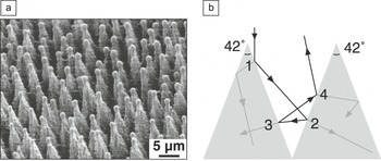
The physics of pulsed-laser texturization originates with the same processes described in the section on laser melting and doping. Because of interference between the incident laser pulse and self-scattering from surface defects, the energy deposited by a single laser pulse varies across the irradiated surface. This interference effect, which occurs over distances comparable to the incident laser wavelength, yields periodic variations in melt depth. Capillary waves, excited spontaneously in the melt, freeze in place during resolidification to form features known as laser-induced periodic surface structures (LIPSS). The periodicity of LIPSS is related to the wavelength and polarization of the incident light.Reference Sipe, Young, Preston and Vandriel62–Reference Young, Sipe and Vandriel64 Subsequent laser pulses are thus incident on a modulated surface and focus preferentially into the “valleys” of these features. If the energy deposited in these valleys is sufficient to raise the temperature above the boiling point, the molten silicon becomes superheated and begins to boil. Additional increases in energy can lead to a significant increase in the rate of material removal, a process known as ablation.Reference Cavalleri, Sokolowski-Tinten, Bialkowski, Schreiner and von der Linde27 Some material leaves the surface as superheated particles, a process that can be visualized and understood with molecular dynamics simulations.Reference Lorazo, Lewis and Meunier65 Pulsed-laser irradiation on LIPSS thus initiates positive feedback: surface texture leads to preferential focusing, which leads to selective ablation, which leads to additional surface texture. Although pulsed-laser texturing has been observed after irradiation with fs-, ps-, and ns-laser pulses, the fluence (energy per area) and pulse number requirement is lowest for fs-lasers.Reference Zorba, Boukos, Zergioti and Fotakis13 In addition, the ambient environment has a large effect on the structure.Reference Sheehy, Winston, Carey, Friend and Mazur42, Reference Diebold, Mack, Doom and Mazur66 The detailed evolution of the silicon spikes shown in Figure 4a is documented in Reference Reference Tull, Carey, Mazur, McDonald and Yalisove1 along with a thorough review of relevant literature. The exact details of surface formation depend on a large number of parameters, but the description here explains the surface texturization qualitatively.
(a) Scanning electron micrographs of a silicon surface after irradiation with 600 fs-laser pulses at 8 kJ/m2 in a SF6 ambient at a pressure of 6.7 × 10⁴ Pa. The scanning electron microscopy image is taken at a 45° angle to the surface. (b) Illustration of the optical path of light incident on laser-textured silicon surfaces, with cones subtending 42°. Adapted from References Reference Tull, Carey, Mazur, McDonald and Yalisove1 and Reference Younkin72.

Figure 4a shows the surface that results from the irradiation of silicon with normally incident 600 fs-laser pulses at 8 kJ/m2 in an SF6 atmosphere at a pressure of 6.7 × 10⁴ Pa. We have extensively explored the degree to which these surfaces can be engineered, and both micrometer-Reference Her, Finlay, Wu, Deliwala and Mazur67, Reference Her, Finlay, Wu and Mazur68 and nanometer-scaleReference Diebold, Mack, Doom and Mazur66, Reference Shen, Crouch, Carey and Mazur69 surface roughness can be fabricated. For example, the height and spacing of the spikes depends on laser wavelength, fluence, number of laser pulses, pulse duration, and ambient environment. Furthermore, formation of these spikes is independent of the crystalline orientation of the substrate,Reference Her, Finlay, Wu and Mazur68 enabling the fabrication of light trapping surfaces on thin polycrystalline or amorphous films.Reference Tull70 The manner in which irradiation parameters affect light absorption enhancement is documented in References Reference Wu, Crouch, Zhao, Carey, Younkin, Levinson, Mazur, Farrell, Gothoskar and Karger2, Reference Crouch, Carey, Shen, Mazur and Genin39, Reference Sheehy, Winston, Carey, Friend and Mazur42, and Reference Younkin, Carey, Mazur, Levinson and Friend43. The absorptance of fs-laser textured silicon is plotted in Figure 1c and 1d. The reflectance of the laser-textured surface is low;Reference Younkin, Carey, Mazur, Levinson and Friend43 hence absorptance is near unity from 0.24 μm to at least 1.1 μm.
Geometric light trapping
Geometric light trapping from micrometer-sized silicon spikes decreases reflection and enhances optical path length. The height, spacing, and subtended angle determine the extent of geometric light trapping. For spike heights on the order of 1 μm or larger, the structures are large enough that graded densityReference Branz, Yost, Ward, Jones, To and Stradins71 does not play a role for visible and near-IR light, and multiple reflection on the surface is the dominant effect of light trapping. Treating the case of spikes subtending a cone angle of 42°, the average angle observed in Figure 4a, normally incident light undergoes four reflections on average before escaping the surface (Figure 4b).Reference Younkin72 The small cone angle outperforms chemically etched silicon pyramids, a common light-trapping structure that forms a 71° angle and yields only two reflections for normally incident light. As a result, less than 5% of the incident light is reflected. Furthermore, because the total internal reflection angle for silicon is approximately 14°, light transmitted into the silicon spikes reflects inside the spikes and greatly enhances the path length (Figure 4b). Therefore, enhanced absorption is evident even for weakly absorbed photon energies near the bandgap. For example, at an optical wavelength of 1.1 μm (for which the absorption length in silicon is 3 mm) the absorptance is still above 40%, significantly higher than it would be for a planar 300-μm silicon wafer (10%).
Femtosecond-laser textured silicon is excellent at light trapping; however, the laser irradiation process produces structural modifications near the silicon surface that must be considered when applying this technique to fabricate high-efficiency photovoltaics. For example, the fs-laser surface texturization produces a polycrystalline layer approximately 100 nm thick near the surface.Reference Crouch, Carey, Shen, Mazur and Genin39 Similar to heavily doped emitter regions, this layer likely exhibits a low minority carrier lifetime and could lower the efficiency of a photovoltaic device. To address this concern, thermal annealing could be used; alternatively, the polycrystalline layer can be etched away. In this fashion, fs-laser surface-textured silicon has been applied to solar cell fabrication: Nayak et al. used chemical etching and annealing to remove defects that form during pulsed laser irradiation and achieve 14.2% conversion efficiency,Reference Nayak, Iyengar and Gupta73 demonstrating integration of pulsed-laser textured surfaces with standard silicon solar cell fabrication. Finally, good light trapping can also be obtained with nanosecond lasers. Due to the slower resolidification front velocity in ns-laser melted silicon, such samples do not exhibit a polycrystalline region near the surface.Reference Crouch, Carey, Warrender, Aziz, Mazur and Genin6
Outlook and conclusion
The outlook for pulsed lasers as tools for photon management in photovoltaics is bright. Laser processing is an attractive industrial process for creating an antireflection and light-trapping surface: it is relatively simple and avoids aggressive chemical treatments. For near-term industrial development, combining surface texturing with the laser-doping process has the advantage of reducing the thermal budget of the emitter diffusion as well as combining the anti-reflection surface and emitter-diffusion processes into one step. Additionally, the use of nanometer-scale laser-induced surface roughness could enable effective light trapping on thin silicon films. Finally, in the long term, pulsed-laser hyperdoping may be a viable route to realizing intermediate band materials. The thermodynamic limiting efficiencies of such a cell are nearly 50% higher relative to existing single-junction cells. Significant research questions exist for all three steps, including: (1) What is the nature and impact of a laser-textured surface on solar cell device parameters such as surface recombination velocity and minority carrier lifetime? (2) To what extent can the dopant profile be tuned, and (3) can hyperdoped materials simultaneously realize high sub-bandgap photon absorption and low non-radiative recombination rates, a critical demonstration for intermediate band PV?
In conclusion, pulsed laser processing provides two routes for photon management in photovoltaics. Surface texture achieved using intense pulsed-laser light to create quasi-periodic surface features reduces reflection and increases path length through the material. In addition, pulsed-laser hyperdoping processes alter the absorption coefficient of silicon through the inclusion of a non-equilibrium concentration of deep states in silicon. Hyperdoping is a potential route to realizing an intermediate band photovoltaic device. Hyperdoping and surface texturization are distinct and independently achievable. Although both techniques show promise for effective photon management, research challenges for implementing either method remain. Growing research interest in pulsed laser techniques, however, is yielding rapid progress in addressing these challenges.
Acknowledgments
The authors would like to acknowledge Michel Meunier and Michael Moebius for their assistance editing the manuscript. The research was supported by the National Science Foundation under contract CBET 0754227 and CHE-DMR-DMS 0934480. M.W. acknowledges financial support from the National Science Foundation Graduate Research Fellowship program.