Introduction
The ability to mold materials into arbitrary micro- and nanostructures is one of the foundational technologies of our society. The different approaches to this problem can be broadly classified as either “top-down” or “bottom-up,” although some emerging techniques combine aspects of both categories. Top-down lithography has been the primary force behind the phenomenal success of the electronics industry. Within industry, optical or electron-beam lithography is used to pattern polymer resist, after which the resulting patterns are transferred into an underlying substrate by etching or material growth. It is currently possible to fabricate millions of identical semiconductor chips with billions of transistors with feature sizes as small as 7 nm. Reference Wu, Lin, Chiang, Liaw, Cheng, Yang, Tsai, Chen, Miyashita, Chang, Chang, Pan, Chen, Mor, Lai, Liang, Chen, Chang, Lin, Hsieh, Tsui, Yao, Chen, Chen, Lee, Lin, Chang, Chen, Tsai, Chen, Ku and Jang1
Today, these techniques are also being used to fabricate micromechanical and optical devices, as well as microfluidic chips to study biochemical interactions. Despite these strengths, the top-down approach is not without its shortcomings. It demands high capital and operational costs, is primarily applicable to planar surfaces, and suffers heavily from material incompatibilities. In contrast, bottom-up approaches such as soft lithography, Reference Xia and Whitesides2 colloidal, Reference Zhang, Li, Zhang and Yang3 and nucleic acid self-assembly Reference Seeman4 are inexpensive, have wide material compatibility, and offer more favorable scalability.
Among bottom-up nanofabrication techniques, scaffolded DNA origami Reference Rothemund5 is particularly attractive due to the ease with which its shape can be programmed in two and three dimensions, its high yield, geometric homogeneity, and the possibility of biosynthesizing all of its building blocks. Reference Praetorius, Kick, Behler, Honemann, Weuster-Botz and Dietz6 Additionally, since every part of a DNA origami is uniquely identifiable with a particular DNA sequence, it is possible to use the origami as a scaffold to organize functional nanomaterials, such as carbon nanotubes, quantum dots, or proteins at a spatial resolution of ∼5 nm. This last ability is especially important within the larger context of structural DNA nanotechnology, which has built a large catalog of methods that enable DNA to be attached to almost any nanomaterial. Reference Seeman4 Thus, we argue that no other nanofabrication technique, top-down or bottom-up, offers the homogeneity, ease of design, cost benefit, modularity, and material compatibility offered by DNA origami. Given its potential to transform the current landscape of materials science and device physics, adoption of DNA origami outside DNA nanotechnology has been slow.
This disconnect might be due to a perception of DNA as a fragile biomolecule or soft material that is incompatible with top-down fabrication. Alternatively, it might be because the DNA nanotechnology community commonly articulates the benefits of DNA origami as that of enhanced resolution, which is less convincing now that advanced top-down lithography offers comparable resolution to DNA origami.
In this article, we address these issues by illustrating the unique benefits offered by DNA origami to communities that primarily utilize top-down nanofabrication techniques. We emphasize open challenges and include suggestions to address these challenges, drawing inspiration from recent results in materials science. In the first section, we review DNA origami’s role as a modular breadboard for organizing nanomaterials. In the second and third sections, we discuss recent results demonstrating how DNA origami can be organized using standard top-down lithography and can be used as a mask to pattern inorganic substrates. Finally, in the fourth section, we introduce two research areas that can immediately benefit from the merger of DNA origami with top-down nanofabrication.
DNA origami as a nanobreadboard
Efforts to organize functional nanomaterials using self-assembled DNA systems have been an active area of research for the last three decades. Initial attempts focused on using DNA as a scaffold to localize biomolecules such as proteins or noble metal nanoparticles. Reference Keren, Krueger, Gilad, Ben-Yoseph, Sivan and Braun7,Reference Yan, Park, Finkelstein, Reif and LaBean8 These early studies typically used either double-stranded DNA from organisms or complexes formed from a small number of synthetic oligonucleotides, resulting in simple linear or periodic two-dimensional (2D) structures. While successful, such structures were neither complex enough, nor modular enough to allow rapid exploration of device designs. In 2006, the solution to these problems came in the form of “scaffolded DNA origami,” Reference Rothemund5 which allowed the creation of any desired shape or pattern, up to ∼100 nm across, having more than 200 features with each just ∼5 nm in size ( Figure 1 ). Invented by P. Rothemund, the method uses hundreds of short synthetic “staple strands” to fold a long viral “scaffold strand” into a target shape.
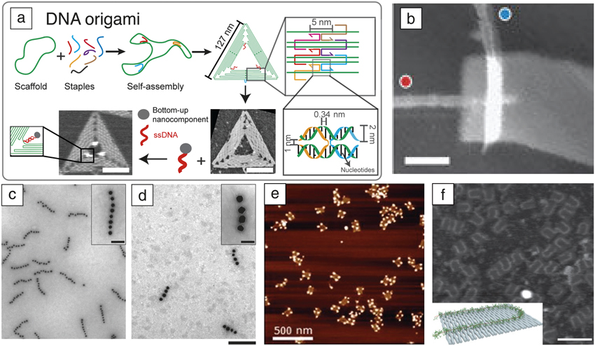
(a) Schema for synthesizing a triangular DNA origami with single-stranded binding sites on inner vertices. Atomic force microscope (AFM) images show an origami (right) before and (left) after three nanocomponents (dye molecules) were immobilized using a DNA linker. Reference Rothemund5 Scale bar = 50 nm. (b) AFM of a carbon nanotube transistor on DNA origami. Reference Maune, Han, Barish, Bockrath, Goddard, Rothemund and Winfree12 Red and blue dots indicate single-walled nanotube type. Scale bar = 50 nm. (c–d) Transmission electron microscope images of plasmonic waveguides synthesized on DNA origami. Reference Gürr, Schwarz, Ye, Diez and Schmidt9 Insets: high-resolution micrographs of waveguides. Scale bar = 200 nm; 50 nm (inset). (e) Quantum dots on DNA origami. Reference Ko, Gallatin and Liddle13 (f) Conductive polymer routed on DNA origami as potential interconnect. Reference Knudsen, Liu, Kodal, Madsen, Li, Song, Woehrstein, Wickham, Strauss, Schueder, Vinther, Krissanaprasit, Gudnason, Allen, Smith, Ogaki, Zelikin, Besenbacher, Birkedal, Yin, Shih, Jungmann, Dong and Gothelf11 Inset: Schematic showing the polymer (green) on the origami. Scale bar = 200 nm.

Key accomplishments with DNA origami, illustrated in Figure 1, include the construction of controlled metal-nanoparticle arrangements for plasmonic applications, Reference Gürr, Schwarz, Ye, Diez and Schmidt9 the creation of conductive nanowires by nucleating metal on the origami Reference Liu, Geng, Pound, Gyawali, Ashton, Hickey, Woolley and Harb10 or routing a conductive polymer, Reference Knudsen, Liu, Kodal, Madsen, Li, Song, Woehrstein, Wickham, Strauss, Schueder, Vinther, Krissanaprasit, Gudnason, Allen, Smith, Ogaki, Zelikin, Besenbacher, Birkedal, Yin, Shih, Jungmann, Dong and Gothelf11 carbon nanotube transistors, Reference Maune, Han, Barish, Bockrath, Goddard, Rothemund and Winfree12 and quantum dot nanoclusters Reference Ko, Gallatin and Liddle13 as well as single-molecule biosensors. Reference Voigt, Tørring, Rotaru, Jacobsen, Ravnsbæk, Subramani, Mamdouh, Kjems, Mokhir, Besenbacher and Gothelf14 State-of-the-art protocols allow simultaneous organization of a few distinct materials, with three-dimensional (3D) control of the layout and localization precision of ∼5 nm. While these results have clearly shown the power of DNA origami as a breadboard, there is much room for improvement before the fundamental limits of this approach are reached.
Two challenges are of particular interest: (1) improving the spatial resolution and precision of materials placement and (2) arranging materials with greater diversity in both chemical composition and shape (e.g., nanorods or nanocubes instead of nanospheres; nonspherical particles are just beginning to be explored). Reference Kuzyk, Schreiber, Zhang, Govorov, Liedl and Liu15,Reference Roller, Besteiro, Pupp, Khorashad, Govorov and Liedl16 To make these challenges concrete, consider two-material plasmonic devices (see the Pilo-Pais et al. article in this issue), Reference Pilo-Pais, Acuna, Tinnerfeld and Liedl17 both existing and an exciting type of device that has not yet been assembled on a DNA breadboard. Pairs of metal nanoparticles (e.g., gold nanorods, the first material), appropriately aligned, create a gap region with a high electric field between them. Gold–DNA coupling chemistry is well developed, so these types of devices have been created and used to enhance the fluorescence emission of molecules (the second material) positioned within the gap. Reference Zhang, Gao, Li, Lang and Xu18,Reference Acuna, Möller, Holzmeister, Beater, Lalkens and Tinnefeld19 In one case, Reference Zhang, Gao, Li, Lang and Xu18 enhancement was studied by changing the gap between rods in coarse ∼6-nm steps from 26 nm (enhancement was 120-fold) down to 6 nm (maximum enhancement of 470-fold). Much higher enhancements could have been achieved if the gap were narrowed below 6 nm, but fine control over the relative position of components is limited by several factors, including the thickness (1–10 nm) of the shells and coatings used to stabilize functional nanoparticles, the DNA linker lengths (3–10 nm) often used to couple particles and molecules to origami breadboards, and the resolution of easily modifiable positions (on a DNA origami 3–6 nm, typically at the ends of staple strands). Further, if the molecular fluorophore in the gap could be replaced by a photocatalytic TiO2 nanoparticle, the device might be used for highly efficient hydrogen production for artificial photosynthesis. In this case, similar problems would arise, as hydrogen production would depend critically on positioning of the TiO2 particle in the gap.
Overcoming these challenges in any particular instance may require custom chemistry, but we offer a few suggestions. First, with respect to spatial localization, getting rid of the intervening DNA linkers will help. In many cases, it will be possible to couple functional materials directly to site-specific modifications of the DNA backbone (explored via phosphorothioate chemistry Reference Burns, Stulz and Howorka20 ) or via internal linker-modified bases (widely available, but often more costly compared to DNA end-modification). Either approach has the potential to increase the resolution of nanomaterial position to 0.34 nm (the spacing of DNA bases along the helix), but the twist of the helix must be taken into account, and the modularity of the DNA linkers that allows the facile swapping of material type is sacrificed. Additionally, if the DNA origami were structurally stable in organic solvents, a much larger catalog of materials could be bound. For situations where only a single critical distance needs to be controlled, the use of mechanical “DNA calipers” can allow the spacing between nanomaterials to be controlled with angstrom precision. Reference Funke and Dietz21
Another direction, which could impact both spatial localization and materials diversity, would be a move to organic-phase coupling of naked functional components to the DNA breadboard. Many interesting materials are hydrophobic such that transferring them from parent solutions to aqueous solution is difficult or impossible with a DNA linker-based approach. However, attaching small organic compatible linking groups (e.g., amines, thiols, alkynes, dienophiles) to DNA origami is straightforward; more difficult is stabilizing DNA origami in organic solvents. One potential solution is to immobilize the DNA origami on a planar surface from an aqueous solution and then moving it into an organic phase through serial dilution. Reference Gopinath and Rothemund22 This approach would only apply to 2D structures. Surface coupling usually has lower efficiency compared to their solution counterparts, and salt crystals created during solvent transfer can be difficult to remove. Stabilizing DNA origami in an organic-compatible solution may prove another route. Unmodified origami form well in anhydrous ionic liquid Reference Gállego, Grover and Hud23 and charge neutralized origami coated with poly-L-lysine-poly(ethylene glycol) block copolymer Reference Ponnuswamy, Bastings, Nathwani, Ryu, Chou and Vinther24,Reference Agarwal, Matthies, Gür, Osada and Schmidt25 might be stable in organic solutions.
Lithographic organization of DNA origami
As DNA origami’s role as a breadboard has matured, a second challenge has emerged—in order to be used, most nanodevices must be integrated into multidevice architectures and interfaced with the larger macroscopic world. The problem is, whether devices are assembled first on the origami in solution or after its deposition on a surface, existing deposition methods result in random arrangements of origami (and associated devices). To connect to devices, their locations need to be mapped with scanning electron microscopy or atomic force microscopy. Such an approach is poorly suited for creating integrated systems with a large number of interconnected devices. Thus, it is crucial to develop methods for deterministic organization of DNA origami (and associated devices) on planar substrates and within top-down nanofabricated devices.
Pioneering work on the lithography-directed self-assembly of nanoparticles Reference Cui, Björk, Liddle, Sönnichsen, Boussert and Alivisatos26 was based simply on capillary trapping at topographical features. In contrast, the lithographic organization of DNA origami has emphasized chemical patterning, using both electrostatic and covalent interactions to create specific binding sites for origami. Important goals to achieve are (1) a high yield of single origami bound at desired sites, and (2) controlling the orientation of those origami, both with respect to in-plane rotation and with respect to which origami face binds a surface. Assembly of a negatively charged origami rectangle on top of a strongly positively charged self-assembled monolayer on gold islands Reference Gerdon, Oh, Hsieh, Ke, Yan and Soh27 produced results whose single-origami yield was difficult to measure and whose orientation was uncontrolled. Linear origami functionalized with thiols assembled between gold islands made point-to-point contacts with high yield, but the linear origami could not control the orientation of multicomponent 2D devices. Reference Ding, Wu, Xu, Zhao, Liu, Yu and Yan28
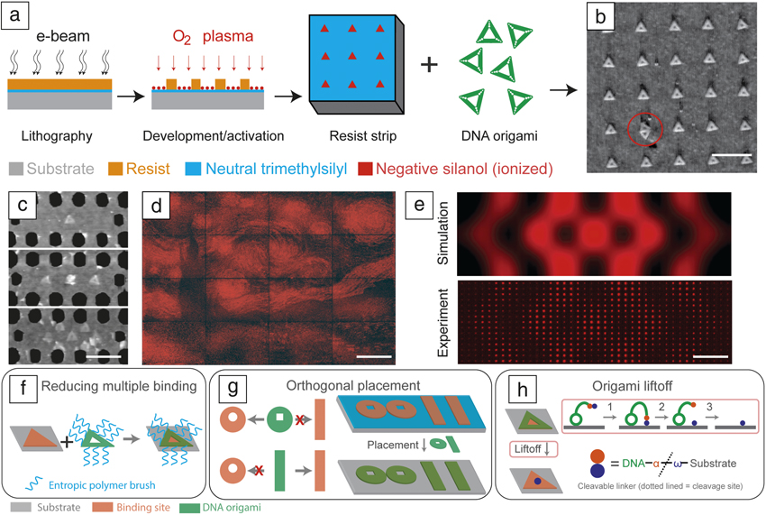
For 2D origami, strong electrostatic or covalent interactions generally result in irreversible trapping of multiple origami at a binding site or irreversible trapping in undesired orientations. Weaker, tunable electrostatic binding has been achieved between negatively charged origami and negatively charged binding sites by using Mg2+ as ionic bridges, Reference Kershner, Bozano, Micheel, Hung, Fornof, Cha, Rettner, Bersani, Frommer, Rothemund and Wallraff29 at high concentrations (125 mM). The method, termed “DNA origami placement” ( Figure 2a), enables high single-origami yield on difficult-to-source diamond-like carbon (DLC) and reasonable yield on common SiO2 substrates. Subsequent optimization (Figure 2b) of the technique Reference Gopinath and Rothemund22 has enabled high yield of single-origami binding (>95% of sites) with precise orientation (within ±10° of the desired orientation) on SiO2 at low Mg2+ (<10 mM). Covalent coupling of origami to carboxylated binding sites stabilizes them in pure water, thus current methods are compatible with large gold nanoparticles, carbon nanotubes, other materials that would otherwise aggregate in high Mg2+.
(a) Schema for the fabrication of origami binding sites on a semiconductor wafer. (b) Representative atomic force microscope (AFM) image of “origami placement” shows origami triangles bound to sites in a lithographically defined array (red circle shows multiple binding). Reference Gopinath and Rothemund22 Scale bar = 400 nm. (c) AFM of DNA origami used to position fluorophores within lithographically patterned photonic crystal cavities (PCCs). Scale bar = 400 nm. (d) Large-scale integration. Reference Gopinath, Miyazono, Faraon and Rothemund30 Scale bar = 125 μm. (e) (Top) Simulated local density of states (LDOS) for a single PCC. (Bottom) Wide-field epifluorescence microscope image from a 40 × 15 array of PCCs, each of which have the origami positioned in a different location to map the LDOS of the PCC. Scale bar = 25 μm. (f) Proposed method to reduce multiple bindings by engineering steric occlusion using polymer brushes. (g) Example of a proposed orthogonal placement process. (h) Schema for a proposed DNA origami liftoff technique involving immobilizing the origami, creating a covalent linkage, followed by cleaving the linker and removal of the origami. Note: α and ω, abstract representations of two functional groups forming the cleavable linker.
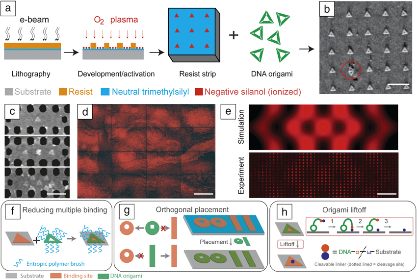
Compatible with conventional fabrication, DNA origami placement allows the integration of molecular and nanoparticle devices with microfabricated devices at the manufacturing scale. In recent work, Reference Gopinath, Miyazono, Faraon and Rothemund30 a defined number of molecular emitters (Figure 2c) were positioned in 65,536 photonic crystal cavities (PCCs) to digitally program their emission intensity (Figure 2d). Reference Gopinath, Miyazono, Faraon and Rothemund30 Precise placement of emitters (∼20 nm in x and y) into the PCCs enabled imaging of the resonant mode at a resolution far below the wavelength of light (< λ/10) when using a simple epifluorescence microscope (Figure 2e).
Several improvements to this placement method are required for application in practical technology. First, symmetric triangular origami must be replaced with asymmetric shapes that will enable devices to provide a unique orientation on the surface. Second, the current defect rate of 10–2, for multiple origami binding, must decrease; here, improved kinetic and thermodynamic models may aid the search for better assembly conditions, but experimentally, the introduction of entropic brushes Reference Martin, Wilcoxon, Odinek and Provencio31 on the origami edge may prevent multiple binding (Figure 2f). To achieve patterning of multiple device types on a wafer, it will be necessary to develop “orthogonal” shapes, which bind most strongly to shape-matched binding sites (Figure 2g). Finally, in some instances, it will be necessary to find ways to remove DNA and leave a device behind. For example, while the DNA origami placement could, in principle, be used to position single atoms at specific locations for creating quantum switches, Reference Wilk, Webster, Kuhn and Rempe32,Reference Fuechsle, Miwa, Mahapatra, Ryu, Lee, Warschkow, Hollenberg, Klimeck and Simmons33 such an approach is unlikely to be adopted since the presence of DNA origami will affect the switching behavior. Thus, the use of a cleavable linker between a device and the origami carrying it would allow removal of the origami after placement, a process analogous to metal liftoff (Figure 2h).
Pattern transfer using DNA origami
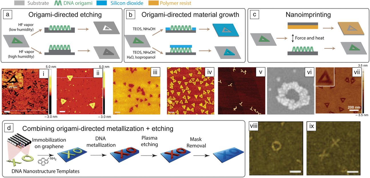
The homogeneity, complexity, and resolution of DNA origami make it an attractive alternative to nanopatterning for lithography. Unfortunately, since DNA does not possess technologically significant optical, electrical, or mechanical properties, it cannot be directly used as a functional unit. While DNA origami can be used as a breadboard to scaffold discrete heterogeneous functional materials (Figure 1), an intriguing alternative is to transfer geometric features of DNA origami directly into a bulk functional material. In this picture, DNA origami serves either to replace a traditional polymer etch resist ( Figure 3a), as a template for growth of functional material (Figure 3b), or as a master for nanoimprinting (Figure 3c).
Schematic for origami directed (a) etching, (b) material growth, and (c) nanoimprinting. (i–ii) Atomic force microscope (AFM) image of origami deposited on SiO2, which is etched using HF vapor in a high relative humidity or low relative humidity environment. Scale bars = 100 nm; color bars represent height. Reference Surwade, Zhao and Liu34 (b) Schematic showing origami-directed silicon dioxide growth controlled by relative humidity. (iii) Growth everywhere around origami. Scale bar = 250 nm. Reference Surwade, Zhou, Wei, Sun, Powell, O’Donnell, Yin and Liu36 (iv) Growth on DNA origami. Scale bar = 200 nm. Reference Surwade, Zhou, Wei, Sun, Powell, O’Donnell, Yin and Liu36 (v–vi) AFM showing metallization of DNA origami. Reference Liu, Geng, Pound, Gyawali, Ashton, Hickey, Woolley and Harb10,Reference Schreiber, Kempter, Holler, Schüller, Schiffels, Simmel, Nickels and Liedl37 (c) Schematic of nanoimprinting for pattern transfer from DNA origami to a polymer surface. (vii) AFM images of nanoimprinted DNA origami; inset: higher magnification image of origami. Color bar represents height. Reference Tian, Kim, Sun, Kim, Yin and Liu40 (d) Schematic of creating graphene nanostructures using metallized DNA origami as the etch mask, and (viii–ix) AFM images of graphene nanostructures fabricated by using metallized DNA origami as etch mask. Note: TEOS, tetraethylorthosilicate.

The main challenge for etch-based pattern transfer has been the unsuitability of traditional chemical and physical etches that quickly degrade origami or remove them from the surface. Furthermore, the 2-nm thickness of 2D DNA origami demands a highly selective etching process to ensure faithful pattern transfer. Surwade et al. Reference Surwade, Zhao and Liu34 showed that, despite these difficulties, unmodified DNA origami are stable enough to be used as an etch mask in vapor-phase HF etching of SiO2 (Figure 3i–ii); here, DNA origami change the amount of surface-adsorbed water, which is a catalyst for the HF etching reaction, thus providing a mechanism to create etch contrast. This approach has since been used Reference Diagne, Brun, Gasparutto, Baillin and Tiron35 to pattern sub-10 nm features. Analogous chemistry Reference Surwade, Zhou, Wei, Sun, Powell, O’Donnell, Yin and Liu36 has been used to modulate the rate of SiO2 chemical vapor deposition to create positive and negative patterns (Figure 3iii–iv). DNA origami have also been used for direct metallization, creating geometrically well-defined metallic structures Reference Liu, Geng, Pound, Gyawali, Ashton, Hickey, Woolley and Harb10,Reference Schreiber, Kempter, Holler, Schüller, Schiffels, Simmel, Nickels and Liedl37 (Figure 3v–vi). More simply, by excluding the binding of an adsorbent, DNA templates have been used to pattern the growth of self-assembled monolayers Reference Surwade, Zhou, Li, Powell, O’Donnella and Liu38 and to deposit protein film. Reference Busuttil, Rotaru, Dong, Besenbachera and Gothelf39 Tian et al. Reference Tian, Kim, Sun, Kim, Yin and Liu40 demonstrated DNA imprinting on various polymer substrates, opening the way to using DNA templates for soft lithography (Figure 3vii). “Molecular contact printing” has also been used to transfer protein patterns decorated on DNA origami from one surface to another. Reference Busuttil, Rotaru, Dong, Besenbacher and Gothelf41 Finally, combinations of approaches show promise: sequential metallization and plasma etching (Figure 3viii–ix) enable the transfer of DNA shapes into graphene.
Despite these advances, two barriers need to be overcome before pattern-transfer methods can yield functional nanostructures and devices. The first barrier is the lack of control over the surface arrangement of DNA origami. Although this problem has been partially solved (Figure 2), lithographic organization of DNA origami and origami-driven pattern-transfer methods have not yet been combined. Such a step would be a landmark achievement, validating multistep DNA-based patterning in the context that would enable device integration. The second major barrier is the low-aspect ratio of DNA-patterned structures. So far, origami-assisted etching or material growth have yielded features with a vertical profile of only a few nanometers, while top-down features can have vertical profiles that are micrometers deep. Figure 4 illustrates proposed methods to overcome or sidestep this barrier.
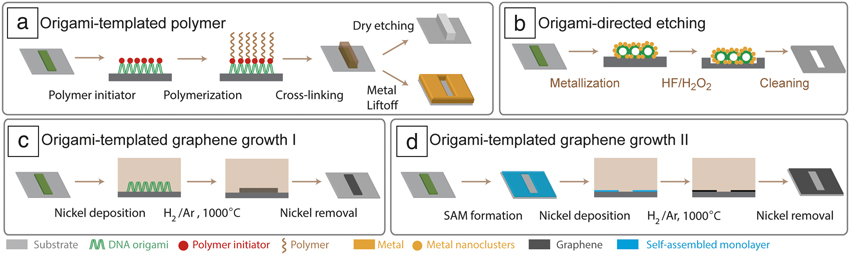
(a) Schema for converting an immobilized DNA origami into a geometrically well-defined polymer island that can, in turn, be used in top-down processes such as liftoff or dry etching. (b) Schema for metallization of DNA origami for use in metal-assisted catalytic etching. (c) Schema proposing the conversion of DNA origami into a graphene bilayer nanoisland using metal catalysis. (d) Schema illustrating the creation of a self-assembled monolayer (SAM) using DNA origami that is then converted into graphene using metal catalysis.
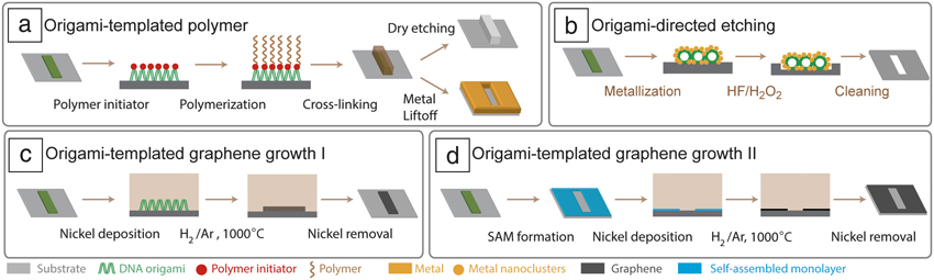
The first approach involves converting a DNA origami carrying polymerization initiators into a better resist by established surface polymerization methods (Figure 4a). After the polymer has amplified the height of the origami, the resulting feature can be used as an etch or liftoff mask. Tokura et al. Reference Tokura, Jiang, Welle, Stenzel, Krzemien, Michaelis, Berger, Barner-Kowollik, Wu and Weil42 took initial steps in this direction by growing poly(ethylene glycol) methyl ether methacrylate from initiators bound to specific locations on the origami. However, growing a standard resist, such as poly(methyl methacrylate) (PMMA), Reference Discekici, Pester, Treat, Lawrence, Mattson, Narupai, Toumayan, Luo, McGrath, Clark, de Alaniz and Hawker43 may be better since existing optimized etch or liftoff strategies could be used.
A second route to create deep features is metal-assisted catalytic etching (MACE). Reference Huang, Geyer, Werner, De Boor and Gösele44 MACE is a wet, but directional, etch technique used to create anisotropic, high-aspect-ratio micro-/nanostructures in Si or III–V compound semiconductors. MACE relies on a noble metal (Au, Pt, or Ag) to trigger local oxidation, leading to etching of the semiconductor under the metal features. Figure 4b shows how MACE can be used with DNA origami.
Instead of creating deep features in a semiconductor material, DNA origami could be used to directly form extremely thin 2D materials such as graphene or MoS2. Figure 4c–d shows two proposed approaches to create graphene nanostructures. The first method (Figure 4c) uses surface-immobilized DNA origami as the source of carbon to create a graphene bilayer, which is a semiconductor, via a well-established protocol. Reference Sun, Yan, Yao, Beitler, Zhu and Tour45 With this approach, the phosphate and nitrogen groups in DNA may induce impurities. In a second approach (Figure 4d), DNA origami is used to template a self-assembled monolayer that can then be used as a carbon source for graphene formation without inducing impurities. Both approaches potentially enable the creation of graphene with smaller features and fewer edge defects. Initial efforts using Al2O3-capped DNA origami Reference Zhou, Sun, Ricardo, Wang, Shen, Yin and Liu46 has shown that origami shapes can be preserved through the carbonization process.
What lies ahead
From the early days of DNA nanotechnology until recently, an argument has been made that the 2-nm width of the DNA helix and the 0.34-nm spacing of the bases might allow the bottom-up self-assembly of circuits with features not achievable by any top-down techniques. This resolution argument does not seem compelling today. We have discussed the difficulties with achieving better than 5-nm resolution using DNA structures, and the resolution of today’s complementary metal oxide semiconductors is quickly closing in—7-nm features are already in commercial production and features as small as 4 nm are expected in the next five to six years. Thus, we propose that bottom-up DNA-based fabrication will find its greatest application in technologies that are challenging for conventional fabrication.
Conventional fabrication has traditionally excelled at planar structures, and only recently have serious attempts been made to develop 3D circuits via top-down methods, introducing complex schemes for alignment between layers. Reference Lee, Chen and Lu47 Bottom-up methods have the advantage that self-assembly can intrinsically provide alignment between devices as they are grown upward into the third dimension. Thus, one area where the combination of DNA origami with top-down nanofabrication may prove advantageous is the fabrication of high-density 3D integrated circuits. Figure 5 shows a schema for constructing such a circuit, starting with placement of a flat 2D origami on top-down fabricated metal contacts (Step 1). Next, two origami cylinders are sequentially attached; one carries an n-type and the other a p-type semiconductor to form a vertical p–n junction. Finally, an insulating layer and metal contacts are grown by targeted mineralization and metallization to yield a single vertical p–i–n junction. The same process could be performed in parallel at multiple surface sites and repeated iteratively to form 3D circuit arrays. Only the first step has been demonstrated, and thus, much work remains, including the development of high-yield nanoparticle–DNA coupling for multiple materials and techniques to create efficient metal contacts.
Schema showing DNA origami-assisted nanofabrication of a high-density 3D electronic circuit.

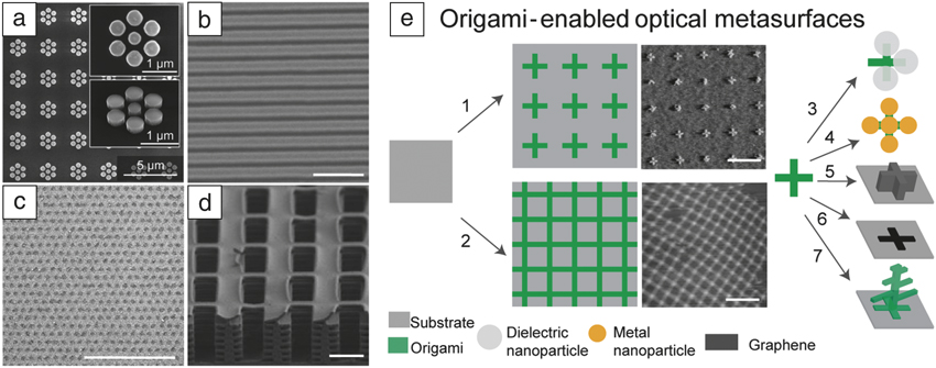
A second class of applications that may benefit from DNA-based fabrication are those that require vast areas of substrates to be patterned at the nanoscale, but require little integration and can tolerate high defect densities. Such applications might be viewed as forms of “nanostructures paint,” the most exciting of which are currently planar optical metasurface Reference Yu and Capasso48 —arrays of microscopic light scatterers whose overall optical properties emerge from microscale structures, depending strongly on both individual scatterers and their spatial arrangement. The structural color of a butterfly wing provides a striking example of an optical effect arising from a natural metasurface. Artificial metasurfaces include clusters of metal nanoparticles Reference Chong, Hopkins, Staude, Miroshnichenko, Dominguez, Decker, Neshev, Brener and Kivshar49 ( Figure 6a), graphene ribbons, Reference Yan, Low, Guinea, Xia and Avouris50 or nanodisks Reference Fang, Wang, Schlather, Liu, Ajayan, García de Abajo, Nordlander, Zhu and Halas51 whose properties can be controlled using an electric field (Figure 6b–c); or surfaces that mimic the properties of butterfly wings Reference Zhang and Chen52 (Figure 6d). Metasurfaces promise unprecedented control over light and are typically envisioned for use in large-area applications such as windows and solar cells. However, current metasurface fabrications rely upon top-down techniques that are unsuitable for mass production. Roll-to-roll nanoimprinting may be viable, but it still requires expensive equipment and changing device design that requires a costly new master, and it is difficult to mix different optical materials within the same structure. A DNA origami-centered approach, on the other hand, would be ideally suited for this kind of application.
(a) Scanning electron microscope (SEM) micrograph of an optical metasurface created by metal nanoparticle clusters; Reference Chong, Hopkins, Staude, Miroshnichenko, Dominguez, Decker, Neshev, Brener and Kivshar49 (b–c) SEM micrographs of electrically tunable optical metasurfaces created by graphene (b) nanoribbons Reference Huang, Geyer, Werner, De Boor and Gösele44 or (c) nanodisks. Reference Fang, Wang, Schlather, Liu, Ajayan, García de Abajo, Nordlander, Zhu and Halas51 Scale bar = 1 μm. (d) SEM micrograph of lithographically fabricated surface that mimics the structural color properties of a blue morpho butterfly. Reference Zhang and Chen52 Scale bar = 1μm. (e) Two approaches (1–2) to assemble DNA origami into periodic patterns by lithography directed assembly or surface crystallization; Reference Suzuki, Endo and Sugiyama55 (3–7) are different methods to create light scatterers using DNA origami. Scale bars = 400 nm.
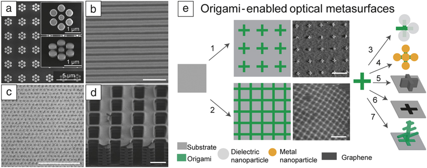
For the purpose of prototyping metasurfaces, DNA origami can be organized using e-beam lithography (Figure 2 and Figure 6e, arrow 1). For the purpose of economically covering large areas, DNA origami can be crystallized in solution and deposited (Figure 6e, arrow 2), Reference Tikhomirov, Petersen and Qian53,Reference Liu, Zhong, Wang and Seeman54 or crystallized on the surface. Reference Suzuki, Endo and Sugiyama55–Reference Rafat, Pirzer, Scheible, Kostina and Simmel57 With respect to origami synthesis, cost will not be an obstacle for high-tech applications. By genetically encoding both scaffold and staple strands, it now requires just seven liters of culture to yield a gram of DNA origami and, at the 800-liter scale, total costs, including equipment, labor, and energy are USD$200 per gram. Reference Praetorius, Kick, Behler, Honemann, Weuster-Botz and Dietz6 A single gram of DNA origami can cover 1000 m Reference Xia and Whitesides2 , more than three tennis courts in area. Equal in importance to cost is the large diversity of metasurfaces that origami will enable, encompassing both current metasurfaces, such as those based on simple clusters of nanoparticles (Figure 6e, arrows 3–4), and new metasurfaces based on scatterers that are difficult to create without origami, such as 3D dielectric shapes (Figure 6e, arrow 7).
From the work we have highlighted, and applications we have proposed, it is clear that the merger of DNA origami with conventional fabrication is still in its infancy. It will take the concerted effort of lithographers, materials chemists, and device physicists to demonstrate large-scale device integration, expand materials diversity, and find the applications for which the unique advantages of DNA origami are most suited. Regardless of the applications that emerge, DNA origami uniquely stands as the only method currently available to modularly bridge top-down and bottom-up nanofabrication.
Acknowledgments
A.G. acknowledges support from the Office of Naval Research Award N000141410702, National Science Foundation Grant Nos. 1636364 and 1317694 (Expedition in Computing, Molecular Programming Project, http://molecular-programming.org. A.T.W. acknowledges support from the NSF CMMI Grant 1562729. M.A.K. acknowledges the Academy of Finland (Project Number 308578). H.L acknowledges support from the Office of Naval Research Award N000141512520.

Anqin Xu is a graduate student in the Department of Chemistry at the University of Pittsburgh. She graduated in 2013 with a bachelor’s degree in chemistry from the College of Chemistry and Molecular Engineering, Peking University, China. Her current research focuses on DNA-based nanofabrication, including, but not limited to, nanoscale pattern transfer from DNA nanostructures to inorganic materials. Xu can be reached by email at anx3@pitt.edu.

John N. Harb is the J.J. Christensen Professor of Chemical Engineering in the Ira A. Fulton College of Engineering and Technology at Brigham Young University, where he recently completed a term as associate dean. His research focuses on electrochemical engineering, with interests in energy-storage devices, micro- and nanofabricated electrochemical devices and structures, the fundamental processes that govern corrosion and electrodeposition, and modeling of electrochemical systems. He has co-authored two textbooks, a textbook for first-year students in chemical engineering and a soon-to-be-published text on electrochemical engineering. Harb can be reached by email at john_harb@byu.edu.

Mauri A. Kostiainen is an associate professor in the School of Chemical Engineering at Aalto University, Finland. He obtained his MSc degree in organic chemistry from the University of Helsinki, Finland, in 2005, and his PhD degree in engineering physics from the Helsinki University of Technology, Finland, in 2008. His research interests focus on the integration of biological and synthetic building blocks in a designed manner to create biohybrid materials. He has authored more than 50 articles and his awards include the TES Young Investigator Award and the World Cultural Council Special Recognition for international impact. Kostiainen can be reached by phone at +358505300027 or by email at mauri.kostiainen@aalto.fi.

William L. Hughes is an associate professor in the Micron School of Materials Science and Engineering, co-founder and associate dean of the College of Innovation and Design, and head of the Vertically Integrated Projects Program at Boise State University. He received his PhD degree in materials science and engineering from the Georgia Institute of Technology. His current research interests include DNA nanotechnology, nucleic acid memory, and synthetic biology. Hughes is the recipient of numerous awards, including the National Academy of Engineering Center for the Advancement of Scholarship on Engineering Education Award, NIH Quantitative Development K25 Career Award, and the W.M. Keck Foundation Award. Hughes can be reached by phone at +12084264859 or by email at willhughes@boisestate.edu.

Adam T. Woolley is a University Professor in the Department of Chemistry and Biochemistry at Brigham Young University. His current research focuses on biotemplated nanofabrication, creation of integrated microfluidic systems for enhanced biomarker analysis, and design of simple miniaturized biomolecular assays. He is the recipient of a Presidential Early Career Award for Scientists and Engineers (2006), the ACS Division of Analytical Chemistry Award for Young Investigators in Separation Science (2007), and the AES Mid-Career Award (2015). Woolley can be reached by email at atw@byu.edu.

Haitao Liu has been an associate professor in the Department of Chemistry at the University of Pittsburgh since 2016. He received his bachelor’s degree in chemistry in 2001 from the University of Science and Technology of China. He was a graduate student at the University of California, Berkeley, and obtained his PhD degree in chemistry in 2007. He completed postdoctoral research at Columbia University. In 2010, he joined the Department of Chemistry at the University of Pittsburgh as an assistant professor. His research interests include DNA-based nanofabrication, surface properties of graphitic materials, and reaction mechanisms of the synthesis of inorganic colloidal nanocrystals. Liu can be reached by email at hliu@pitt.edu.

Ashwin Gopinath is a research scientist in the Department of Bioengineering at the California Institute of Technology. He obtained his PhD degree in electrical engineering from Boston University in 2010. His research is focused on developing scalable techniques to organize single molecules, quantum optics, tools for single-molecule biophysics, and nanoparticle therapeutics. Gopinath can be reached by email at ashwing@caltech.edu.