I. INTRODUCTION
Global video traffic over the Internet is forecast to reach 80% of the global IP traffic by 2019 from 67% in 2014. The increasing popularity of video-on-demand (VoD) in ultra-high definition necessitating about 18 Mbit/s bit rate, thus nine times more than standard definition video streaming, forecast to reach 21% of the global VoD traffic by 2019 results in an ever-increasing load on data centers to fast delivery of services and data [1]. Furthermore, according to [2], more than 75% of the total data traffic are within the data center. This traffic is enabled by high-performance servers interconnected by multiple switching networks [Reference Okamoto3]. The data rate (DR) of this short-to-medium interconnect is in the range of 25 Gbit/s in year 2014 [Reference Takemoto, Yamashita, Yazaki, Chujo, Yong and Matsuoka4].
Using electrical interconnects at these DRs necessitates compensation of the high insertion losses as well as the reflections done at the cost of a high-power consumption and an increased circuit complexity with a high-order decision-feedback equalizer [Reference Toifl5]. Fiber-optic interconnects offer a power efficient alternative due to their lack of reflections, weight, high channel bandwidth (BW), and low attenuation, which makes them suitable to transmissions up to hundreds of meters [Reference Takemoto, Yamashita, Yazaki, Chujo, Yong and Matsuoka4, Reference Pan6].
A further trend is to integrate the complete unit into one silicon substrate. The advancement of complementary metal–oxide–semiconductor (CMOS) technologies makes it possible to have the digital data-processing core in the same system-on-chip (SoC) with the analog interface and supply circuits, reducing the overall costs and performance degradation [Reference Schow7]. In case of high-speed analog frontends, the BW is a key requirement. Its enhancement necessitates often inductive peaking with inductors occupying a significant area [Reference Okamoto3–Reference Huang10]. As the cost of manufacturing deep sub-micron CMOS technologies is extremely high, the area is nowdays among the most important considerations when evaluating an analog circuit from the mass-production cost perspective. To optimize the area, only active-peaking methods were employed in the presented design. Another important challenge in the design of electro-optical frontends in sub-micron CMOS is the high DC bias and operation voltage of electro-optical components. Modulators and vertical cavity surface-emitting laser (VCSEL) diodes need to be operated at voltages, which are multiples of the breakdown voltage of CMOS technologies. Special architectures are used, such as in [Reference Szilagyi, Belfiore, Henker and Ellinger11], to provide the necessary DC bias to the VCSEL but not exceed the breakdown voltage of individual transistors.
The architecture of the electro-optical frontend consisting of a receiver (RX) and a laser diode driver (LDD) is presented in Section II. Section III discusses the design challenges, dimensioning of the devices, and simulation result of each block of the RX frontend. As active peaking was used extensively to increase the BW and gain of the circuits, the mechanism of this method is analyzed. In Section IV, the design and simulation result of the LDD is described. The circuit was fabricated in a 28 nm super low-power (SLP) digital CMOS process. Electrical measurements evaluate the small-signal performance of both the RX and the LDD in Section V. Electro-optical measurements are performed on the chip on a printed circuit board (PCB), bonded to a commercial photo diode (PD) and a VCSEL. Optical signal-integrity measurements show an error-free operation with a bit error rate (BER) of 10−12 up to a DR of 20 Gbit/s of the RX and 25 Gbit/s of the LDD. Finally, the results of both the RX and the LDD are compared with existing designs in the “Conclusion” section.
II. ARCHITECTURE OF THE ELECTRO-OPTICAL FRONTEND
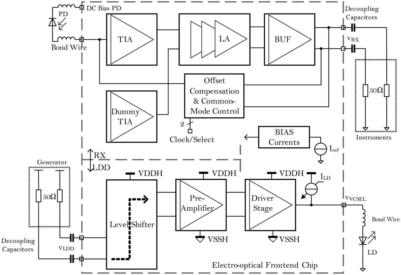
The electro-optical frontend consists of two main parts, the RX and LDD as depicted in Fig. 1. In addition, there are bias, logic, and electrostatic discharge protection circuits. A PD with 190 fF is bonded at the input of the RX with additional 30 fF of pad capacitance. A transimpedance amplifier (TIA) converts the current generated by the PD into a voltage. In order to have a signal amplitude in the hundreds of mV range, the signal is further amplified by the limiting amplifier (LA) consisting of three cascaded differential stages. Since the TIA is single-ended and the LA differential, a dummy TIA provides the common-mode (CM) signal at the other input of the LA. For measurement purposes, the output of the LA should be matched to 50 Ω and a single-ended voltage swing of at least 200 mV should be provided on a 50 Ω load. For this reason, a buffer (BUF) is used, supplied from a separate power supply, VDDB.
Block diagram of the single-chip electro-optical frontend.

There are two challenges when considering the design of a RX for optical communications. First, the DC current caused by the average optical light, which can change depending on the data pattern as well as the transmission medium. This current, present at the input of the TIA, can cause the DC-operating points of the TIA and LA to shift. This influence can go as far as entirely hinder the functionality of the RX. The second consideration is the effect of process variation and mismatch on the amplifier. Offset can cause the same issues as the DC current. When this offset is amplified, the differential output becomes unbalanced, thus clipping the signal. The amount of unbalance can be so high that the outputs stick to the upper and lower limits, thus no signal can be seen. To overcome these two issues, the offset compensation (OC) and common-mode control block was added to the RX. The input of the TIA is adjusted if offset is measured at the oputput of the RX.
The common-cathode (CC) LDD, as depicted in the lower half of Fig. 1, consists of a level shifter, a pre-amplifier, and the driver stage. In order to be able to provide the DC bias voltage to the anode of the VCSEL, the LDD is supplied from a high-voltage (HV) supply VDDH. The pre-amplifier and the output stages have VDDH as positive supply; however, the negative supply is not the global VSS but a floating VSSH which is 1.2 V lower than VDDH. The signal is transfered to the HV domain by the level shifter. This block provides an isolation between the two voltage domains. At the output, a current source is used to tune the DC current through the VCSEL.
The presented electro-optical frontend is implemented in a 28 nm SLP digital CMOS process. As this is a technology optimized for digital circuits, the performance of high-speed analog circuits is lower than those realized in silicon on insulator (SOI) CMOS [Reference Rylyakov12] or BiCMOS [Reference Xuan, Ding, Liu, Baehr-Jones, Hochberg and Aflatouni13] technologies. Furthermore, the devices in SLP are intended for low-power digital design, thus more challenging for analog high-speed design than, for example, high-performance bulk CMOS processes that have dedicated devices for analog circuits. It is however more convenient to implement high-density digital circuits such as processors and digital signal processing blocks in bulk SLP CMOS. The presented frontend can be then integrated on a single SoC with the high-density digital blocks.
III. DESIGN OF THE OPTICAL RECEIVER
A) Transimpedance amplifier
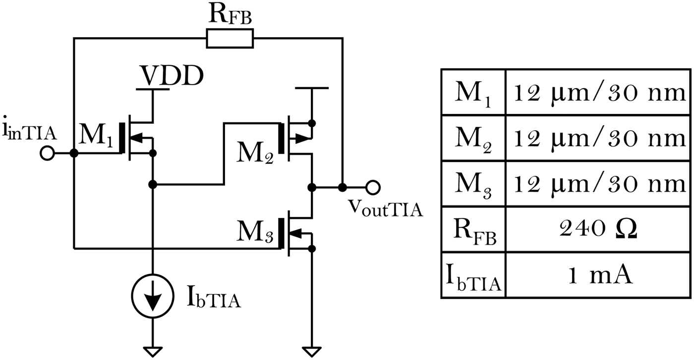
The schematic of the TIA is shown in Fig. 2. As the supply voltage is low, so the voltage headroom for stacking devices is modest, a shunt-feedback topology was preferred instead of a common-gate TIA. The transimpedance gain is set by R FB . This topology has the trade-off between the input impedance, defining the BW which is inversely proportional – and the gain that is proportional to R FB . Thus, a compromise must be made when selecting the R FB , so that the BW of the TIA is in accordance with the maximum BW of the following blocks. With this regard, R FB is chosen to 240 Ω, and with a total input capacitance of the PD and a pad of 220 fF, a BW of 12 GHz can be reached in simulation.
Schematic diagram of the TIA.

Transistors M 2 and M 3 form a CMOS inverter-type amplifier stage as in [Reference Okamoto3, Reference Pan6, Reference Li8, Reference Proesel, Schow and Rylyakov14, Reference Pan15] when both transistors are in saturation. The gain of this stage can be written as
 $$A_{v,M_2 + M_3} = - (g_{m,M_2} + g_{m,M_3} ) \times (r_{DS,M_2} {\rm \parallel} r_{DS,M_3} ).$$
It can be seen in equation (1) that in order to increase the open-loop gain of the TIA, which would decrease its input resistance as a result of increase of BW, the transconductances
 $g_{m,M_2} $
and
 $g_{m,M_3} $
need to be as high as possible. By increasing the area of M
2 and M
3, the g
m
would indeed increase; however, the input capacitance would also be higher, thus reducing the BW. Instead, a common-drain (CD) stage M
1 is added to shift the input voltage to a lower value, thus increase the
 $V_{GS,M_2} $
. Another beneficial effect of adding M
1 is the decreasing of the capacitance at the input of the TIA by splitting the Miller capacitances created by the gate–drain capacitances of M
2 and M
3, so only half is seen at the input node. Meanwhile, a pole and zero are created at high frequencies at the source of M
1. The open-loop gain of the TIA calculated with equation (1) matches the simulated gain of −4.6. The power consumption of the TIA is 4.5 mW.
B) Limiting amplifier
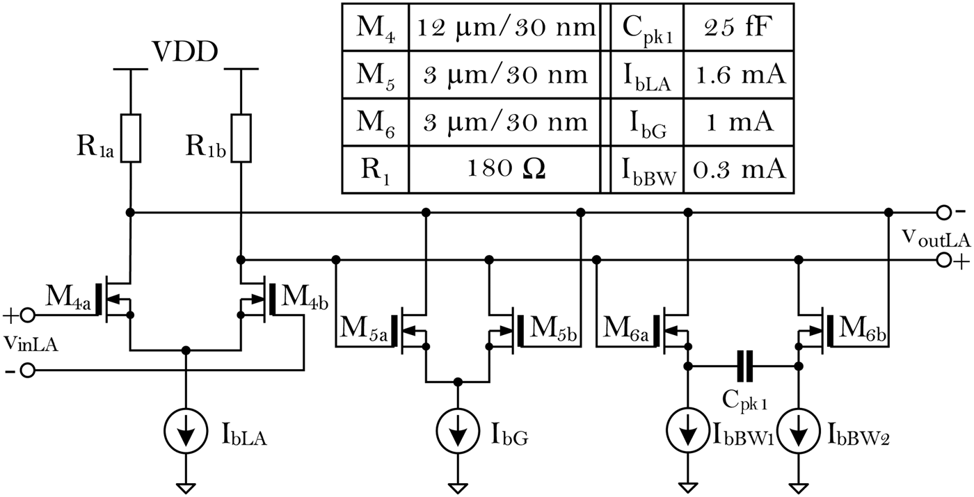
To have a signal swing of 400 mV pp , the output voltage at the TIA needs to be further amplified. Since the signal format is non-return to zero, only the low and high levels are important, thus a LA is suitable. Given the low supply voltage and intrinsic gain of the devices, both gain and BW-enhancing techniques must be implemented. Using them, the required gain of around 20 dB can be reached with three cascaded stages. The schematic of one LA stage is depicted in Fig. 3. Transistors M 4a and M 4b together with R 1a and R 1b form a differential amplification stage. The gain is enhanced by M 5a and M 5b , while the BW is boosted using M 6a , M 6b , and C pk1. The most straightforward way to increase the gain would be to use a higher resistor for R 1a, b which would however result in the decrease of BW and output CM affecting the next stage. For this reason, the gain boosting technique from [Reference Han, Yoo, Lee, Park, Oh and Park16] is used. The gain will change from − g m,M4a,b R 1a,b by adding the positive feedback stage with M 5a and M 5b to
 $$A_{v,LA} = - \displaystyle{{g_{m,M4a,b} R_{1a,b}} \over {1 - (g_{m,M5a,b} R_{1a,b} /2)}}.$$
Schematic diagram of a LA stage.

The gain is enhanced by increasing the load resistances of the differential stage. The highest gain can be reached when 2/g m, M5a,b is close to R 1a,b . However, g m, M5a,b should not reach the maximum value since this would cause transistors M 5a and M 5b to latch. Equation (2) yields a gain of −2.55, confirmed by simulation. With the presented technique, the gain is increased by 35%, from −1.6.
To boost the BW, the stage consisting of transistors M 6a , M 6b , and capacitor C pk1 is added. This block boosts the gain in a similar way to M 5a,b , but it becomes active only with capacitor C pk1. In other words, this stage introduces a zero to
 $$\omega _z = \displaystyle{{g_{m,M6a,b}} \over {C_{gs,M6a,b} + 2C_{pk1}}}. $$
In the stage from Fig. 3, the zero will be at approximately 11 GHz. When the total capacitance at the output node C L is larger than C pk1, ω z will create a peak in the transfer function, which will be lower than the dominant pole. Nevertheless, it is important that the zero ω z comes always before the dominant pole in order to maintain the LA stable. In order to ensure this
 $$g_{m,M6a,b} \lt \displaystyle{{C_{gs,M6a,b} + 2C_{pk1}} \over {((R_{1a,b} )/(1 - (g_{m,M5a,b} R_{1a,b} /2)))(C_{pk1} - C_L )}}$$
must be satisfied [Reference Han, Yoo, Lee, Park, Oh and Park16]. In the most conservative case, g m, M6a, b must be according to equation (4) <4 mS, thus I bBW1,2 is set to 0.3 mA.
Simulations on the LA consisting of three cascaded stages from Fig. 2 were performed. The LA consumes 13.2 mW power while having 25 dB gain and 16.4 GHz of BW.
C) Output buffer
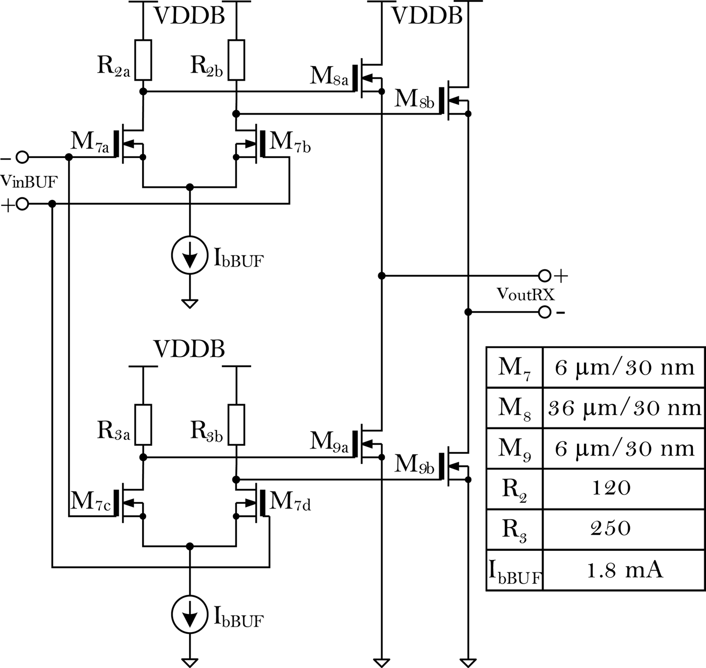
Since the electro-optical frontend is a stand-alone chip, it needs an interface that is able to drive the 50 Ω transmission lines and measurement equipment. The LA can not provide enough current to reach a reasonable voltage swing on the 50 Ω for which reason an output BUF must be used. In SoCs, the RX is connected to the clock–data recovery block and a BUF is not required, so the energy needed by the BUF is not included in the overall power balance. As it can be seen in Fig. 4, a separate power supply is used for the output BUF, VDDB. A broadband matching is achieved to 50 Ω by the output stage consisting of common-source (CS) stage M 9a, b and CD stage M 8a, b in push–pull configuration [Reference Kromer17]. The output resistance is approximately equal to
 $$R_{out,RX} = \displaystyle{1 \over {g_{m,M8a,b}}}, $$
resulting in an R out, RX of 30 Ω. In order to decrease the capacitive load on the output of the LA a pre-amplifier is added. Two differential stages with different output CMs provide the signal to the CS and CD stages. The gate voltage at M 8a,b is higher than that at M 9a,b , so the CM of the V outRX is approximately VDDB/2.
Schematic of the output BUF.

The BUF consumes 13 mW power from the supply VDDB in simulation. On a 50 Ω, the differential gain is −4 dB with approximately 60 GHz BW. The reflection coefficient is less than −20 dB up to the frequency of interest of 20 GHz.
D) Offset compensation and common-mode control
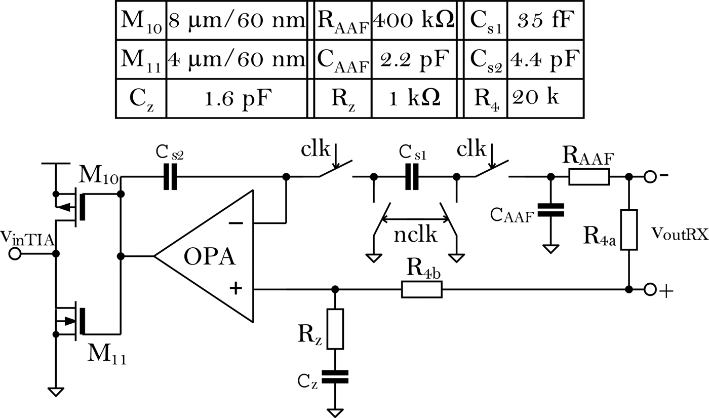
As already mentioned in Section II, the PD creates a DC current, which needs to be sunken. This current might drift in time and depends on several factors such as the bit pattern, transmission medium as well as temperature. When no circuit is available to sink this current, the operating point of the TIA will change, resulting in an offset voltage at the output. Furthermore, process variation and mismatch cause offset of the CM, especially in the LA. When amplified, the offset can drive the output out of saturation and even clip it, thus interfering with the functionality of the RX. The OC block from Fig. 5 solves this problem. As in [Reference Takemoto, Yamashita, Yazaki, Chujo, Yong and Matsuoka4], [Reference Pan6], or [Reference Huang10] a feedback loop is used to measure the offset of the CM at the output and adjust the input in order to minimize the error. All these feedback mechanisms use an RC filter. However, as it is shown in [Reference Szilagyi, Belfiore, Henker and Ellinger18], a switched-capacitor (SC) filter needs a much smaller area.
Schematic diagram of the OC block.

The OC loop works as follows: the output, differential CM is measured by R 4a and R 4b as v outCM = (v outRX+ + v outRX−)/2. The high-frequency phase shift is filtered by R z and C z [Reference Knochenhauer, Wolf, Sedighi and Ellinger19]. v outCM is then compared with the CM of v outRX− obtained by low-pass filtering (LPF) the output signal. The error is minimized by pushing or pulling current from/to the input of the TIA with transistors M 10 and M 11.
A LPF in the SC technique is used to extract the CM of v outRX− as in [Reference Szilagyi, Belfiore, Henker and Ellinger18]. The residual offset can be approximated by V os,res = V os /(1 + A v,RX + A v,OPA ), which means that A v, OPA should be maximized. However, the lower cut-off frequency of the RX f l,RX = A v,OPA × f LPF , thus a compromise between V os,res and f l, RX needs to be made. For a pseudo-random bit sequence (PRBS) of 231 − 1, f l,RX should be lower than 200 kHz. The f −3 dB of the SC filter from Fig. 5 can be expressed as
 $$f_{l,LPF} = f_{clk} \displaystyle{{C_{s1}} \over {C_{s2}}}. $$
This SC filter needs an anti-aliasing filter (AAF) with f AAF < f clk /2, where f clk is the clock frequency. It can be seen that the larger the f clk the smaller the area occupied by the AAF. Nevertheless, according to equation (6), a high f clk implies also a large area occupied by the SC filter capacitor C s2. As a good compromise, f clk was set to be at least 5 MHz and can be slightly increased if the signal pattern allows it. The resulting f AAF should be at least 2.5 MHz, although 1.2 MHz was rather implemented for a lower clock feedthrough. Given the fact that 35 fF is the smallest capacitor available in the technology, the ratio C s1/C s2 was set to 125.
Simulations with the complete RX show the lower cut-off frequency is 40.5 kHz for a 5 MHz clock and 76 kHz for 10 MHz f clk . A very small ripple can be seen on the output due to the clock feedthrough in the OC filter. The lower f clk the higher the ripple, still, it is always in the μV domain.
IV. DESIGN OF THE LASER DIODE DRIVER
Commercial VCSEL diodes need typically 1.8–2.5 V DC bias voltage and are often developed by vendors in CC configuration [Reference Szilagyi, Belfiore, Henker and Ellinger11, Reference Sedighi and Scheytt20, Reference Tsunoda, Sugawara, Oku, Ide and Tanaka21]. When a 3.3 V supply voltage as in [Reference Sedighi and Scheytt20] or [Reference Tsunoda, Sugawara, Oku, Ide and Tanaka21] is not possible, different techniques have to be applied to supply the signal at the anode of the VCSEL, meanwhile having it biased at a sufficient DC voltage. Transistors can be stacked to reach multiples of breakdown voltages. This is a technique common for drivers in CMOS such as [Reference Yazaki, Chujo, Yamashita, Takemoto, Yong and Matsuoka22], [Reference Chujo23], or [Reference Chen, Gong, Yao and Tian24]. However, this technique is sensitive to start-up sequences and might breakdown on transient peaks. The LDD placed in a triple-well topology is implemented and further developed [Reference Szilagyi, Belfiore, Henker and Ellinger11, Reference Belfiore, Szilagyi, Henker and Ellinger25].
It has to be mentioned that CC VCSEL drivers will inherently consume more power than common-anode (CA) drivers. This comes from the need of CA drivers to be supplied at much higher voltages, above the DC threshold of the VCSELs, which have their cathode connected to ground and driven on the anode terminal. On the other hand, CA drivers do not need a high-supply voltage as they drive the VCSEL at the cathode while the anode is the only terminal of the circuit, which requires a HV supply.
A) Level shifter
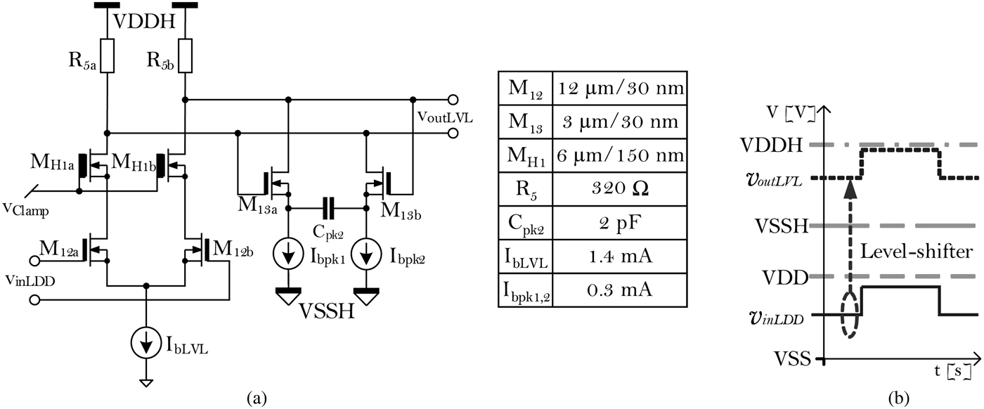
Since the pre-amplifier and output stages are in a floating well, the current-mode logic (CML) signal coming from a GND and VDD referenced generator needs to be transfered to the HV domain. This operation is done by the level shifter depicted in Fig. 6(a). The differential pair M 12a and M 12b transforms the input signal v inLDD in a current, which is transformed back into a voltage by resistors R 5a and R 5b . As it can be seen in Fig. 6(b), the output signal v outLVL is a CML signal between VDDH and VSSH. HV transistors with thick oxide M H1a,b have a breakdown voltage of approximately 2.5 V and their role is to protect the drain potential of M 12a,b from exceeding 1.2 V. I bLVL and R 5a,b are dimensioned in such way that the v outLVL CM never goes under the potential of VSSH, thus the circuits in the well are protected from overvoltage.
(a) Schematic diagram of the level shifter. (b) Functionality of the level shifter.

A similar peaking method as in the LA, a positive feedback at the frequency set by C pk2, is used to extend the BW of the level shifter. Simulations show 33.5 GHz of BW while consuming 6.2 mW of power from the 2.7 V VDDH supply.
B) Pre-amplifier and output stage
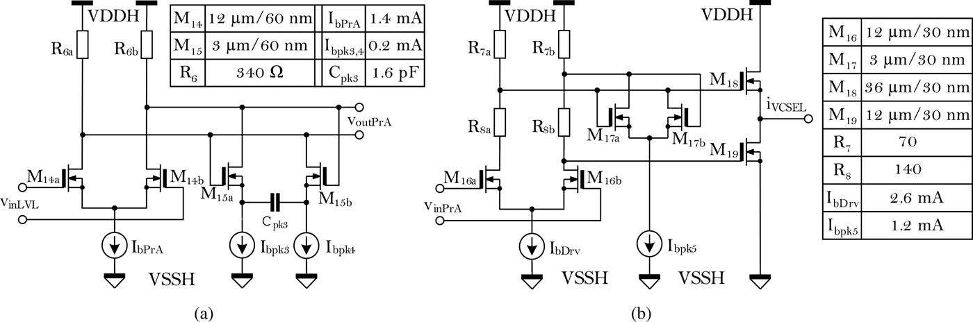
Transistors in the circuits from Fig. 7 are low-voltage, thin oxide devices, but since they are placed in a floating well, VDDH can be as high as 2.7–2.9 V, thus having an output DC voltage of more than 2 V. The local ground, which is the potential of the well, is VSSH = VDDH − 1.2 V, thus at 1.5 V. The pre-amplifier in Fig. 7(a) further amplifies the signal, driving it above a certain level in limitation. Peaking is realized by positive feedback with transistor M 15a,b at the frequency given by C pk3.
Schematic diagram of (a) the pre-amplifier and (b) the LDD output stage.

A totem-pole structure is used for the output stage as it can be seen in Fig. 7(b), in order to achieve an increased efficiency as in [Reference Szilagyi, Belfiore, Henker and Ellinger11, Reference Kromer17, Reference Belfiore, Szilagyi, Henker and Ellinger25]. Since many of the commercial VCSELs have 50 Ω impedance, the driver stage should have an output impedance of 50 Ω for an efficient power transfer. As Z out, LDD ≈ 1/g m, M18, the size of M 18 is three times of M 19. Furthermore, the DC bias of the gate is set much higher than that of M 19, to obtain a higher g m,M19. In order to compensate for the smaller gain on the high side of the totem pole, so the CD stage M 18, a gain boosting is realized with the positive-feedback cell of M 17a,b as already explained in Section III.
Small-signal simulations, considering a VCSEL diode with 300 fF capacitance and 50 Ω resistance, show that the LDD has a BW of 17 GHz and a gain of 6 dB, while 16 mW of power is consumed from the 2.7 V VDDH. Transient simulations show that the LDD modulates 6 mA pp current through the 50 Ω VCSEL diode. The bottle neck of the LDD is the output stage where on one hand large transistors are needed in order to provide enough current swing through the VCSEL, while on the other hand they have a large capacitance which slows down the driver.
V. MEASUREMENT RESULTS
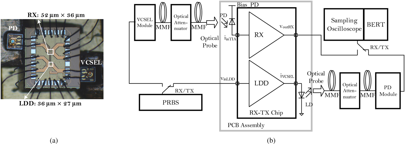
The fabricated die can be seen in Fig. 8(a). It has 0.64 × 0.9 mm2, size defined by the DC and signal pads. The active area of the RX is 52 × 36 µm2, while the LDD occupies 36 × 27 µm2 totalizing 0.00284 mm2 active area.
(a) Chip micrograph and (b) the electro-optical measurement setup.

Small-signal electrical measurements were realized with the chip placed on the wafer prober and by contacting both DC and signal pads with probes. For the electro-optical measurements, the die was bonded together with the optical components on a PCB. The circuits are supplied with 1.2 V for VDD and VDDB, while VDDH is 2.7 V and VSSH is 1.5 V. The power consumption of the complete electro-optical frontend is 20 mW from VDD, 8 mW from VDDB, and 32 mW without- and 45 mW with the VCSEL diode from VDDH. A 20 MHz external clock with CMOS levels is supplied for the SC circuit via one of the pads.
A) Small-signal measurements
For the small-signal characterization, a 67 GHz vector network analyzer was used with 40 GHz differential GSGSG probes. Calibration and measurements were done using the SOLT algorithm. The Z-parameters were extracted from the measured S-parameters.
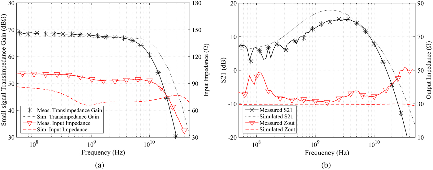
As it can be seen in Fig. 9(a), the differential transimpedance gain of the RX is 69 dz Ω over a BW of 6.2 GHz. The input impedance is around 100 Ω. A good agreement can be seen between the simulated and measured gain. However, the measured input impedance deteriorates from the simulated values since the open-loop gain of the TIA heavily depends on process variation. A higher input impedance results in the drop of BW. Further, parasitic capacitances, not included in the simulations, contribute to the decrease in BW.
Small-signal measurements of the (a) RX and (b) LDD.

Figure 9(b) shows the transfer characteristic of the LDD. A gain of 6 dB is achieved and due to a large amount of peaking, the BW is as high as 13 GHz. The high capacitance of the VCSEL is not included in these measurement and simulation results. The output impedance is maintained under 50 Ω, averaging 35 Ω, so an enhanced power transfer from the LDD to the VCSEL is possible.
Further measurements show that the OC network fulfills its purpose as the maximum output offset voltage was around 20 mV. DC voltage measurements show that the LDD has a voltage drop between VDDH and the output of around 0.45 V, thus for a VCSEL with a minimum bias of 1.8 V, a minimum VDDH of around 2.3 V would already suffice, proving the viability of the presented LDD topology.
B) Electro-optical measurements
The electro-optical frontend chip was bonded to a PCB as it can be seen in Fig. 8(a). To the input of the RX, a 25 Gbit/s PD for 850 nm light was bonded with a responsivity of 0.6 A/W and a capacitance of 140 fF. One of the DC pads can provide the anode DC voltage of 3 V. On the LDD side, a 25 Gbit/s VCSEL diode for 850 nm wavelength and 0.6 W/A slope efficiency is bonded to the chip. The bias current provided by the driver is higher than the minimum of 0.5 mA and a DC voltage higher than 1.8 V required by the VCSEL.
Figure 8(b) shows the electro-optical measurement setup. To measure the RX, a VCSEL module, biased at 10 mA, was modulated by a 27 − 1 PRBS with an amplitude of approximately 12 mA pp . Then 1 m of optical multimode fiber (MMF) was connected to the optical attenuator, which was then connected through additional 1 m of MMF to the optical probe that provided the signal to the PD. To measure the LDD, the optical probe collects the light emitted by the VCSEL and provides it to the PD module through the same 1 m MMF optical attenuator. The electrical signal of the PD module is fed to the bit error-rate tester and sampling oscilloscope.
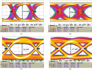
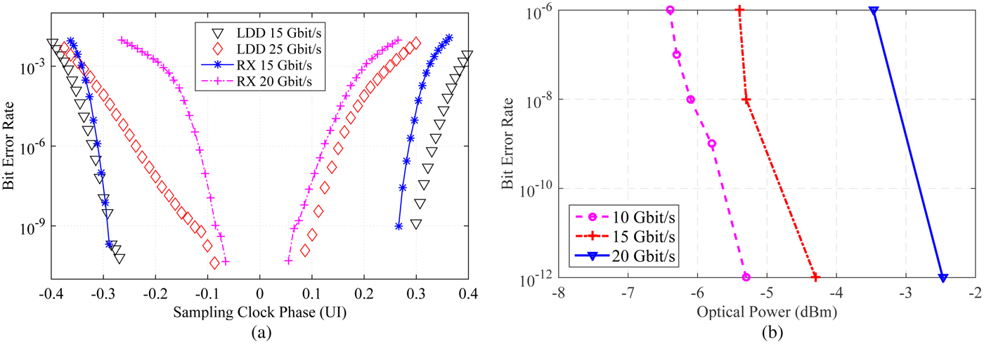
As the eye diagram in Fig. 10(b) shows, the RX works error free with a BER of 10−12 up to a DR of 20 Gbit/s. This is demonstrated also by the bathtub tests from Fig. 11(a). The single-ended output swing of the RX is approximately 175 mV pp , which is enough to drive the next block in the optical RX chain. A higher DR of 25 Gbit/s can be reached by the LDD as the eye diagram in Fig. 10(d) shows and the bathtub tests in Fig. 11(a) confirm. For this measurement, the LDD was supplied with a PRBS 231 − 1 signal with 1.3 V pp differential amplitude.
Electro-optical measurements (a, b) of the RX and (c, d) of the LDD.

Signal-integrity measurements of the electro-optical frontend. (a) Measured optical bathtub tests of the electro-optical frontend. (b) Optical sensitivity measurement of the RX.

Optical sensitivity measurements of the RX are shown in Fig. 11(b). At 20 Gbit/s, the maximum sensitivity with an error-free detection with a BER of 10−12 is −2.5 dBm. The optical modulation amplitude is estimated by measuring the average current through the PD at the DC bias pad and knowing the responsivity of the PD and modulation parameters of the VCSEL module as in [Reference Saaedi and Emami26]. At this input optical power, the transmission was error free.
Electro-optical eye diagrams of the LDD can be seen in Figs 10(c) and 10(d). The eye diagram in Fig. 10(d) and the bathtub tests in Fig. 11(a) show that the LDD is capable of driving the VCSEL up to a DR of 25 Gbit/s. Further electrical measurement shows that the driver provides a 250 mV pp voltage swing on the 50 Ω load resulting a 5 mA pp current swing through the VCSEL.
VI. CONCLUSION
An inductor-less electro-optical frontend consisting of a RX and VCSEL driver was designed in a 28 nm SLP digital CMOS process. The frontend consists of a RX with TIA, LA, output BUF, and an OC circuit in the SC technique as well as CC VCSEL diode driver, which is able to provide the high DC bias voltage. The driver has a level shifter in addition to a pre-amplifier and output stage in a floating well. Active-peaking methods are used in both of the circuits that enhance the BW and gain, thus using much less area than inductive peaking.
Small-signal S-parameter measurements show that the RX has a differential transimpedance gain of 69 dB Ω over a BW of 6.2 GHz while consuming 20 mW. An additional output BUF drives the 50 Ω instruments consuming additional 8 mW power. The LDD needs 32 mW while achieves 13 GHz BW. Commercial PD and VCSEL are bonded on a PCB to the chip. This way electro-optical measurements are performed that show the RX can work error free with a BER of 10−12 up to 20 Gbit/s with an input optical sensitivity of −2.6 dBm. The LDD can work on the other hand error free up to a DR of 25 Gbit/s.
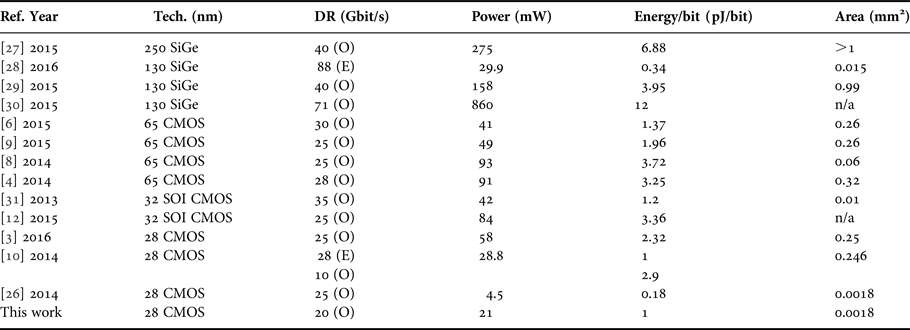
As it can be seen in Table 1, the RX is among the designs with the smallest active area and one of the most energy-efficient optical RXs. Although the BW and DR are not comparable with what can be achieved in SiGe technologies such as the designs in [Reference Schoeniger, Henker and Ellinger28, Reference Kuchta30], CMOS has the advantage of highly dense digital circuits, thus this RX can be fully integrated together with the digital core. The RX in [Reference Saaedi and Emami26] is designed in the same technology node, occupies the same area as the proposed one, but consumes less power, and it can achieve a slightly higher DR. However, a sampled system is used in the mentioned implementation, which requires four phases of precise clock. The generation of the sampling signal will occupy significant area and consume additional power resulting in comparable numbers with this design.
Comparison of the RX with state of the art

(O) Optical and (E) electrical measurement.
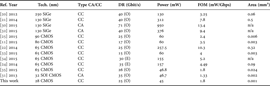
Table 2 compares the LDD from the electro-optical frontend to other recent designs. The proposed driver has the smallest area and one of the best figures of merit (FOM). The high FOM of [Reference Rylyakov31] can be attributed to the fact that it is a CA driver and thus necessitates a much lower supply voltage as the anode of the VCSEL can be separately connected to a high DC supply and driven on the cathode. It is worth mentioning that the optical measurements, in contrast with only electrical, consider also the significant power consumed by the VCSEL diode. The power consumption of the proposed driver alone is 32 mW to which 13 mW drawn by the VCSEL adds.
Comparison of the LDD with state of the art

(O) Optical and (E) electrical measurement.
With 0.003 mm2 of total active area, the electro-optical frontend is among the smallest and with a total link energy efficiency of 2.8 pJ/bit among the most energy-efficient fully integrated electro-optical frontends to date.
ACKNOWLEDGEMENTS
This work was supported in part by DFG in the framework of CRC 912 HAEC, by ESF in the framework of the Young Investigators Group Atto3D, and by the European Union's Seventh Framework Programme (FP7/2007–2013) under project ADDAPT (grant no. 619197). The authors would like to thank Gregor Tretter and David Fritsche from the Technische Universität Dresden for the assistance in preparing the layout of several components and Stefan Schumann for preparing the assembly.
 László Szilágyi is currently working toward the Ph.D. degree within the Chair for Circuit Design and Network Theory (CCN) at the Technische Universität Dresden, Germany. He received the Master of Science degree from the Carinthia University of Applied Sciences, Austria in 2012 and the Engineer degree from the Polytechnic University in Bucharest, Romania in 2010. He has received the Honorable Mention – Best Student Paper award at the IEEE-ISCAS and Cool Silicon Award. His main research interests are in the field of analog circuit design. The main focus subject is circuits for broadband and optical communications in advanced semiconductor technologies aiming for high data rates and low energy.
 Guido Belfiore received the B.Sc. degree and the M.Sc. degree in Electrical Engineering from the University of l'Aquila, Italy, in 2009 and 2012, respectively. His thesis work was on interface circuit design for resistive sensors. In 2011, he participated in an exchange program at the University of Glasgow, Scotland, UK, where he investigated the dry etch processes for high-k dielectric material layers. Since 2012, he has been with the Chair for Circuit Design and Network Theory of Technische Universität Dresden, Germany, where he is currently working toward the Ph.D. degree. His main research activities are in broadband high-speed analog driver IC design for optical components.
 Ronny Henker works as a group leader and project manager at CCN since 2011. He received the Dipl.-Ing. degree in Communications Engineering from the HfT Leipzig in 2006 and the Ph.D. degree from Dublin Institute of Technology in 2010. From 2006 to 2010, he was with the RF Institute of HfT Leipzig, where his research focused on applications of non-linear effects in optical communications. Before he joined the CCN, he was with Fraunhofer IPMS, where he worked on the characterization of MOEMS and micro-mirror arrays. His current research interests include adaptive low-power high-speed and broadband integrated circuits for optical communications.
 Frank Ellinger (S'97-M'01-SM'06) was born in Friedrichshafen, Germany, in 1972. He received the Diploma degree in Electrical Engineering from the University of Ulm, Ulm, Germany, in 1996, the MBA and the Ph.D. degrees in Electrical Engineering, and Habilitation degree in High-frequency Circuit Design from ETH Zürich (ETHZ), Zürich, Switzerland, in 2001 and 2004, respectively. Since 2006, he has been a Full Professor and Head of the Chair for Circuit Design and Network Theory, Technische Universität Dresden, Germany. From 2001 to 2006, he was Head of the RFIC Design Group, Electronics Laboratory, ETHZ, and a project leader of the IBM/ETHZ Competence Center for Advanced Silicon Electronics hosted at IBM Research, Rüschlikon, Switzerland. He has been coordinator of the projects RESOLUTION, MIMAX, DIMENSION, ADDAPT, and FLEXIBILITY funded by the European Union. He coordinates the cluster project FAST with more than 80 partners (most of them from industry) and the Priority Program FFlexCom of the German Research Foundation (DFG). Frank Ellinger has been a member of the management board of the German Excellence Cluster Cool Silicon. He has authored or co-authored over 350 refereed scientific papers, and authored the lecture book, Radio Frequency Integrated Circuits and Technologies (Springer, 2008). Professor Ellinger was an elected IEEE Microwave Theory and Techniques Society (MTT-S) Distinguished Microwave Lecturer (2009–2011). He has received several awards, including the IEEE Outstanding Young Engineer Award, the Vodafone Innovation Award, the Alcatel-Lucent Science Award, the ETH Medal, the Denzler Award, the Rohde&Schwarz/Agilent/GerotronEEEf-COM Innovation Award (twice), and the ETHZ Young Ph.D. Award.