I. INTRODUCTION
The III-nitride group of semiconductor materials is important for applications in high-frequency power electronic devices because of their wide band gap, high electron saturation velocity, and high critical electric field. Reference Eastman, Tilak, Smart, Green, Chumbers, Dimitrov, Kim, Ambacher, Weiman and Prunty1,Reference Wu, Kapolnek, Ibbetson, Parikh, Keller and Mishra2 However, high power densities also impose extreme power dissipation demands on substrates. Because of the lack of native substrates, almost all III-nitride based devices are fabricated on foreign substrates. Reference Nakamura and Krames3,Reference Nakamura, Mukai and Senoh4 Although state-of-the-art output power levels and operation frequency have been demonstrated on SiC substrates (κ = 350 W/mK), Reference Mitani, Aojima, Maekawa and Sano5,Reference Schellenberg, Kim and Phan6 power devices fabricated on less costly substrates such as Si (κ = 150 W/mK) and sapphire (κ = 40 W/mK) suffer limitations due to poor thermal conductivity of the substrates, as well as discrepancies in thermal expansion coefficient and lattice constant. Reference Gaska, Osinsky, Yang and Shur7–Reference Hirama, Taniyasu and Kasu9 Recently, there has been interest in using two-dimensional (2D) layered materials, such as graphene and BN, as template layers to assist in the heteroepitaxial growth of III-nitrides on foreign substrates by metal organic chemical vapor deposition (MOCVD). Reference Kim, Bayram, Park, Cheng, Dimitrakopoulos, Ott, Reuter, Bedell and Sadana10–Reference Kobayashi, Kumakura, Akasaka and Makimoto14 Due to weak interlayer bonding between 2D layers, they can be used as a mechanical separation layer releasing the III-nitride from the substrate. This approach allows high quality device layers to be transferred to substrates with desirable physical properties, such as high thermal conductivity polycrystalline diamond (κ = 600–2000 W/mK) or flexible polymers. As a demonstration, Hiroki et al. Reference Hiroki, Kumakura, Kobayahi, Akasaka, Makimoto and Yamamoto13 used BN grown on sapphire as a release layer to transfer an AlGaN/GaN high electron mobility transistor (HEMT) onto a copper plate, demonstrating suppression of the self-heating effect. However, to date the quality of AlGaN/GaN heterostructures grown on BN/sapphire has been inferior to GaN grown on conventional substrates.
The growth of high quality nitride layers on 2D materials is very challenging due to the lack of dangling bonds on the 2D surface. Therefore, many studies have reported employing various methods to promote nucleation, such as various buffers, Reference Chung, Lee and Yi12 functionalization methods, Reference Nepal, Wheeler, Anderson, Kub, Mastro, Myers-Ward, Qadri, Freitas, Hernandez, Nyakiti, Walton, Gaskill and Eddy11 and epitaxial graphene coated terraces. Reference Kim, Bayram, Park, Cheng, Dimitrakopoulos, Ott, Reuter, Bedell and Sadana10 An additional requirement to achieve high quality HEMT structures is to provide a high-resistivity buffer for proper channel pinch-off, low losses at high frequencies, and stable breakdown characteristics. Fe is often doped into GaN to compensate for its inherent n-type conductivity and produce a semi-insulating buffer for AlGaN/GaN-based high-performance HEMTs. Reference Cordier, Azize, Baron, Chenot, Tottereau and Massies15,Reference Wu, Leach, Ni, Li, Xie, Doğan, Özgür, Morkoça, Paskova, Preble, Evans and Lu16 Incorporating such Fe-doped GaN buffers into AlGaN/GaN HEMTs has demonstrated more stable and reproducible OFF-state breakdown characteristics for HEMTs fabricated on Si. Reference Choi, Pophristic, Cha, Peres, Spencer and Eastman17,Reference Eblabla, Li, Thayne, Wallis, Guiney and Elgaid18 However, Fe doping in MOCVD using ferrocene exhibits a long memory effect, Reference Heikman, Keller, Mates, DenBaars and Mishra19 which affects the control and reproducibility of the growth process. On the other hand, in our study of GaN grown on BN/sapphire by MOCVD, we have noticed that even unintentionally doped (undoped) GaN layers have much higher sheet resistance than when grown directly on sapphire. For these reasons, BN/sapphire is well suited as a 2D template for fabricating AlGaN/GaN based HEMTs with improved electrical properties and with the potential for transferable device layers.
In this study, we examine the characteristics of AlGaN/GaN heterostructures grown by MOCVD on BN/sapphire templates. Different nucleation procedures are evaluated based on the resulting GaN structural quality and growth characteristics. Optical and electrical qualities of the AlGaN/GaN heterostructures are also assessed using photoluminescence and temperature-dependent Hall-effect measurements. The electron mobility measured at 300 K is close to 2000 cm2/V·s with a sheet electron density of 1 × 1013 cm−2, comparable to the best obtained values in similar structures grown on conventional sapphire substrates with Fe-doped GaN buffers. Reference Cordier, Azize, Baron, Chenot, Tottereau and Massies15 The low temperature mobility measured at 10 K is as high as 33,000 cm2/V·s, consistent with the mobility that is theoretically predicted when interface roughness is the dominant scattering mechanism for the transport of 2DEG at the AlN/GaN heterointerface. We will also demonstrate the benefits of using BN/sapphire for achieving high resistivity GaN buffers without Fe doping, and show the effect on transport characteristics of the 2DEG. These characteristics correlate well with the quality of BN/sapphire template and the AlN nucleation process.
II. EXPERIMENT
For the growth experiments, we first grew few-layer sp2-bonded BN on c-plane sapphire by MOCVD using triethylboron (TEB) and NH3. Details of the BN growth process are described in our previous paper. Reference Paduano and Snure20 Since nucleation has always been a challenge in growing epitaxial GaN, which is further challenged by growing on a 2D surface, Reference AlBalushi, Miyagi, Lin, Wang, Calderin, Bhimanapati, Redwing and Robinson21 we have evaluated nucleation procedures using both low temperature (LT) GaN and AlN. The LT GaN nucleation layers were deposited at 530 °C; the high temperature AlN layers were nucleated at 1000 °C. Using H2 as a carrier gas, ammonia, trimethylaluminum (TMA), and trimethylgallium (TMG) were used as precursors for N, Al, and Ga, respectively. For Fe-doping, ferrocene was used, and kept at 20 °C. For comparison purposes, samples of the same AlGaN/GaN structure were prepared with both Fe-doped and undoped GaN buffers grown on BN/sapphire templates and directly on sapphire substrates (in this case a conventional low temperature GaN layer was used for nucleation). The AlGaN/GaN heterostructures consisted of a 2 µm GaN buffer, an undoped GaN channel, and an AlN spacer followed by an AlGaN barrier and a GaN cap. The targeted Al composition used for AlGaN barrier is 27% in this study.
The structural properties of the AlGaN/GaN multilayers were examined by x-ray diffraction using an Empyrean X'pert Pro system with a four bounce Ge (220) monochrometer. All the rocking curves of the (0002) and (
 $10\bar 12$
) diffraction peaks were recorded under symmetric or quasisymmetric ω-scan configurations using an open detector without a receiving slit. (0006) reflection was measured using ω/2θ scans to determine Al composition from the position of the AlGaN diffraction peak with respect to the diffraction peak position for GaN. A Bruker Dimension Icon AFM operating in tapping mode was used to evaluate the nucleation characteristics and surface morphology of the grown structures. Transmission electron microscopy (TEM) was used to study the interface structure between AlN/BN and AlGaN/AlN/GaN. The TEM-ready samples were prepared using the in situ FIB lift out technique on an FEI Dual Beam FIB/SEM. The samples were capped with sputtered C and e-Pt/I-Pt prior to milling. The samples were then imaged with a FEI Tecnai TF-20 FEG/TEM (FEI Company, Hillsboro, Oregon) operated at 200 kV in bright-field (BF) TEM mode, high-resolution (HR) TEM mode, and high-angle annular dark-field (HAADF) STEM mode.
The transport properties were characterized by Hall-effect measurements as temperature was varied from 10 to 300 K using a Lakeshore 7507 Hall-effect measurement system (Lake Shore Cryotronics Inc., Westerville, Ohio). The uniformities of the electrical properties, such as sheet resistance and electron mobility over a 50 mm wafer, were examined at room temperature by a Lehighton LEI-1610E contactless measurement system (Lehighton Electronics, Lehighton, Pennsylvania). The optical quality of the GaN layers are assessed by photoluminescence (PL) measurements taken at both room temperature and 10 K, using a HeCd laser at 325 nm with CW excitation and a 1-1/4 m monochrometer, all fitted to a UV-enhanced photomultiplier tube. The residual strain status in the grown structure was evaluated by Raman spectroscopy using a Renishaw inVia system with an argon laser (514 nm) excitation (Renishaw Inc., Hoffman Estates, Illinois).
III. RESULTS AND DISCUSSION
To evaluate the nucleation process for the growth of GaN on BN, several attempts were made using a LT-GaN nucleation layer (NL). However, due to the lack of dangling bonds on the sp2-bonded BN surface, most of these attempts resulted in a low density of nonuniformly distributed GaN crystalline islands, which often fail to coalesce into a continuous layer with good morphology. Occasionally, continuous layers were obtained but with relatively poor structural quality [an example is given in Fig. 1(b)]. It has been previously reported
Reference AlBalushi, Miyagi, Lin, Wang, Calderin, Bhimanapati, Redwing and Robinson21
that GaN tends to nucleate on epitaxial graphene only in highly defective regions, producing small single crystal GaN nuclei and damaging the underlying graphene. On the other hand, AlN has been found to nucleate on graphene in a polycrystalline layer, while preserving the underlying graphene layer. For growth using an AlN NL of 6–20 nm on BN/sapphire, we consistently obtained continuous layers with mirrored surface morphology. Figure 1(c) shows the FWHM values of XRD rocking curve measurements for GaN grown with different AlN NL thickness. The best FWHM values for the (0002) and (
 $10\bar 12$
) diffractions (ω-scan) are 0.13° and 0.17°, respectively [Fig. 1(a)]. These FWHM values are comparable to GaN grown on other 2D materials, as reported in the literature.
Reference Nepal, Wheeler, Anderson, Kub, Mastro, Myers-Ward, Qadri, Freitas, Hernandez, Nyakiti, Walton, Gaskill and Eddy11–Reference Kobayashi, Kumakura, Akasaka and Makimoto14
Although a thickness of 15 nm seems optimum for the AlN NL under our current process conditions, the dependence on thickness was relatively weak with high scatter [Fig. 1(c)], possibly due to variations in the BN/sapphire surface roughness. This effect will be elucidated in a future paper; instead this paper will focus on AlGaN/GaN heterostructures grown on atomically smooth BN (RMS <0.2 nm) using 9–15 nm thick AlN as the nucleation layer, since thicker AlN NLs tended to cause self-delaminating after the samples were unloaded at room temperature. The dislocation density estimated using ω-scan FWHM values
Reference Dunn and Kogh22,Reference Srikant, Speck and Clarke23
is on the order of 109 cm−2, which is higher than typical values obtained for GaN layers grown on conventional sapphire substrates. However, studies on the electron transport properties and intrinsic mobility limits of 2DEG in AlGaN/GaN
Reference Jena, Smorchkova, Elsass, Gossard and Mishra24,Reference Jena, Gossard and Mishra25
have shown that such dislocation density levels of 109 cm−2 typically do not interfere with the 2DEG, which typically has a density of 1013 cm−2. This implies that further removal of charged defects (dislocations, background impurities, etc.) would not be efficient for improving the transport mobility of the 2DEG. In fact we observed improved transport mobility in our AlGaN/GaN grown on BN/sapphire compared to the same material grown on sapphire, even though the XRD reveals more structural defects. This behavior indicates that the dislocations at the density present in our AlGaN/GaN are not the dominant scattering mechanisms limiting the transport of 2DEG. More detailed results are presented below.
XRD results for (0002) and (
 $10\bar 12$
) rocking curves obtained from GaN grown on BN/sapphire using (a) AlN nucleation layer, and (b) GaN nucleation layer. (c) FWHM of (0002) and (
 $10\bar 12$
) diffractions is given as a function of AlN NL thickness, where dash lines are a guide for the eye only.

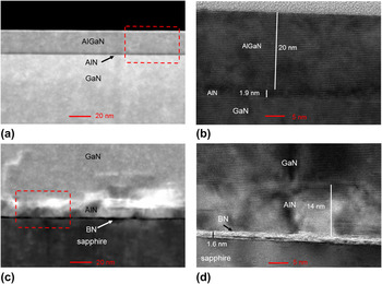
Cross-sectional TEM was performed on the AlGaN/GaN heterostructure grown on BN/Sapphire to evaluate the interfaces between the AlN NL, BN, and GaN. Figure 2(a) shows a high-angle annular dark-field (HAADF) image of sample A, exhibiting the final AlGaN/GaN heterostructure grown on BN/sapphire. (Note that the interface region of BN/sapphire interface is not shown in this figure.) The corresponding high resolution (HR) TEM image of the HEMT region is shown in Fig. 2(b). The AlGaN/AlN/GaN stack shows a very uniform, smooth, and high quality interface between these layers, which is barely distinguishable without reference to the Z-contrast in the HAADF images. The interface region of the AlN/BN/sapphire is shown in Fig. 2(c) as a HAADF image, where the presence of a BN spacer (the dark region) can be observed between AlN and sapphire substrate. The corresponding HR-TEM image of the few-layer BN and AlN nucleation layer is shown in Fig. 2(d), where a layered structure parallel to the c-plane sapphire can be identified, this corresponds to BN with a thickness of ∼1.6 nm. The thickness of AlN nucleation layer is estimated to be ∼14 nm. The HR-TEM results confirm that (i) AlN nucleates from the surface of BN but not from the sapphire substrate; (ii) the AlN nucleation layer is oriented along [0002] direction with lattice plane spacing of ∼0.5 nm, and (iii) the few-layer BN film is well preserved after GaN growth. Compared to the results of using 2D graphene templates in previous III-N MOCVD growth, Reference Nepal, Wheeler, Anderson, Kub, Mastro, Myers-Ward, Qadri, Freitas, Hernandez, Nyakiti, Walton, Gaskill and Eddy11,Reference AlBalushi, Miyagi, Lin, Wang, Calderin, Bhimanapati, Redwing and Robinson21 it is not surprising to see well-preserved 2D BN, since BN is very stable under MOCVD growth conditions.
Cross section TEM (a) image taken under HAADF STEM mode near top surface of AlGaN/AlN/GaN structure; (b) HR-TEM image showing GaN/AlN insertion layer and AlGaN barrier; (c) HAADF image of GaN/AlN/BN/sapphire interface, where a BN spacer is clearly shown; (d) HR-TEM showing layered BN with thickness ∼1.6 nm and well-oriented AlN nucleation layer ∼14 nm.
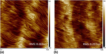
AFM measurements were carried out to examine the surface morphology of the AlGaN/GaN heterostructures. Figure 3 compares the AFM image of a typical surface of AlGaN/GaN grown on BN/sapphire and the same structure grown on sapphire. The root mean square of roughness (RMS) was 0.283 nm for AlGaN/GaN grown on BN, compared to 0.257 nm on sapphire. The undulation exhibited in the AFM images is very similar to the GaN surface morphology commonly observed on sapphire substrates. We also observed some increase in RMS roughness when we use relatively rough BN/sapphire templates, consistent with the known sensitivity of BN surface morphology to various process conditions. Reference Paduano, Snure and Shoaf26,Reference Snure, Paduano and Kiefer27 For BN surface RMS roughness up to 1 nm, relatively smooth AlGaN/GaN surface (RMS ∼ 0.314 nm) can still be obtained. However, increased roughness of the BN/sapphire template did show significant effect on the crystalline quality of the GaN layer as revealed by XRD. When Fe doping was introduced in the GaN buffer, we did not observe a notable change in surface morphology.
AFM images of AlGaN/GaN surface morphology (a) grown on BN/sapphire, and (b) grown on sapphire, with a root mean square roughness indicated on each image.

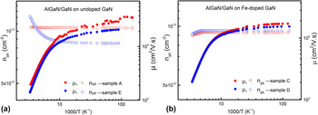
To evaluate the quality of the AlGaN/GaN heterostuctures, the mobility of the 2DEG was assessed. Hall-effect measurements were carried out as a function of temperature in the 10–300 K range at a fixed magnetic field. Figure 4 depicts the temperature dependence of electron mobility (µ) and sheet electron density (n sh) for AlGaN/GaN grown on BN/sapphire and sapphire substrates using (a) an undoped GaN buffer and (b) an Fe doped GaN buffer. Measured values of µ for different samples at 10 and 300 K are summarized in Table I, along with the corresponding n sh, average sheet resistance (R sh at 300 K), and the XRD results discussed above. The electrical properties from similar structures grown on SiC and sapphire are included for comparison. Figure 4 clearly exhibits near-constant carrier density over the entire temperature range for samples C and D (Fe doped buffer grown on BN/sapphire and sapphire), and for sample A (undoped GaN buffer grown on BN/sapphire). When the undoped GaN was grown directly on the sapphire without the BN (sample E), the apparent sheet carrier density increased with increasing temperature [Fig. 4(a)]. This behavior is commonly seen on sapphire substrates, Reference Smorchkova, Keller, Heikman, Elsass, Heying, Fini, Speck and Mishra28 because undoped GaN grown on sapphire is typically n-type with a background carrier concentration of ∼2 × 1016 cm−3, possibly due to residual oxygen impurity from the substrate. In this scenario, the bulk carrier density in the GaN buffer increases with temperature due to thermal activation. Since the carrier density of the 2DEG (n 2d) is independent of temperature, we can differentiate the contribution of the buffer from that of the 2DEG by comparing the temperature dependences of n sh in the various samples (Fig. 4). The constant n sh in samples C and D confirms that parallel conduction is negligible in the GaN buffer (n sh = n 2d) due to Fe-related compensation, whereas the increasing sheet carrier density with temperature in sample E is clearly due to the conductive buffer. However, sample A grown on BN/sapphire showed no change in sheet carrier density with increasing temperature, indicating negligible parallel conduction in the buffer even without Fe doping, which is similar to the behavior of high resistivity GaN grown on SiC substrates. The sheet resistance across the 2-in wafer (shown in Table I) also showed much better uniformity when the nonuniform buffer conduction is reduced.
Sheet carrier density and Hall mobility as a function of temperature for AlGaN/GaN heterostructures (a) grown on undoped GaN buffer, and (b) grown on Fe doped GaN buffer, where red symbols are for sapphire substrates, and blue symbols are for BN/sapphire templates.

Summary of XRD and Hall-effect measurement results for samples in this study.

a BN was deposited at low N/B ratio, see discussion.
For AlGaN/GaN heterostructures grown on a conductive GaN buffer (samples E and F), the overall mobility is affected by the 3D transport in the parallel conducting buffer, especially at room temperature; therefore, the measured mobility is lower than the pure 2DEG mobility. Reference Jena, Smorchkova, Elsass, Gossard and Mishra24,Reference Lisesivdin, Yildiz, Balkan, Kasap, Ozcelik and Ozbay29 In this regard, AlGaN/GaN grown on BN/sapphire, benefiting from the highly resistive GaN buffer, exhibited improved µ300 K. However, this improvement due to the template can be significantly affected by the quality of the BN. We observed different magnitudes of sheet carrier density increase depending on the quality of the BN. As an example given in Table I, sample B is grown in the same run as sample A. The difference between sample A and B is that the BN layers were deposited under different V/III ratios—2700 and 900, respectively. As shown in our previous paper, Reference Paduano, Snure and Shoaf26,Reference Snure, Paduano and Kiefer27 the morphology of these BN layers is sensitive to the growth conditions. At a high V/III ratio, growth of BN exhibits a self-terminating mode of growth, resulting in a BN layer with an atomically smooth surface. At a V/III ratio of 900; however, the BN layer is highly defective with a high density of holes. Reference Snure, Paduano and Kiefer27 The lower value of µ300 K in sample B is consistent with the existence of transport contributions from both 2DEG and a parallel channel. Therefore, good quality BN is critical to effectively reduce parallel conduction in the GaN buffer.
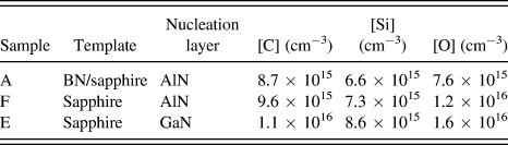
To further confirm the effect of BN on the residual donor impurities in the GaN buffer, SIMS analyses were performed on samples A, E, and F for [O], [C], and [Si]. (There was no intentional Fe doping in theses samples.) Results are summarized in Table II, where the background impurity levels are derived from SIMS profile near the center of the GaN buffer (∼1 µm below surface) using a 50-point average. We see that [Si] is the lowest in all three samples (close to the SIMS detection limit); [C] has a very similar level of ∼1 × 1016 cm−3; and [O] exhibits some variation between the samples. The lowest [O] level was detected in sample A, consistent with its lowest residual donor level in the GaN buffer (as obtained from Hall measurements, Table I). Slightly reduced buffer conductivity in sample F (compared to sample E) is also consistent with a reduced [O] background.
Summary of SIMS results on background impurity concentrations (average over 50 points at ∼1 μm below surface).

We should note that the residual donor concentration obtained from Hall measurements may not always be in good agreement with SIMS results. This is because SIMS measurements are not always accurate at concentrations near the detection limit, and also some of the impurities may be electrically inactive. Reference Look, Fang and Claflin30 Nevertheless, the differences in measured oxygen concentration are noticeable, especially near the substrate interface.
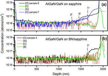
Figure 5 shows the SIMS profiles from samples A, E, and F [where the background [C] and [Si] profiles are shown for only one of the samples on sapphire substrates in Fig. 5(a)]. [O] exhibits an abnormal increase in all three samples at ∼250–400 nm before the substrate interface, as indicated by marker lines 1 and 2 in the figure. This increase in [O] is consistent with our previous SIMS measurements on films grown on sapphire, and is accompanied by a similar increase in [Al]. It was suggested that during SIMS data acquisition, preferential sputtering in the local area around core of screw dislocations can be responsible for causing long “tunnels” reaching the sapphire substrate. Reference Kim and Andersson31 A related observation is that the distance from the substrate interface at which the abnormal increase occurs corresponds well with the thickness at which the initial growth of GaN becomes fully coalescent. Regardless, the abnormal [O] profile renders the effect of oxygen diffusion near the substrate interface nearly unobservable. We can however see that [O] exhibits a longer “tail” (out to ∼400 nm) in samples E and F (marker line 3 in Fig. 5(a) indicates where [O] approaches the background level in both of these samples), compared to the arguably much sharper change in sample A [in Fig. 5(b), [O] reaches the background level near marker line 1]. This indicates that the out-diffusion of oxygen from the substrate is reduced due to BN, which is consistent with the lowest [O] background and the highest resistivity of the GaN buffer in sample A. These results clearly suggest that a good quality BN plays an important role in effectively reducing residual donor impurities in GaN.
SIMS profiles for background impurities [O], [C], and [Si] in (a) GaN grown on sapphire substrates with GaN and AlN as nucleation layers, where only one [C] and [Si] profiles were shown; (b) GaN grown on BN/sapphire, where [B] is also shown as a marker for substrate interface. Marker lines: 1 indicates the point at which the abnormal increase of [O] occurs for AlN NL; 2 indicates the same for GaN NL; and 3 indicates where the [O] approaches the background level in both samples E and F.

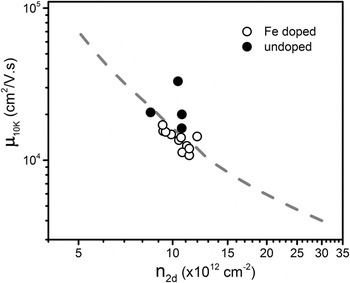
When the 3D bulk conduction in the GaN buffer ‘freezes out’ at low temperature, the measured Hall mobility at 10 K (µ10 K) represents the transport of the 2DEG alone. For a simple relation µ i = eτ i /m*, where τ i is a relaxation time (or 1/τ i is scattering rate) for a process i, Matheissen's rule provides a way to combine the effect of the different scattering processes, assuming they act independently. We found that the typical µ10 K values of our samples (from 15,000 to 33,000 cm2/V·s with n 2d ∼1 × 1013 cm−2) are in the range where the dominant scattering mechanism limiting µ10 K is interfacial roughness between the GaN and the AlN insertion layer. The scattering rate associated with such interfacial roughness (1/τir) has been treated by Jena et al. Reference Jena, Smorchkova, Elsass, Gossard and Mishra24 for AlGaN/GaN, which correlates µ with n 2d for a given interface roughness (characterized by root mean square roughness height and correlation length). In Fig. 6, a dashed-line depicts this characteristic dependence of µ on n 2d described in Ref. Reference Jena, Smorchkova, Elsass, Gossard and Mishra24, and µ10 K values obtained in this work are plotted as a function of n 2d. Good agreement is seen between experimental µ10 K values and the predicted characteristic of mobility under the limit of interface roughness scattering. Scatter can be attributed to variations in interface roughness. The highest values of µ10 K are associated with undoped GaN buffer, as shown in solid symbols in Fig. 6. Additionally, the quality of the BN can affect the AlGaN/GaN in many ways. As discussed before, we observed little dependence of crystalline quality on the AlN NL thickness [Fig. 1(c)], whereas the BN quality has shown a significant impact. The effect of the BN layer quality was also observed in the 2DEG mobility at low temperature, showing a correlation with BN roughness. In this regard, optimization of the BN layer is likely as important as optimization of the AlN NL. A systematic study is underway to understand the effect of the BN layer on the quality of the subsequent III-nitride.
Low temperature mobility (10 K) is plotted as a function of 2D sheet carrier density, where open circles are for samples grown on Fe-doped GaN buffer and solid symbols are for samples grown on undoped GaN buffer, and dashed-line depicts calculated dependence Reference Jena, Smorchkova, Elsass, Gossard and Mishra24 for a given interface roughness with RMS roughness of 0.2 nm and correlation length of 1 nm.

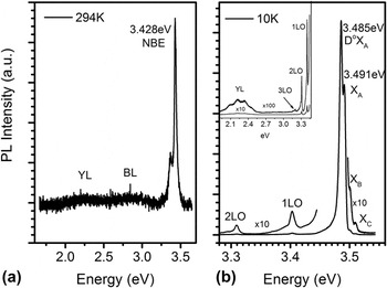
To further assess the quality of the GaN/BN layer, PL measurements were performed at room temperature, as well as at 10 K. Figure 7(a) shows the PL spectrum obtained at room temperature. A strong near-band-edge (NBE) emission was observed at 3.43 eV, while defect-related yellow band (at ∼2.5 eV) and blue band (at ∼2.9 eV) emissions Reference Reshchilov and Morkoc32 were barely noticeable. In Fig. 7(b), the PL spectrum recorded at 10 K exhibits two strong emissions at 3.485 and 3.491 eV, corresponding to neutral-donor-bound-exciton (DoXA) and free-exciton (XA) transitions, respectively. Reference Viswanath, Lee, Yu, Kim, Choi and Hong33 On the high energy side of the spectrum, emissions due to free-excitons XB and XC were also visible on the expanded scale. The free-exciton transition energies are close to the reported values in undoped GaN grown on sapphire by MOCVD. Reference Kim and Andersson31 On the low energy side of the spectrum, a few LO phonon replicas at energy separations that are multiples of ∼91 meV are visible, with decreasing intensity as the order increases. An emission corresponding to donor acceptor pair (DAP) transition, typically observed at ∼3.27 eV, Reference Reshchilov and Morkoc32 is not detectable in our GaN grown on BN/sapphire. A very weak and broad emission peak is observed in the range of 2–2.5 eV, corresponding to the defect-related yellow luminescence, Reference Reshchilov and Morkoc32 shown in the insert of the Fig. 7(b) with an expanded scale. Overall, the PL indicates the GaN grown on BN/sapphire is of good optical quality.
(a) PL spectrum recorded at room temperature, where YL and BL indicate the positions of yellow band and blue band emissions commonly observed near 2.25 and 2.9 eV respectively. Reference Reshchilov and Morkoc32 (b) PL spectrum measured at 10 K. Inset shows yellow band with an expanded scale.

Residual strain in the heterostructure is another important issue affecting device performance, which can be addressed by growing on a 2D BN template. To estimate the residual strain in GaN grown on BN/sapphire, Raman spectroscopy was performed at room temperature on samples grown on BN/sapphire and compared with layers grown on SiC and sapphire substrates. It is known that biaxial strain in c-plane can be well-represented by the frequency shift of the E2 high (
 ${\rm{E}}_2^{\rm{H}}$
) mode in GaN.
Reference Zhao, Xu, Xie and Tong34–Reference Kitamura, Nakashima, Nakamura, Furuta and Okumura36
Figure 8 shows the
 ${\rm{E}}_2^{\rm{H}}$
mode measured on four samples. For comparison, we adopted the value of 567.6 cm−1 for the
 ${\rm{E}}_2^{\rm{H}}$
mode phonon frequency in “stress-free” GaN from the literature.
Reference Harima37
A blue shift of the
 ${\rm{E}}_2^{\rm{H}}$
peak by 2 cm−1 can be seen in GaN on sapphire, while a red shift of less than 1 cm−1 is seen for GaN grown on SiC. Consistent with the findings reported in the literature, the GaN layer grown on a sapphire substrate with a LT-GaN NL is under compressive stress, while the GaN grown on SiC with an AlN NL is under tensile stress. For samples grown on BN/sapphire, a shift similar to that of GaN grown on sapphire was observed in Fig. 8, indicting a similar degree of compressive stress in the GaN. However, the spectrum collected on the same GaN layer after release from the substrate showed an
 ${\rm{E}}_2^{\rm{H}}$
peak close to 568 cm−1, indicating stress relaxation. Using the
 ${\rm{E}}_2^{\rm{H}}$
frequency change with respect to “strain free” value, Δω (cm−1) = Cσ
xx
, where C is the linear stress coefficient, we can estimate biaxial stress (σ
xx
) in each sample (results given in Table III). Since experimental values for stress coefficients in the literature are scattered due to the different methods by which biaxial stress is evaluated,
Reference Harima37
we adopt an experimental value of 2.9 cm−1/GPa, which is in better agreement with a theoretical value (2.4 cm−1/GPa) calculated using first-principles.
Reference Wagner and Bechstedt38
Estimated stress values given in Table III are an average over multiple (25) spectra collected at the same location for each sample, where the
 ${\rm{E}}_2^{\rm{H}}$
peak frequency in each spectrum was obtained through curve fitting rather than from the measured raw data. The standard deviation (STD) represents the variation in stress among the 25 spectra analyzed. It is seen that GaN layer grown on BN/sapphire remains compressively stressed until the layer is released from the substrate, consistent with a previous report
Reference Kobayashi, Kumakura, Akasaka and Makimoto14
for GaN grown on BN. Comparing the residual stress in GaN before and after it is released from the substrate, we also notice that the stress represented by the shift of the
 ${\rm{E}}_2^{\rm{H}}$
peak frequency is well correlated with a shift of the NBE peak (∼8 meV) observed in the room-temperature PL spectrum. On a released GaN film, Raman measurements were performed to check the sp2-bonded BN on the backside of the GaN film and on the substrate surface. The signature Raman shift for sp2-bonded BN was observed on both sides at ∼1370 cm−1, indicating that the bonding between the 3D and the 2D surfaces (i.e., substrate/BN or GaN/BN) is stronger than the pure van de Waals bonding between adjacent BN layers.
Raman spectra collected at 300 K showing the
 ${\rm{E}}_2^{\rm{H}}$
mode from GaN layers grown on sapphire, SiC, BN/sapphire, and released from BN/sapphire, as indicated. The black vertical dashed line at ω = 567.6 cm−1 represents
 ${\rm{E}}_2^{\rm{H}}$
mode phonon frequency in “stress free” GaN.
Reference Harima37

Biaxial stress in GaN grown on different substrates calculated from
 ${\rm{E}}_2^{\rm{H}}$
peak shift with respect to
 ${\rm{E}}_2^{\rm{H}}$
peak frequency of 567.6 cm−1 in stress-free GaN.
Reference Zang and Chua35
(STD represents the variation in stress; NBE is from room temperature PL).

IV. CONCLUSION
AlGaN/GaN heterostructures were grown by MOCVD on sp2-bonded BN using AlN as a nucleation layer. XRD rocking curve measurements indicate structural quality, with FWHMs of 0.13° and 0.17° for (0002) and (
 $10\bar 12$
) diffraction peaks, respectively. Cross sectional TEM confirms that the BN is preserved under the AlGaN/GaN structure. AFM images show that the AlGaN/GaN surface morphology is smooth with RMS roughness comparable to that of GaN grown on sapphire substrates. The transport characteristics showed improved GaN buffer resistivity, with electron mobility at 300 K close to 2000 cm2/V·s and a sheet electron density of 1 × 1013 cm−2, values comparable to the best obtained on similar structures grown on conventional sapphire substrates with Fe doped GaN buffers. Good quality BN on sapphire was found to be effective for reducing residual donor impurities in the GaN buffer. PL measurement reveals very weak defect-related emissions, indicating good optical quality of the GaN/BN/sapphire structures. The residual strain in GaN grown on BN/sapphire is found to be compressive, and is nearly eliminated when the GaN layer is released from the substrate.
ACKNOWLEDGMENTS
Authors would like to thank B. Moore and T. Prusnick for providing assistance in Raman measurements and strain analysis. Authors would also like to thank W. Rice and T. Cooper for the assistance in PL and transport measurements. This work is funded by Air Force Office of Scientific Research under task number 16RYCOR331. This support is gratefully acknowledged.