I. INTRODUCTION
Microwave power transfer (MPT) technology has been investigated since the 1960s. Recently, many MPT systems have been proposed, such as ultra-long-range wireless power transfer for space solar-power satellite and wireless power supplies for sensor networks, electric vehicles, and mobile phones [Reference Takano1–Reference Yoshida, Hasegawa and Kawasaki3]. Most of these studies have been based on a microwave beam forming by array-antenna techniques. The recent advances in MPT are closely tied with these of antenna and radio frequency (RF) power semiconductor technologies.
The RF GaN amplifier serves an important role in MPT transmission system. The GaN semiconductor offers a wider band gap than those mode of Si or GaAs, and faster electron mobility than those mode of SiC. Hence, GaN semiconductor techniques are necessary to meet the demands of next-generation high-power RF systems. Recently, high-power and high-efficiency GaN amplifiers have been developed [Reference Kanto, Satomi, Asahi, Kashiwabara, Matsushita and Takagi4–Reference Stameroff, Ta, Pham and Leoni16]. For instance, Kuroda et al. reported a high-efficiency C-band (5.8 GHz) GaN amplifier with 71.4% power-added efficiency (PAE) in 2010 [Reference Kuroda, Ishikawa and Honjo17]. In addition, Kobayashi et al. reported a high-power S-band (2.1 GHz) GaN solid-state power amplifier with kW-class power output in 2013 [Reference Kobayashi, Yoshida, Yamamoto and Kawasaki18]. The transmitted power and efficiency are directly affected by the operating power and the DC–RF conversion efficiency of the GaN amplifier. Therefore, these novel GaN amplifiers are extremely useful for high-power and high-efficiency MPT systems.
Recently developed long-range MPT systems conventionally use array-antenna techniques for controlling the microwave beam. In the MPT system, the beam control techniques are critically necessary to improve the transmission efficiency and to reduce the level of the sidelobes. In 2015, Ishikawa and Shinohara reported the formation of a flat-topped beam by implementing phase tuning for each antenna, and this was used in an MPT system installed on a vehicle roof [Reference Ishikawa and Shinohara2].
Sidelobe-reduction techniques have also been studied in the context of passive antenna design in conventional studies. In general, the operated RF power is larger than the microwave power required for communication. MPT systems must not interfere with traditional wireless communication or affect the immediate environment. Hence, it is desirable to reduce the level of the sidelobes derived from the array antenna. Low-sidelobe antenna techniques with element phase control have been reported [Reference Goto and Tsunoda19–Reference Zainal, Kamarudin, Yamada, Seman, Khalily and Jusoh24]. In addition, sidelobe reduction by amplitude control has been investigated [Reference Huang, Zhou, Chio, Hui and Yeo25, Reference Nikkhah, Mohassel and Kishk26]. For instance, Chen et al. proposed a low-sidelobe array antenna with a filtering microstrip antenna in 2017 [Reference Chen, Hu, Li, Chu and Lancaster27]. In these conventional designs, the sidelobe is mainly reduced using non-uniform division techniques.
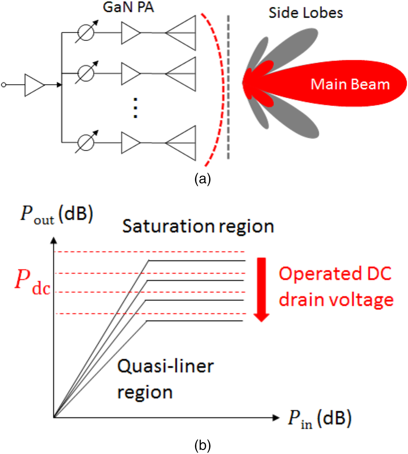
It is difficult to tunable control the sidelobe level via the conventional circuit approach. However, situationally tunable sidelobe control is required for MPT systems developed for EVs, mobile phones, and wireless sensors. In long-range MPT systems, active-array antennas are generally used. In this study, the active-array antenna configuration consisting of antenna elements with GaN power amplifiers, as shown in Fig. 1(a), is assumed. In conventional studies, sidelobe reduction by an effectual amplitude distribution on the surface of antenna was reported by Taylor in 1955 [Reference Taylor28]. In this work, sidelobe reduction was achieved using GaN active-antenna techniques. The input–output characteristics of an amplifier are shown in Fig. 1(b). In general, it is possible to control the saturated power output of the amplifier by adjusting the operating drain DC power level. In this work, the saturated output power of GaN amplifiers is controlled to realize sidelobe reduction. The advantage of this sidelobe reduction method based on an active-antenna approach is that it is possible to tune the sidelobes by adjusting the operating DC power of the amplifier.
Low-sidelobe active-array antenna: (a) active array antenna configuration and (b) amplifier input–output characteristics for various operating DC drain voltages.
In this study, a tunable sidelobe reduction technique with a GaN active-array antenna is proposed. First, a single-stage GaN amplifier is designed and fabricated. Second, a four-way GaN active-array antenna is designed and fabricated. Then, the resulting low-sidelobe active antenna is characterized.
II. AMPLIFIER DESIGN AND FABRICATION
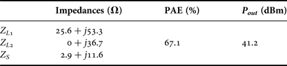
In this study, a power GaN HEMT (Sumitomo Elec, SG0601C) is used for the amplifier design. The load- and source-side input impedances of the chip are determined via a load-pull simulation with a non-linear model using Kesignt ADS, as shown in Table 1. In Table 1, Z L1 and Z L2 are the load-side input impedances at the 5.8 GHz fundamental frequency and the 11.6 GHz second harmonic frequency, respectively. Z S is the source-side input impedance at the fundamental frequency. In this simulation, the input RF power, P in , the gate DC voltage, V g , and the drain DC voltage, V d , are 30 dBm, −2.5, and 50 V, respectively. Under these impedance conditions, a 67.1% PAE and a 41.2 dBm RF output power (P out ) are calculated by the simulation. Hence, in the following amplifier design, these conditions are targeted for the amplifier circuits.
Calculated load-pull impedances at the fundamental and second harmonic frequencies with 30 dBm RF input.

A) Single-stage amplifier
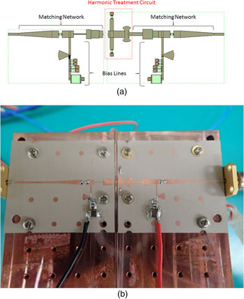
First, the single-stage GaN amplifier is designed and fabricated. The designed GaN amplifier consists of matching networks, bias lines, and a harmonic treatment circuit as shown in Fig. 2(a). The DC cut capacitors are mounted in the matching network and the bypass capacitors are mounted in the bias lines. The harmonic circuit, which is designed with short stabs, as shown in Fig. 2(a), treats a second harmonic. These circuits are fabricated on a dielectric substrate of Arlon AD1000 (with ɛ r = 10.2, tanδ = 0.0023, and thickness of 0.8 mm). The load- and source-side input impedances of the designed circuit are Z L1 = 28.2 + j53.6 Ω, Z L2 = 5.8 + j35.4 Ω, and Z S = 6.5 + j10.1 Ω. The single-stage GaN amplifier is fabricated as shown in Fig. 2(b). The GaN HEMT chip is mounted on a copper plate, which is connected to the circuits by wires. The circuit substrates are also mounted on the copper plate.
(a) Designed GaN amplifier layout and (b) image of the fabricated amplifier.

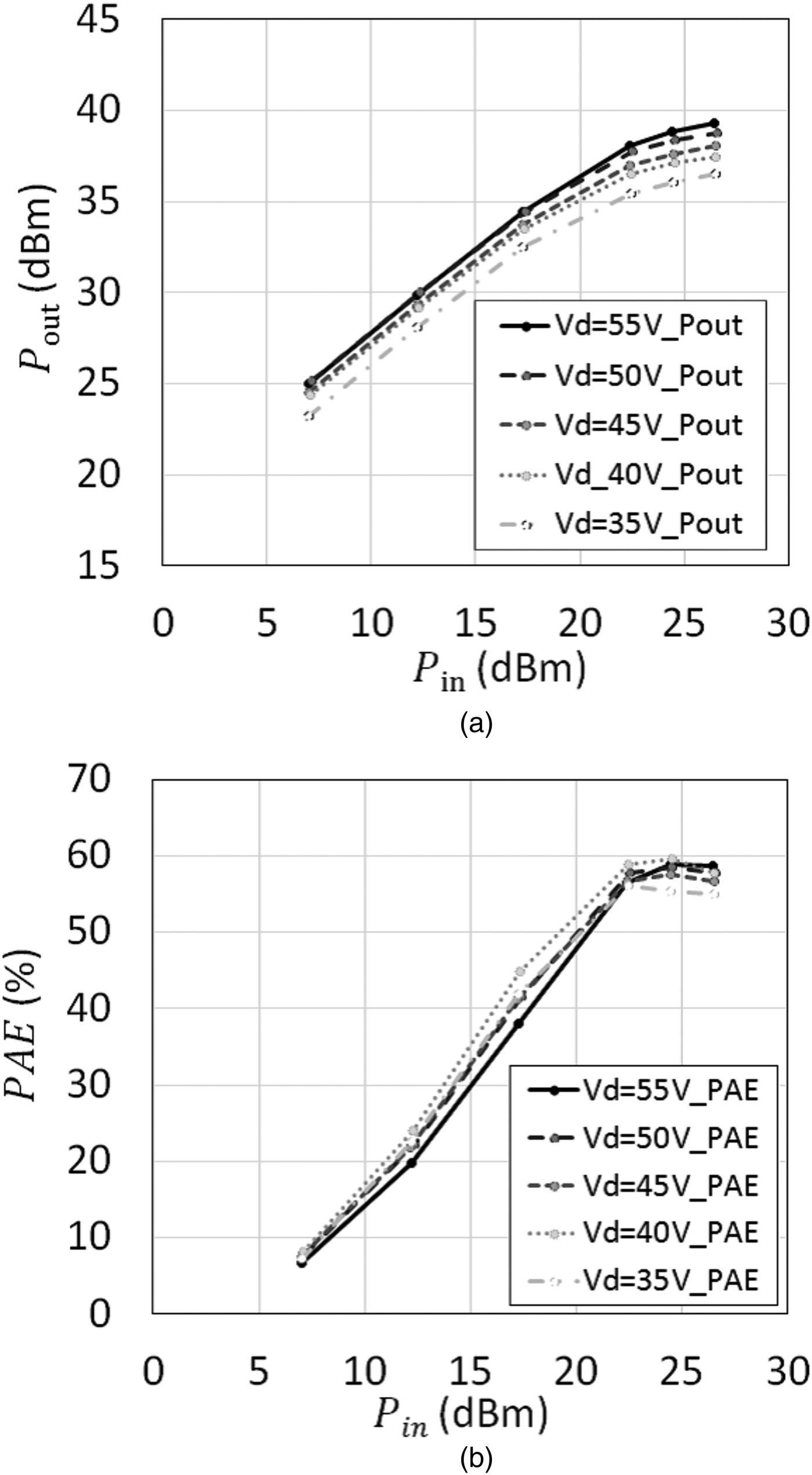
The measured input–output characteristics are shown in Fig. 3. In Figs 3(a) and 3(b), the effects of the drain voltage levels on the output power, P out , and on the PAE are illustrated. According to Fig. 3(a), the maximum output power is 39.3 dBm when V d = 40 V, which decreases to 36.5 dBm when the drain voltage level is reduced to V d = 35 V. In contrast, the maximum PAE peaks at 59.6% when V d = 40 V, P in = 24.5 dBm. In each drain voltage condition tested, maximum PAEs over 50% are confirmed. According to the results, the amplifier output power can be controlled between 36.5 and 39.3 dBm with minimal reduction in the PAE, which facilitates sidelobe reduction in the GaN active-array antenna.
Measured input–output characteristics at operating the DC drain voltage between 35 and 55 V: (a) measured output power P out and (b) measured PAE.

B) Four-way amplifier
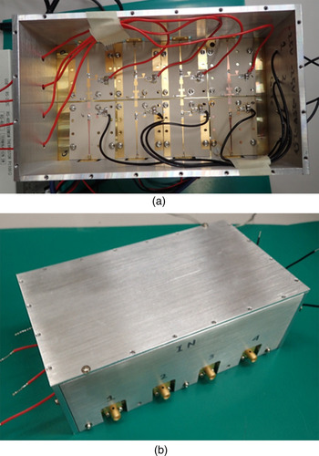
In this study, the sidelobe reduction is based on a four-way GaN active-array antenna. Hence, a four-way amplifier is designed and fabricated, as shown in Fig. 4. The fabricated amplifier circuits are mounted to a copper plate and packed in an aluminum case of 90 mm width, 162 mm length, and 58 mm height.
Fabricated four-way GaN amplifier.

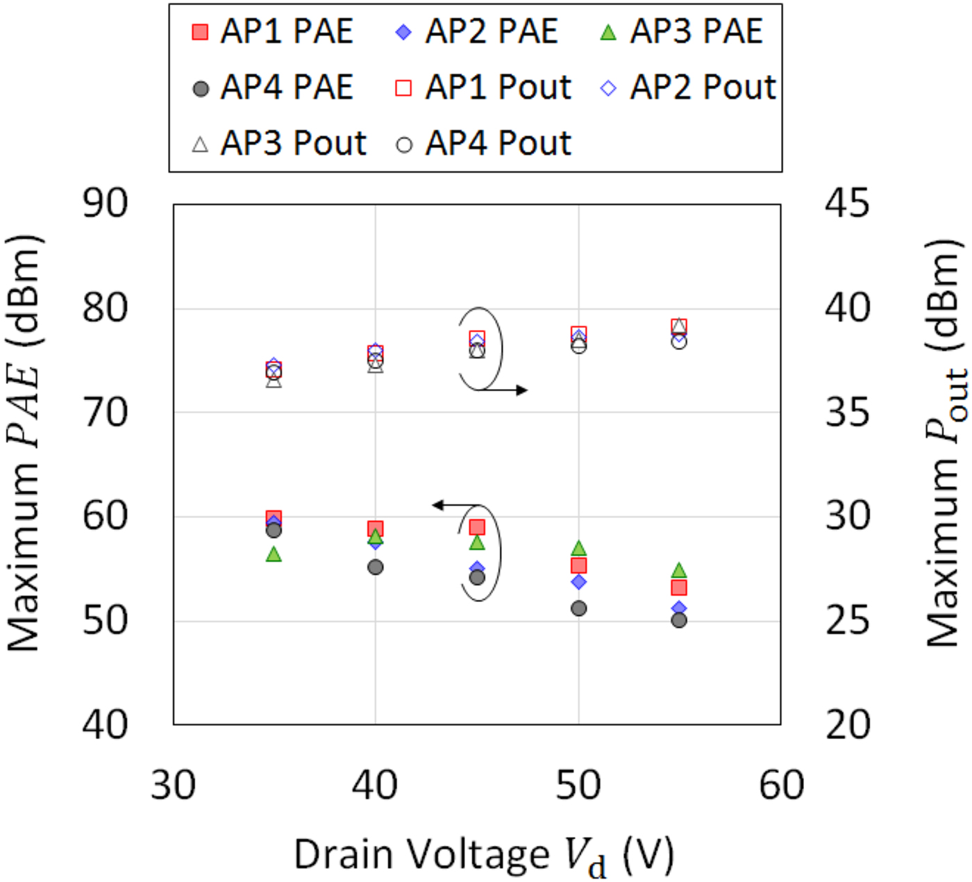
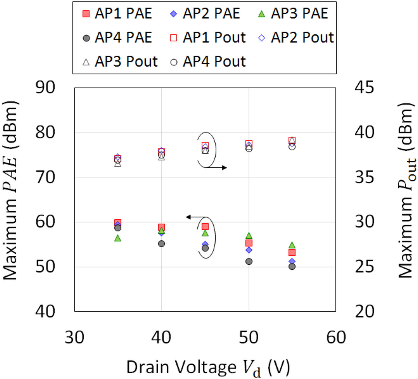
The measured maximum PAE and P out under difference applied drain voltages are illustrated in Fig. 5. In these measurements, the maximum input power is 25.36 dBm. The measured maximum output power increases as the drain voltage increases. On the other hand, the measured PAE decreases with increasing drain voltage, reaching a minimum of 50.1% when the drain voltage is 55 V. However, the PAE remains within a range of 50–60% for all drain voltages tested.
Measured maximum PAE and P out as a function of the drain voltage.
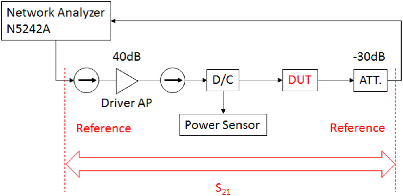
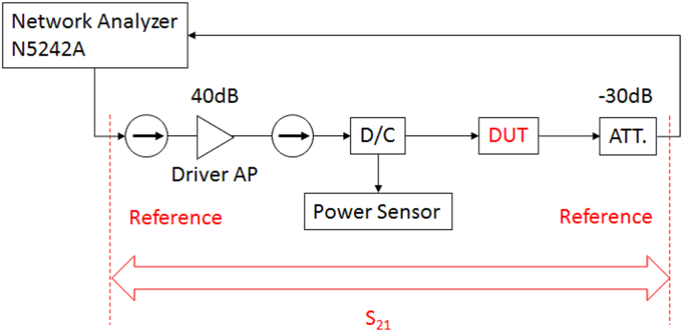
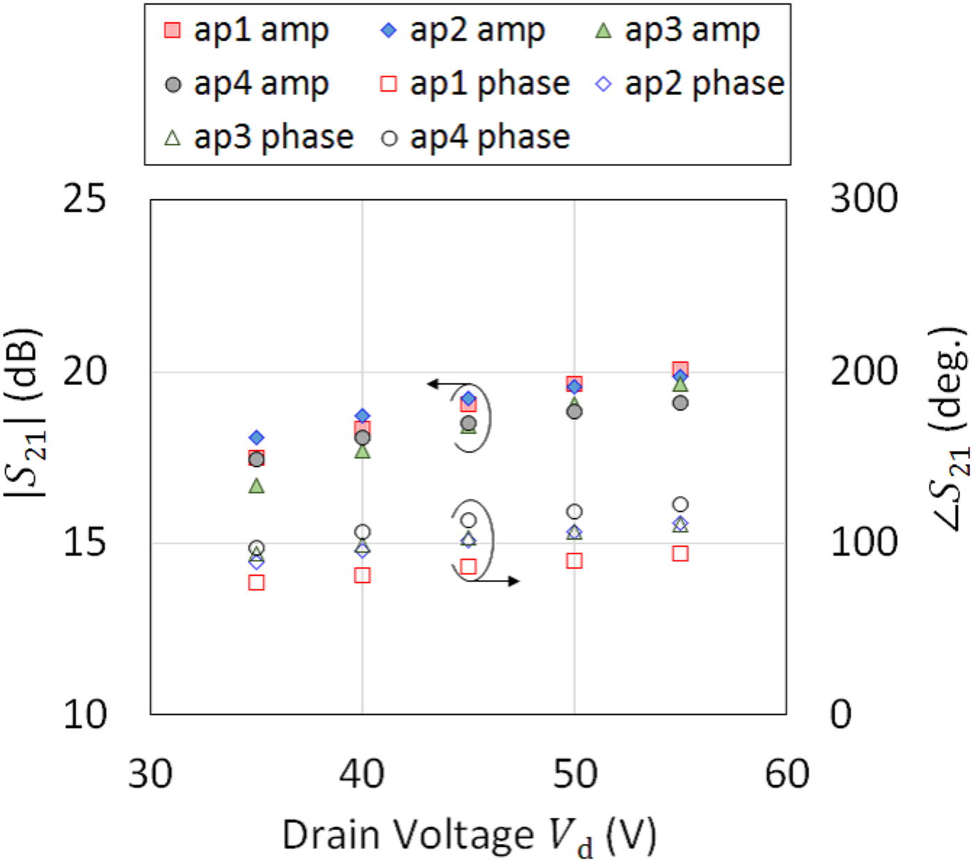
The factors affecting the input–output characteristics, such as the maximum PAE and output power, are measured. However, the output phase of the amplifier may be shifted for each drain voltage. Therefore, the GaN amplifier is measured using a system comprising of a vector network analyzer, a driver amplifier, and other RF components as shown in Fig. 6. Using this system, the S-parameters of the amplifier, including the isolators, the 40 dB driver amplifier, the directional coupler, and the 30 dB attenuator, are measured. The amplitude and phase compositions of the S-parameters include the independent characteristics of these components. However, the effect of the drain voltage on the fabricated GaN amplifier, which hardly depends on the component characteristics, is also considered using this measurement system.
Measurement system for S-parameters of GaN amplifier under high-power conditions using a network analyzer.
III. LOW-SIDELOBE ANTENNA DESIGN
The 1 × 4 array antenna with a circular patch antenna, shown in Fig. 7(a), is designed and fabricated. A high-frequency three-dimensional EM field simulator (CST Microwave Office) is used in this design. This antenna is fabricated on a dielectric Nippon Piller Packing NPC-F260A (ɛ r = 2.55, tanδ = 0.0018, and thickness of 1.6 mm) substrate. The diameter of the patch antenna is 17.4 mm and the feed pin is shifted 2.7 mm from the center. The calculated and measured values of the reflection coefficient |S 11|s are illustrated in Fig. 7(b). Both theoretical and experimental results show that |S 11| is reduced to <−10 dB at 5.8 GHz.
Designed 1 × 4 array antenna: (a) antenna layout and (b) measured and calculated values of the antenna reflection coefficient |S 11|s.

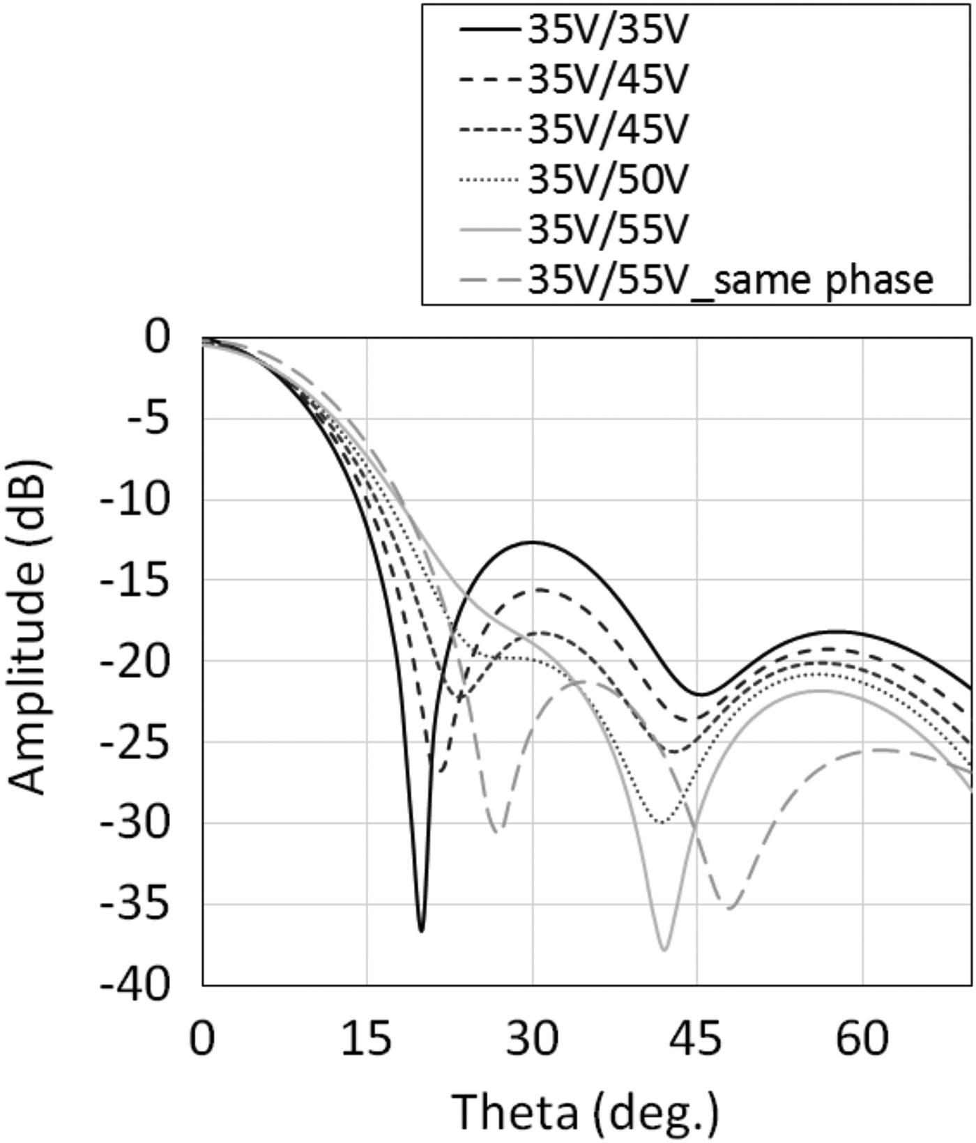
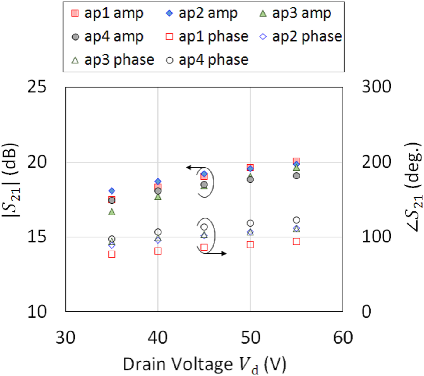
The antenna radiation patterns were calculated based on the measured amplifier output power and phase; the results are illustrated in Fig. 8. In the calculation, the port phase and amplitude of the edge of the array antenna are fixed to the values associated with a 35 V drain voltage for the amplifier based on the measured correlation shown in Fig. 9. On the other hand, the center antennas are tuned between teh amplitude and phase associated with the 35 and 55 V drain voltage. According to Fig. 8, the second sidelobe level of 6.6 dB is reduced by tuning the port amplitude and phase conditions. The main beam amplitude is hardly reduced. The first null point and sidelobe vanish when the 55 V conditions are applied to the center antennas because of the phase difference of the amplifiers for each drain voltage condition. According to Fig. 8, removing the phase difference of the amplifiers causes the null point and sidelobe to unfold. Therefore, it is concluded that the removal of the null point and sidelobe vanish is caused by the phase difference of the amplifiers.
Calculated antenna radiation patterns based on measured four-way amplifier output characteristics for each drain voltage condition.

Measured GaN amplifier S-parameters associated with different drain voltages.
IV. CHARACTERIZATION OF LOW-SIDELOBE ACTIVE ANTENNA
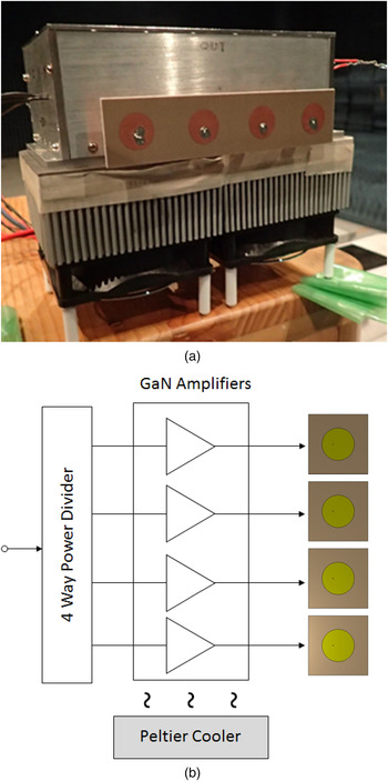
The fabricated four-way amplifier and antenna are combined, as shown in Fig. 10(a). The active-antenna component consists of the GaN amplifier, the antennas, and the power divider as shown in Fig. 10(b). The GaN amplifier is placed on a Peltier cooler (VICS LVPU-70), which serves to precisely control the surface temperature; the cooler can absorb up to 70 W, which is sufficient to eliminate the thermal effects on the GaN amplifier.
Fabricated 1 × 4 GaN active array antenna: (a) image and (b) configuration of GaN active-array antenna.

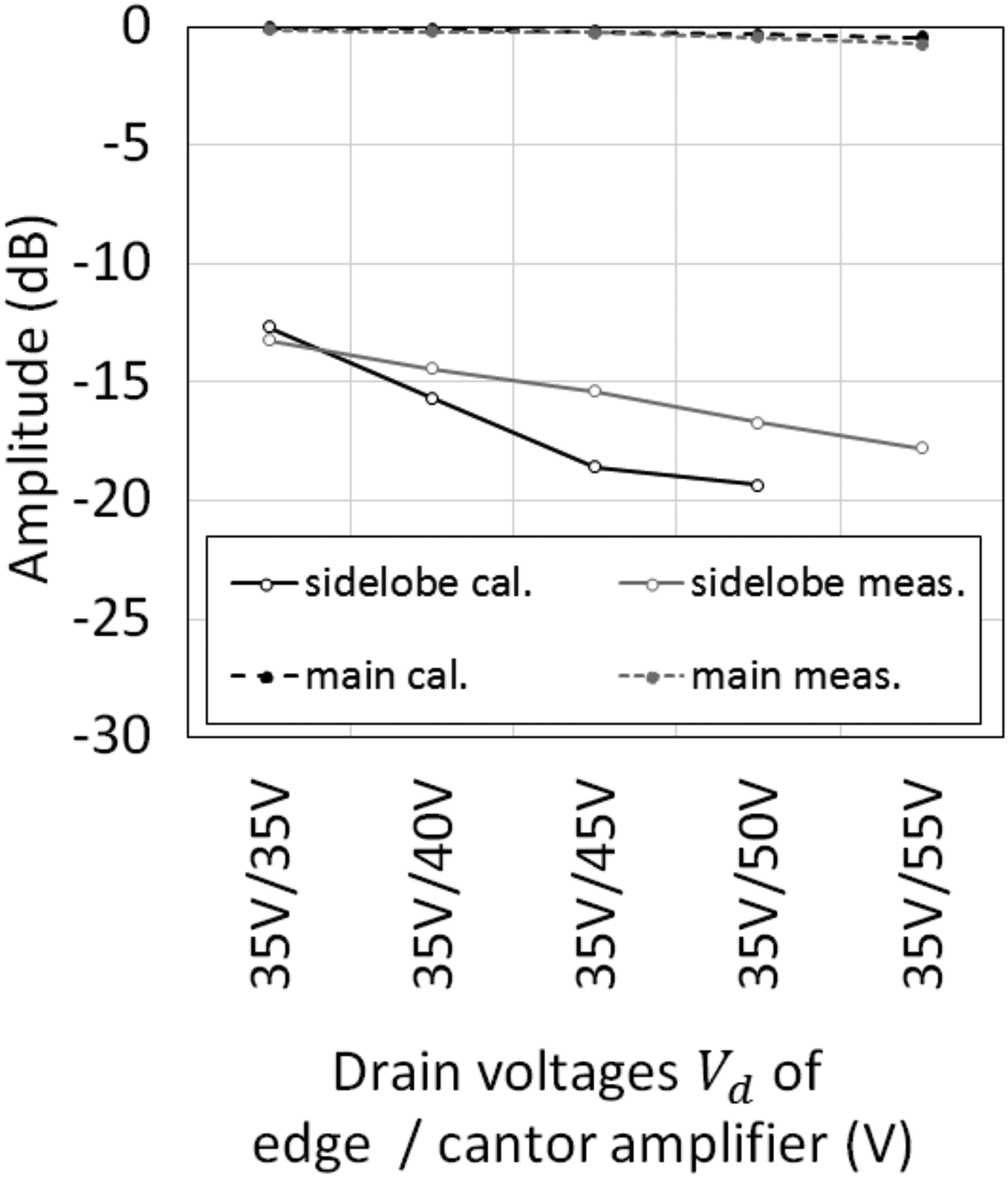
The measured main beam and sidelobe levels for various drain voltage conditions are illustrated in Fig. 11. In this measurement, the drain voltage of the center amplifiers is tuned between 35 and 55 V and the edge amplifiers are fixed to 35 V. According to Fig. 11, the measured main beam levels agree with the calculated results and sidelobe levels decrease as the drain voltage of the center amplifiers increase. In addition, by tuning the center-amplifier drain voltage from 35 to 55 V, the sidelobe level of 4.52 dB is reduced. In this experiment, the ability to reduce the sidelobe level of more than 50% by tuning the amplifier drain voltage is demonstrated.
Measured and calculated main beam and sidelobe amplitude for each drain voltage condition.

Furthermore, the equivalent isotropically radiated power (EIRP) for the front direction of the antenna is measured, which is important to characterize the performance of the active antenna. The EIRP is defined by the following equation,
 $$EIRP = P_{in} \times G_{ant},$$
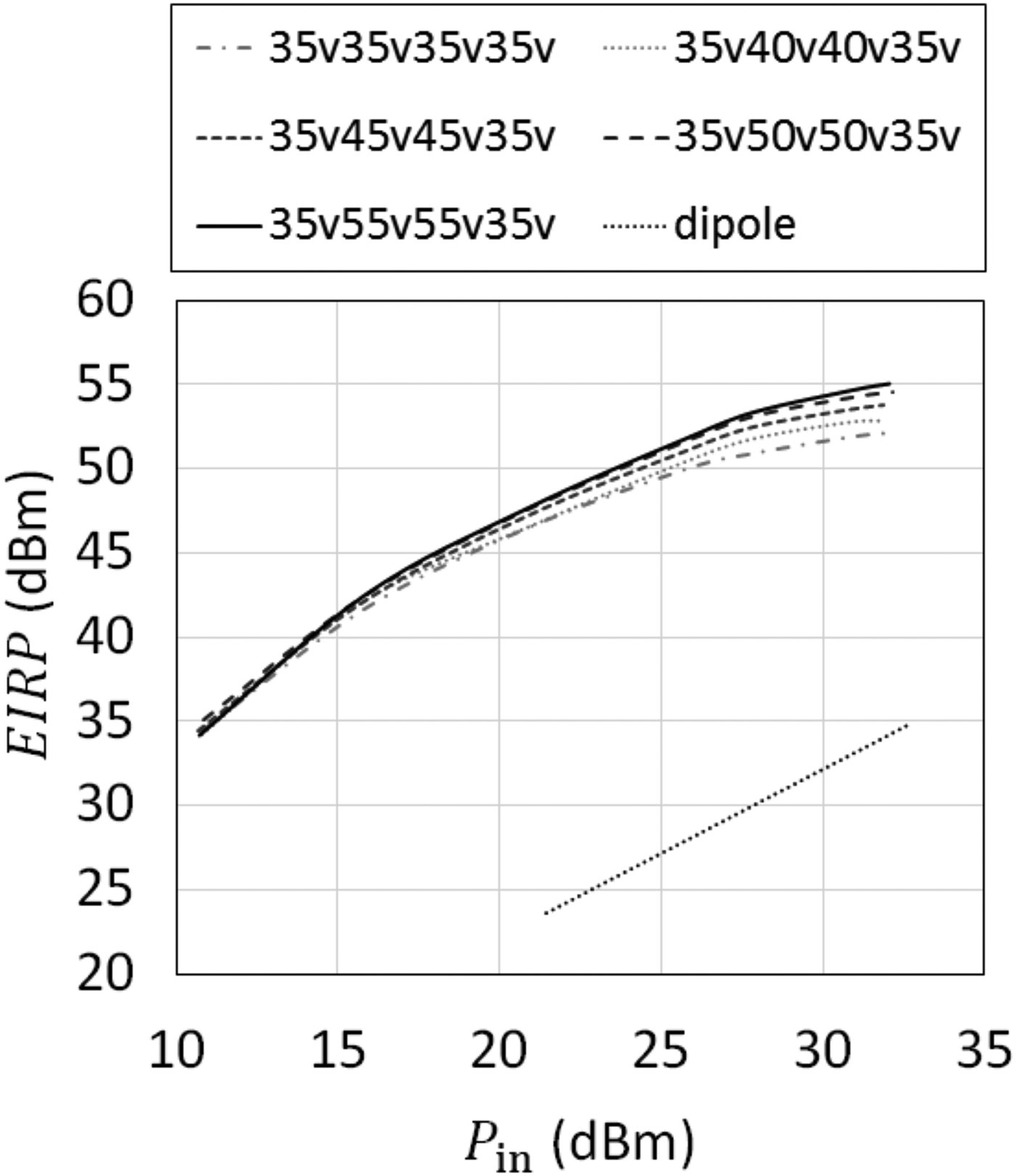
where P in is the input power to the antenna under test and G ant is the isotropic gain of antenna. In this study, G ant is measured by the gain-transfer method with a gain-standard dipole antenna. The measured EIRP of the GaN active antenna and dipole antenna are shown in Fig. 12. The measured maximum EIRP is 55.6 dBm at the 35/55 V drain voltage condition; this falls to 52.1 dBm in the 35/35 V condition because the total output power from the GaN amplifiers is reduced.
Measured front-direction EIRP of GaN active array antenna.

V. CONCLUSION
This study proposes a sidelobe reduction method based on a GaN active array antenna. In this method, the sidelobe level is tuned by adjusting the operating DC drain voltage of the amplifiers, which enables the situational switching of the radiation pattern. In this study, a single-stage GaN amplifier is designed and fabricated. The measured maximum output power is 39.3 dBm and the PAE is 59.6% at a 55 V DC drain voltage; when the drain voltage is decreased to 35 V, the output power decreases to 36.5 dBm. The amplifier output difference is proactively leveraged to realize sidelobe reduction. To do this, a four-way GaN amplifier is fabricated. The characteristics of the amplifiers are measured by a network analyzer and further used to calculate the antenna radiation pattern. The four-way GaN active-array antenna was tested, with the amplifier DC drain voltage varying from 35 to 55 V. According to the results, the 4.5 dB sidelobe level is reduced by tuning the operating center-amplifier drain voltage from 35 to 55 V, while the edge amplifiers are fixed to the 35 V condition. By this approach, it is possible to reduce the sidelobe level of more than 50% by tuning the amplifier drain voltage. Finally, the maximum EIRP for the front direction is measured as 55.6 dBm when the 35 V conditions are set for the edge amplifiers and the 55 V conditions are provided for the center amplifiers; this value is reduced to 52.1 dBm upon decreasing the center amplifier DC drain voltage condition to 35 V.
In this study, tunable sidelobe reduction based on the GaN active-antenna technique has been demonstrated effectively. We expect that the proposed technique will contribute to the broad realization and implementation of MPT systems. Sidelobes can cause electromagnetic interference, affect the human body, and cause a myriad of problems. Thus, this technique is useful for the situational sidelobe reduction necessary for a variety of future long-range MPT system for EVs, mobile phones, and sensor networks.
Acknowledgements
The authors would like to thank K. Sone, T. Orihara, M. Nishihara, S. Maruyama, N. Miyazawa, T. Yamamoto, T. Imamura, N. Kuwata, and T. Fujitani from Sumitomo Electric, for providing the high-power GaN-HEMT SG0601C. The authors would also like to thank T. Mitani and members of Shinohara laboratory, Kyoto University, for helpful discussions.
 Naoki Hasegawa was born in Aichi, Japan, on June 18, 1988. He received his B.E. degree in Electrical and Electronic Engineering from Ritsumeikan University, Siga, Japan, and his M.E. degree in Electrical Engineering from Kyoto University, Kyoto, Japan, in 2011 and 2013, respectively. He was a research associate in The Japan Aerospace Exploration Agency (JAXA) from 2013 to 2015. He is a student member of the Institute of Electronics, Information and Communication Engineers (IEICE) and the Institute of Electrical and Electronic Engineers (IEEE). His research activities include RF GaN power amplifier and antenna design for wireless power transfer and up-link satellite communications.
 Naoki Shinohara received the B.E. degree in Electronic Engineering, the M.E. and Ph.D. (Eng.) degrees in Electrical Engineering from Kyoto University, Japan, in 1991, 1993, and 1996, respectively. He was a research associate in Kyoto University from 1996. From 2010, he has been a professor in Kyoto University. He has been engaged in research on Solar Power Station/Satellite and Microwave Power Transmission system. He is IEEE MTT-S Technical Committee 26 (Wireless Power Transfer and Conversion) vice chair, IEEE MTT-S Kansai Chapter TPC member, IEEE Wireless Power Transfer Conference advisory committee member, International Journal of Wireless Power Transfer (Cambridge Press) executive editor, technical committee on IEICE Wireless Power Transfer, communications society member, Japan Society of Electromagnetic Wave Energy Applications vice president, Space Solar Power Systems Society board member, Wireless Power Transfer Consortium for Practical Applications (WiPoT) chair, and Wireless Power Management Consortium (WPMc) chair.