Introduction
In an ideal world, one would be able to cycle a phase-change memory device indefinitely, alternating between SET pulses for the crystalline phase (low resistance) and RESET pulses for the amorphous phase (high resistance), with the switching conditions and the resulting resistance states remaining completely stable. In practice, however, device characteristics change during cycling, at first slowly and then more rapidly, leading eventually to one of two failure modes: stuck-SET, in which the device stays in a low resistance state and refuses to RESET, or stuck-RESET, in which the device stays in a high-resistance state and refuses to SET.Reference Pirovano, Redaelli, Pellizzer, Ottogalli, Tosi, Ielmini, Lacaita and Bez1,Reference Yoon, Choi, Lee, Lee, Park and Yu2
At the early stages of phase-change memory research, it was suggested that the cycling endurance could be as high as 1012.Reference Lai3 However, various implementation efforts have resulted in agreement that the empirical endurance limit of typical phase-change memory cells is the range of 106–109, which is much better than NAND flash memory, but less than the desired limit of 1012 or even 1015 needed for working memory applications, where frequent and constant memory access is required. The improvement of cycling endurance is the main issue to be addressed for phase-change memory productsReference Cappelletti4 in order to expand and dominate the persistent memory market, which has the potential to grow to more than USD$1 billion/year in the next several years.Reference Webb5
It has been speculated that unlimited phase-change memory cycling endurance would not be possible because of the high temperatures (melting temperature typically at ∼900 K) that phase-change memory cells experience during the write operation. To raise the temperature above the melting temperature through Joule heating, the current density needs to be quite high, typically ∼10 MA/cm2, at which levels electromigration can occur in metal interconnects.Reference Wong, Raoux, Kim, Liang, Reifenberg, Rajendran, Asheghi and Goodson6 Also, the frequent volume changes due to the rise in temperature and changes in phases, which is roughly 7% between crystalline and amorphous Ge2Sb2Te5, for example,Reference Chen, Schrott, Lee, Raoux, Shih, Breitwisch, Baumann, Lai, Shaw, Flaitz, Cheek, Joseph, Chen, Rajendran, Lung and Lam7 could cause complex stress distributions in the phase-change memory cell. Successful R&D of various phase-change materials (PCMs) such as Ge2Sb2Te5 and GeTe has been able to address various important issues in phase-change memory because lots of key characteristics of phase-change memories (e.g., writing speed, retention, and programming power) are directly governed by corresponding materials properties (e.g., crystallization speed, crystallization temperature, and thermal conductivity, respectively). However, it has not been possible to identify a single or even a couple of materials properties that directly govern the cycling endurance.
In the following, we discuss and introduce various findings and models regarding the cycling endurance, such as failure mechanisms, key experimental results, and strategies, in order to improve phase-change memory endurance.
Driving forces
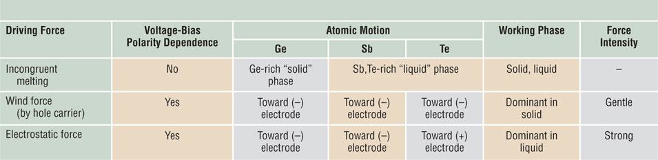
All phase-change memory cycling endurance failures can be linked to atomic migration. For example, the stuck-SET failure has been linked to atomic separation and compositional changes that result in a steady decrease in SET resistanceReference Sarkar and Gleixner8 and dynamic resistance,Reference Rajendran, Lee, Breitwisch, Burr, Shih, Cheek, Schrott, Chen, Lamorey, Joseph, Zhu, Dasaka, Flaitz, Baumann, Lung and Lam9 as well as RESET resistance changes.Reference Sarkar and Gleixner8–Reference Khwa, Wu, Su, Li, BrightSky, Wang, Hsu, Du, Kim, Chien, Cheng, Cheek, Lai, Zhu, Lee, Chang, Lung and Lam12 The stuck-RESET failures are linked to void formation.Reference Bae, Hwang, Park, Jeon, Choi, Ahn, Kim, Ahn, Jeong, Nam, Jeong, Cho, Jang and Park13 The main driving forces responsible for the atomic migration are summarized in Table I.
Driving forces behind atomic migration during phase-change memory operation.

It is known that the atoms within a heated phase-change memory are subject to a “hole-wind,” the momentum transfer from charge carriers to atoms, which has a strong effect in regions where the material is molten or undercooled liquid,Reference Nam, Kim, Kwon, Lee, Wi, Lee, Lee, Khang and Kim14–Reference Yang, Park, Kim and Joo16 but which can also have a lesser but eventual effect on the solid-crystalline material.Reference Park, Yang, Cho, Lee and Joo17,Reference Park, Cho, Jeong, Na and Joo18 The “hole-wind” force is a relatively gentle force, barely inducing momentum transfer to atoms. Instead, the wind force is effective for the motions of defect structures such as grain boundaries and dislocations during the phase-change memory cell programming.Reference Nam, Chung, Lo, Qi, Li, Lu, Johnson, Jung, Nukala and Agarwal19 On the other hand, the electrostatic force is more effective for inducing atomic motion. In contrast to the “hole-wind,” which pushes all elements in the same direction, the differing electronegativities of constituent atoms can cause each to move in different directions.Reference Nam, Kim, Kwon, Lee, Wi, Lee, Lee, Khang and Kim14,Reference Yang, Park, Kim and Joo16 In particular, based on their respective electronegativities, Sb atoms are likely to behave as cations while Te atoms behave as anions in the liquid phase. Thus, the electrostatic force present in the cell, typically more than 107 V/m, is regarded as the main force for inducing atomic separation.
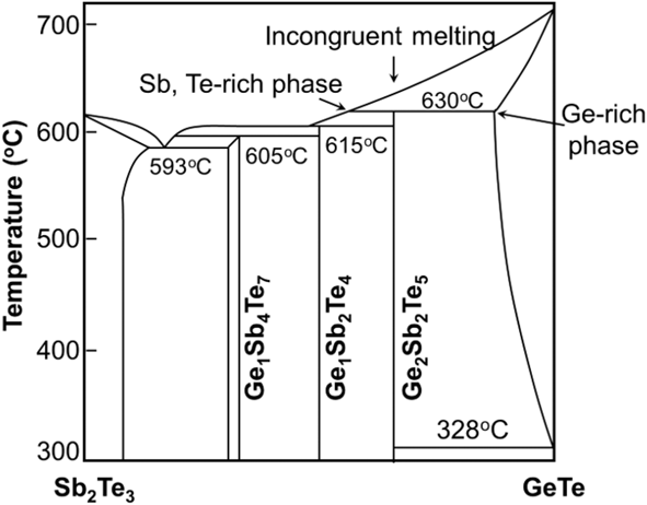
Atomic migration and void formation in phase-change memory have also been observed in experiments with temperature gradients, but with no electrical current or fields applied.Reference Do, Lee, Ko, Sohn and Cho20–Reference Yeoh, Ma, Cullen, Bain and Skowronski22 Concepts such as “incongruent melting” or “crystallization-induced segregation”Reference Debunne, Virwani, Padilla, Burr, Kellock, Deline, Shelby and Jackson21 have been proposed to account for these atomic migrations. The phase diagram of a PCM provides thermodynamic indications about its phase-separating behavior. For example, the pseudobinary phase diagram across the tie line between GeTe and Sb2Te3 (Figure 1) suggests that two phases can separate from Ge2Sb2Te5 upon heating/cooling through the two-phase region, during the repeated melt-quenching processes: One is a Ge-rich “solid” phase, and the other is a Sb- and Te-rich “liquid” phase. In terms of the actual kinetics involved, the process of crystallization is known to depend critically on stoichiometry.Reference Yamada, Ohno, Nishiuchi, Akahira and Takao23–Reference Raoux, Cheng, Caldwell and Wong25 Debunne and co-workers used this idea to introduce the concept of “crystallization-induced segregation”—when a stoichiometry that can rapidly crystallize establishes within an otherwise molten region of a PCM, this crystallization then excludes the elements not needed for that favorable stoichiometry. These elements remain in the molten phase and, over time, end up moving away from the expanding crystalline region, to the edges of the molten region. Similar mechanical forces are known to act upon PCMs as well, and to have considerable gradient effects.Reference Park, Jung, Ryu, Choi, Yu, Park, Han and Joo26,Reference Crespi, Lacaita, Boniardi, Varesi, Ghetti, Redaelli and D’Arrigo27
The pseudobinary phase diagram across the tie line between GeTe and Sb2Te3.

Device cycling endurance behaviors
Interactions among the various driving forces behind atomic migration result in several forms of cycling endurance behavior in phase-change memory cells. Early observations of intentionally damaged line-shaped structures revealed evidence of atomic motion from the original deposited stoichiometry,Reference Nam, Kim, Kwon, Lee, Wi, Lee, Lee, Khang and Kim14–Reference Yang, Park, Kim and Joo16 while failure analysis of cycled devices showed both atomic migration and void formation.Reference Lee, Cheek, Chen, Zhu, Bruley, Baumann, Shih, Lai, Breitwisch, Schrott, Raoux, Joseph, Cheng, Wu, Lung and Lam11,Reference Bae, Hwang, Park, Jeon, Choi, Ahn, Kim, Ahn, Jeong, Nam, Jeong, Cho, Jang and Park13 In addition, it has been observed that the voltage polarity has a strong effect on device endurance for any cell exhibiting physical device asymmetry. Applying a negative voltage to the top electrode of a device with a smaller bottom electrode has been shown to degrade endurance,Reference Lee, Cheek, Chen, Zhu, Bruley, Baumann, Shih, Lai, Breitwisch, Schrott, Raoux, Joseph, Cheng, Wu, Lung and Lam11 while a single pulse with a long tail (ramp-down) in this “bad” polarity direction can destroy a device immediately.Reference Padilla, Burr, Virwani, Debunne, Rettner, Topuria, Rice, Jackson, Dupouy, Kellock, Shelby, Gopalakrishnan, Shenoy and Kurdi28,Reference Padilla, Burr, Rettner, Topuria, Rice, Jackson, Virwani, Kellock, Dupouy, Debunne, Shelby, Gopalakrishnan, Shenoy and Kurdi29 However, judicious application of occasional pulses in the “bad” polarity direction,Reference Lee, Jeong, Lee, Kim and Cheong10 or reversal of polarity when using a symmetric device,Reference Goux, Tio Castro, Hurkx, Lisoni, Delhougne, Gravesteijn, Attenborough and Wouters30 have been shown to markedly extend endurance by counterbalancing the atomic migration.
In addition, it has been observed that using long pulses with excessive energy leads to lower enduranceReference Lai3,Reference Goux, Tio Castro, Hurkx, Lisoni, Delhougne, Gravesteijn, Attenborough and Wouters30 due to the acceleration of atomic migration, and that such “over”-RESET of devices can surprisingly lead to less resistance contrast,Reference Calderoni, Ferro, Varesi, Fantini, Rizzi and Ielmini31 yet cycling with overly weak RESET pulses also leads to lower enduranceReference Du, Wu, Hsu, Lee, Wang, Cheng, Lai, Lai, Lung, Kim, Breitwisch, Zhu, Mittal, Cheek, Raoux, Joseph, Schrott, Li and Lam32 due to earlier occurrence of stuck-SET failure.
We thus have a reasonable understanding of the behavior of the hot PCM within a device, as described by the full electrothermal and atomic-motion modeling performed by Novielli et al.Reference Novielli, Ghetti, Varesi, Mauri and Sacco33 These researchers were able to match experimental results with model predictions for atomic segregation in various types of phase-change memory cells.Reference Padilla, Burr, Rettner, Topuria, Rice, Jackson, Virwani, Kellock, Dupouy, Debunne, Shelby, Gopalakrishnan, Shenoy and Kurdi29,Reference Goux, Tio Castro, Hurkx, Lisoni, Delhougne, Gravesteijn, Attenborough and Wouters30,Reference Servalli34 The largest effect of the bias polarity is whether the hole-wind pushes the atomic elements toward or away from the hot region at the bottom contact. This explains why inverting the polarity can have such a pronounced effect. After that, electronegativity and elemental segregation effects will push elements either toward or away from the bottom electrode, leading either to distributions that exhibit reasonable endurance (“good” polarity) or distributions that can show poor endurance and even cause rapid device failure (“bad” polarity).
In general, Ge is most easily moved, but all elements in the typical GeSbTe alloys tend to move to some extent. At the same time, the Thomson effect, which describes the heating or cooling of a current-carrying conductor induced by a temperature gradient, is present in phase-change memory devices,Reference Castro, Goux, Hurkx, Attenborough, Delhougne, Lisoni, Jedema, Wolters, Gravesteijn, Verheijen, Kaiser, Weemaes and Wouters35 to an extent that is both observable in devices and has an impact on device characteristics.Reference Faraclas, Bakan, Adnane, Dirisaglik, Williams, Gokirmak and Silva36 This effect can then shift which region of the device gets the hottest under various voltage polarities.
Toward unlimited cycling endurance
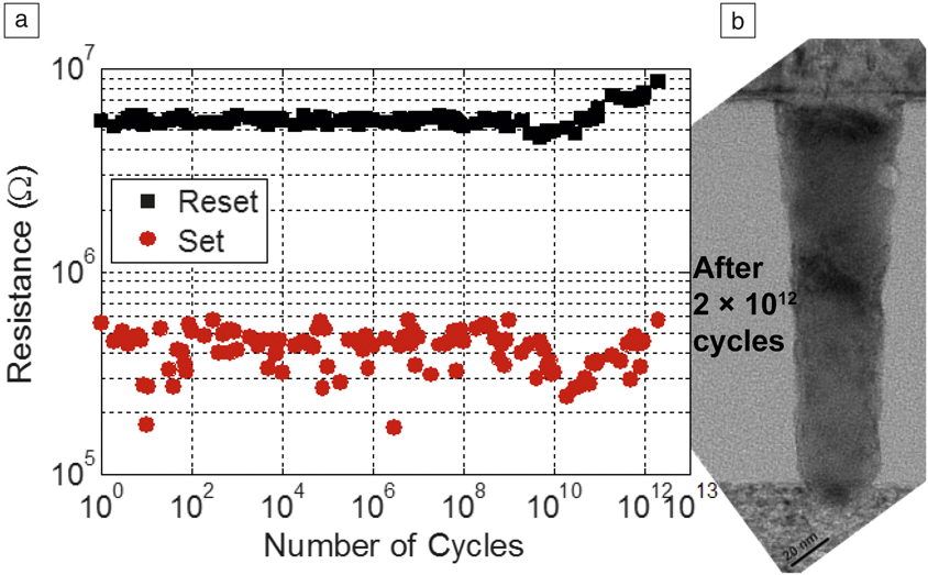
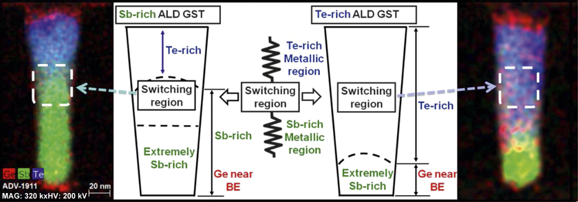
Based on the understanding of phase-change memory cycling endurance described in the previous sections, various ideas have been suggested to delay or even completely avoid cycling endurance failures in phase-change memory devices. To avoid stuck-SET failures, one could use a monatomic PCM such as Sb.Reference Salinga, Kersting, Ronneberger, Jonnalagadda, Vu, Le Gallo, Giannopoulos, Cojocaru-Mirédin, Mazzarello and Sebastian37,Reference Zhang and Ma38 On the other hand, if elemental segregation is unavoidable, one can devise a phase-change memory cell geometry such that elemental segregation would not result in stuck-SET failure, such as the confined phase-change memory cell shown in Figure 2.Reference Kim, BrightSky, Masuda, Sosa, Kim, Bruce, Carta, Fraczak, Cheng, Ray, Zhu, Lung, Suu and Lam39 This cell is much more symmetric than typical mushroom-shaped (i.e., a large PCM island contacted by a small cylindrical heater) phase-change memory cells. This ensures that even after repeated cycling, the composition that can be efficiently RESET-programmed stays in the center of the pore (a small hole with cylindrical shape) (Figure 3), as confirmed by in situ transmission electron microscope (TEM) analysis.Reference Kim, Kim, Bruce, Carta, Fraczak, Ray, Lam, BrightSky, Zhu, Masuda, Suu, Xie, Kim and Cha40 The extremely segregated regions near the top and bottom electrodes simply serve as extended electrodes, thus avoiding stuck-SET failure.
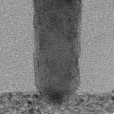
(a) Confined phase-change memory with a metallic liner exhibits a high endurance of 2 × 10¹² cycles. This cell remains functional after 2 × 10¹² cycles. (b) Cross-sectional transmission electron microscope image of the cell after 2 × 10¹² cycles shows dense, void-free phase-change memory inside the pore.

(Center) Schematics illustrating the switching region and elemental segregation during cycling in a (left) Sb-rich confined phase-change material cell with a metallic liner and (right) in a Te-rich confined phase-change memory cell with a metallic liner. (Left, right) Elemental maps of the two cells created with energy-dispersive x-ray analysis. For both types of cell, the phase-change memory pore is extremely Sb-rich near the bottom electrode (BE) and extremely Te-rich near the top electrode. Each segregated region is metallic and serves as an extended electrode. Note: ALD GST, atomic layer deposition GexSbyTez.

To avoid stuck-RESET failures, various techniques to prevent void formation have been proposed. It has been shown that doping the PCM could result in less thermal stress, potentially due to the smaller thermal expansion and volume change between phases.Reference Chen, Schrott, Lee, Raoux, Shih, Breitwisch, Baumann, Lai, Shaw, Flaitz, Cheek, Joseph, Chen, Rajendran, Lung and Lam7,Reference Cheng, BrightSky, Raoux, Chen, Du, Wu, Lin, Hsu, Zhu, Kim, Lin, Ray, Lung and Lam41 Another scheme is to minimize the amount of minuscule voids that could coalesce into a large void by densifying the as-deposited PCM with high-temperature anneals.Reference BrightSky, Sosa, Masuda, Kim, Kim, Ray, Bruce, Gonsalves, Zhu, Suu and Lam42 An additional technique reported to extend the cycling endurance is to heal the void after its creation. Kim et al.Reference Kim, Kim, Bruce, Carta, Fraczak, Ray, Lam, BrightSky, Zhu, Masuda, Suu, Xie, Kim and Cha40 showed for the first time that confined phase-change memory could have a self-recovery property by incorporating a metallic liner, which provides an additional conduction path even with neighboring large voids and initiates the recovery process. Experimental results using real-time in situ TEM have shown that the confined phase-change memory can recover by self-void elimination during regular programming operation.Reference Kim, Kim, Bruce, Carta, Fraczak, Ray, Lam, BrightSky, Zhu, Masuda, Suu, Xie, Kim and Cha40,Reference Xie, Kim, Kim, Kim, Gonsalves, BrightSky, Lam, Zhu and Cha43
To improve the phase-change memory cycling endurance, both stuck-SET and stuck-RESET should be avoided because either of them, whichever occurs earlier, will cause the phase-change memory to fail.Reference Kim, Du, Li, Breitwisch, Zhu, Mittal, Cheek, Hsu, Lee, Schrott, Raoux, Cheng, Lai, Wu, Wang, Joseph, Lai, Ray, Lung and Lam44 A novel confined phase-change memory cell with dense PCM formed by atomic layer deposition and a thin metallic linerReference Kim, BrightSky, Masuda, Sosa, Kim, Bruce, Carta, Fraczak, Cheng, Ray, Zhu, Lung, Suu and Lam39 can extend programming endurance to 2 × 10¹² cycles, as shown in Figure 2. This device successfully addresses both stuck-SET and stuck-RESET failures through several of the aforementioned techniques, such as symmetric cell geometry, densification of the as-deposited PCM, and self-void healing.
Conclusion and outlook
A recent demonstration of a phase-change memory device with very high cycling endurance of up to 2 × 10¹² cycles indicates that in-depth study of endurance failure mechanisms, based on principles of materials science, can lead to successful development of various engineering techniques to extend the cycling endurance to a level which has previously been considered difficult to achieve. It would be worthwhile to investigate whether these cycling endurance enhancement techniques can be applied to other novel PCM compositions, especially those with ultrafast writing speeds,Reference Rao, Ding, Zhou, Zheng, Xia, Lv, Song, Feng, Ronneberger, Mazzarello, Zhang and Ma45 which could enable the direct replacement of conventional dynamic and static random access memory with phase-change memory.

SangBum Kim is an assistant professor in the Department of Materials Science and Engineering at Seoul National University, Republic of Korea. He received his BS degree from Seoul National University, and his MS and PhD degrees from Stanford University, all in electrical engineering. From 2010 to 2018, he was with the IBM T.J. Watson Research Center, conducting research on phase-change memory devices for various memory applications such as storage-class memory, embedded memory, and brain-inspired neuromorphic computing. His current research interests include novel synaptic materials and devices designed from the ground up for neuromorphic computing, and novel memory devices. Kim can be reached by email at sangbum.kim@snu.ac.kr.

Geoffrey W. Burr is a distinguished research staff member at IBM Research–Almaden. He received his PhD degree in electrical engineering from the California Institute of Technology in 1996. His research includes holographic data storage, photon echoes, computational electromagnetics, nanophotonics, computational lithography, phase-change memory, storage-class memory, and novel access devices based on mixed-ionic-electronic conduction materials. His current research focuses on nonvolatile memory and cognitive computing. Burr can be reached by email at gwburr@us.ibm.com.

Wanki Kim is a research staff member at the IBM T.J. Watson Research Center. He received his BS degree from the Korea Advanced Institute of Science and Technology in 2005, Republic of Korea, and his MS degree in 2008 and his PhD degree in 2012 from Stanford University, all in electrical engineering. His current research focuses on phase-change memory and selectors for storage-class memory and phase-change memory-based synaptic devices for deep learning. Kim can be reached by email at wkim@us.ibm.com.

Sung-Wook Nam is an assistant professor in the School of Medicine at Kyungpook National University, Republic of Korea. He received his BS degree in 2003, and his PhD degree in 2009 in materials science and engineering from Seoul National University, Republic of Korea. He completed postdoctoral research and was a research fellow at the University of Pennsylvania, the IBM T.J. Watson Research Center, and the Institute for Basic Science, Republic of Korea. His research focuses on integrating nano-bio devices and in situ electron microscopy of electronic materials, including phase-change materials. Nam can be reached by email at nams@knu.ac.kr.