Introduction
The discovery of large photovoltages up to 15 V in multiferroic BiFeO3 films has attracted increased attention towards ferroelectrics photovoltaics [Reference Yang, Seidel, Byrnes, Shafer, Yang, Rossell, Yu, Chu, Scott, Ager, Martin and Ramesh1]. Different from traditional semiconductor solar cells, the photovoltaic effect in ferroelectrics relies on the polarization-induced internal electric field instead of p–n or Schottky junctions, which not only improves the separation and migration of light-generated electron-hole pairs but also breaks the limit of photo-induced voltages in traditional semiconductor solar cells (the E g of light absorbers, approximately 1 V) [Reference Zhang, Wu, Li, Huang, Yang, Huang, Liao and Lin2, Reference Choi, Lee, Choi, Kiryukhin and Cheong3]. However, most of the current ferroelectric oxides have wide band gaps (E g > 2.7 eV for BiFeO3 and E g > 3.5 eV for PZT) that are beyond the visible-light range and thus allow the use of only 8–20% of the solar spectrum [Reference Wang, Grinberg and Rappe4, Reference Choi, Chisholm, Singh, Choi and Jellison5], which may be one of the major obstacles that limit the photovoltaic application of ferroelectrics. Therefore, a strategy to reduce the band gap of ferroelectrics without losing the useful ferroelectricity will bring significant scientific and technological breakthroughs. To overcome these aforementioned drawbacks, Grinberg et al. mixed the perovskite ferroelectric oxide KNbO3 (KNO) with BaNi0.5Nb0.5O3−δ (BNNO) to introduce Ni2+ to the B-site and oxygen vacancies, which gave band gaps of 1.1–2.0 eV in the resulting [KNbO3]1−x[BaNi1/2Nb1/2O3−δ]x (KBNNO) materials, matching the solar spectrum [Reference Grinberg, West, Torres, Gou, Stein, Wu, Chen, Gallo, Akbashev, Davies, Spanier and Rappe6]. Based on this, Zhou et al. offered further insights into the room-temperature ferromagnetism (RTFM) of KBNNO ceramics [Reference Zhou, Deng, Yang and Chu7]. Previous studies have pointed out that the bulk phases of KBNNO have to be synthesized by the solid-state reaction under the harsh conditions of high temperature. These drawbacks of KBNNO materials inevitably limit their practical applications in photoelectric devices, especially in room-temperature environments. Compared with ceramics, films occupy an important position in the field of actual device preparations. Therefore, research on narrow-band gap ferroelectric films is imperative.
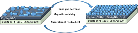
Here, we introduced Na element into the KBNNO system, taking the similar crystal structure and superior stability performance of the K0.5Na0.5NbO3(KNNO) film compared with KNO into consideration [Reference Pithan, Shiratori, Dornseiffer, Haege, Magrez and Waser8, Reference Saito, Takao, Tani, Nonoyama, Takatori, Homma, Nagaya and Nakamura9, Reference Li, Wang, Zhu, Cheng, Yao and Green10, Reference Bortolani, Campo, Fernandez, Clemens and Rubio11]. In this paper, KNBNNO films were firstly synthesized by a mild chemical solution deposition method. Using our method, the KNBNNO films can be fabricated directly on different substrates on a large scale, and the thickness of the films can be well controlled, which established a good basis for further research and application of large-scale film perovskite solar cells in the future. In addition, the microstructure, surface morphology, optical properties, ferromagnetism, and substrate effects of KNBNNO films were investigated in our work, and we found that BNNO content was a key factor in determining the properties of the final products. Moreover, the interesting magnetism-switch phenomenon was observed for KNBNNO films. It is noteworthy that absorption behavior in the visible light wave band for KNBNNO films has been realized, indicating that it is possible to use KNBNNO films for perovskite solar cell applications. These results are used to gain insights into the origin and understanding of structural transition, band-gap tuning, and magnetic variation mechanism in perovskite-type film materials. We hope that our work will inspire more experimental explorations of KNBNNO films as a candidate material for use in multiferroic and solar-energy applications.
Results and discussion
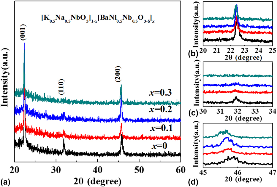
Taking the absence of the standard powder XRD pattern of KNNO into consideration and according to the similar diffraction peaks of the standard powder sample of K0.65Na0.35NbO3 (JCPDS card No. 77-0038), it can be seen that all the as-prepared samples show a pure perovskite phase structure [Reference Deng, Zhang, Huang, Xu, Jiang, Li, Hu and Chu12, Reference Lee, Kim, Ahn, Ullah, Lee and Kim13, Reference Ye, Liu, He, Cao, Kang, Chen, Yan and Mei14, Reference Tanaka, Kakimoto and Ohsato15], at least within the detection limits of the instrument (see Fig. 1). All recorded XRD patterns are indexed as single-phase pseudo-cubic (pc) perovskite structures [Reference Kopnin, Istomin, D’yachenko, Antipovl, Bordet, Capponi, Chaillout, Marezio, Brion and Souletie16, Reference Venkatesh, Sherman and Setter17]. The peak profiles at around 46° in the XRD patterns, which did not show an obvious splitting phenomenon, were used as evidence for confirming the structure of KNNO films [Reference Tanaka, Hayashi, Kakimoto, Ohsato and Iijima18, Reference Yi, Liu, Carpenter, Schiemer and Withers19, Reference Yu, Li, Sun, Zhou, Xu, Xie, Lai and Wang20]. Moreover, it can be obviously observed that the peak varies with the composition of the KNBNNO system, as shown in Figs. 1(c) and 1(d). With increasing BNNO content, (110) peaks start to get weakened and gradually disappear, and (200) peaks shift toward lower angle, which confirms the presence of lattice expansion [Reference Zhang, Zhang, Yin, Zhang, Chen, Wang and Wu21]. This behavior is due to the introduction of Ni2+ cations, with a larger ionic radius (0.69 Å) than Nb5+ (0.64 Å). The above analysis also indicates that the Ni2+ cation doped KNNO can produce an inner stress field, which breaks the balance of Nb–O orbital hybridization, inducing lattice distortion, which is in agreement with Zhou’s work [Reference Zhou, Deng, Yang and Chu7].
(a) XRD patterns of KNBNNO films synthesized at 700 °C on quartz substrates with different x values, (b) magnified patterns around 2θ = 22°, (c) magnified patterns around 2θ = 32°, and (d) magnified patterns around 2θ = 45°.
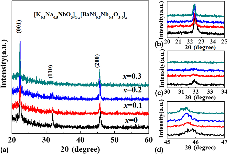
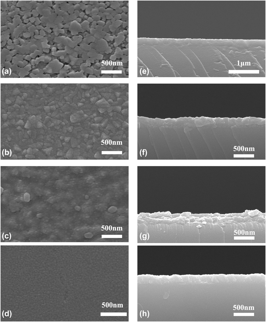
Figure 2(a)–2(d) show the typical SEM images of the as-prepared KNBNNO polycrystalline films synthesized at 700 °C on a quartz substrate with x = 0.0, 0.1, 0.2, and 0.3, respectively. Morphological differences have been clearly observed in KNBNNO polycrystalline films at different BNNO contents. Loosened, heterogeneous, and agglomerated irregular films are observed in KNBNNO polycrystalline films when x = 0, as seen in Fig. 2(a). However, the porosity and the grain size decrease with the increase of BNNO doping, as presented in Figs. 2(b)–2(d). Based on the particle growth inhibition in the KBNNO ceramics system [Reference Rani, Yadav and Prakash22, Reference Ramam and Lopez23], we explained this phenomenon as follows: Ba2+ at A-site generates K+ vacancies, which results in domain pinning accompanying the lower particle growth rate, eventually leading to a decrease in the particle size. The thicknesses of KNBNNO films can be calculated from the cross-sectional micrographs, which are about 200 nm, as seen in Figs. 2(e)–2(h).
SEM surface morphologies (a–d) and cross-sectional images (e–h) of KNBNNO films synthesized at 700 °C on quartz substrates.

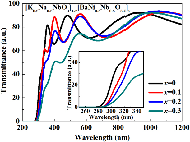
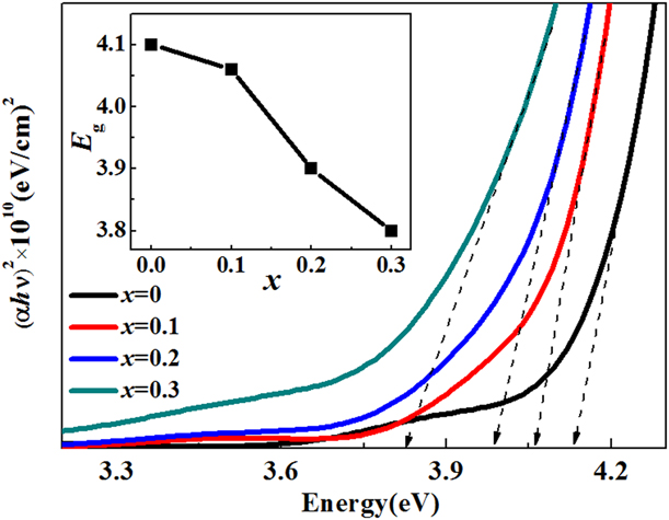
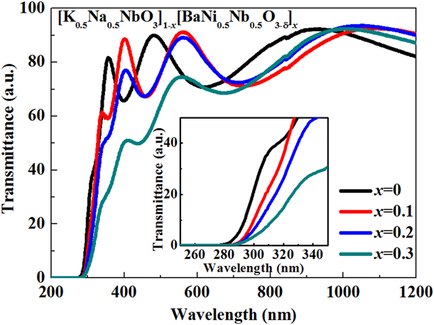
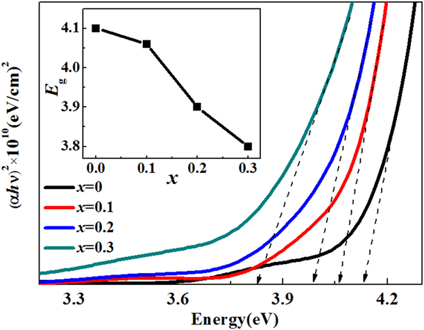
Figure 3 shows the transmittance spectra of the KNBNNO films synthesized at 700 °C on a quartz substrate measured using an ultraviolet–visible–near-infrared spectrophotometer. The optical transmittance properties are relevant to the electronic structure features and band gap. The transmittance for all the KNBNNO films decreases to zero at a wavelength of 280 nm, which approximately corresponds to the material band gap [Reference Deng, Zhang, Huang, Xu, Jiang, Li, Hu and Chu12]. It is apparent that the band gap absorption edges of the samples exhibit a sequential red shift with increasing the BNNO content, as shown in the inset of Fig. 3. The corresponding optical band gaps (E g) of the KNBNNO films can be estimated from the tangent lines in the Tauc plot of (αhν)2 versus hν for a direct-band gap material, where α is the absorbance and hν is the photon energy [Reference Tauc and Grigorovici24], as presented in Fig. 4. The slope of the linear part suggests the band gap of KNNO to be 4.10 eV, which agrees with that reported in prior studies [Reference Deng, Zhang, Huang, Xu, Jiang, Li, Hu and Chu12], and those of the other three KNBNNO (x = 0.1, 0.2, and 0.3) are 4.06 eV, 3.91 eV, and 3.79 eV, respectively. In the fundamental absorption edge regions, the absorption is due to the band-to-band transition from the top of the valence band (VB) to the bottom of the conduction band (CB) directly. For KNNO, the top of the VB arises mainly from the O 2p orbitals and the bottom of the CB is essentially set by the Nb 4d orbitals [Reference Su, Jiang, Gong and Zhai25]. Based on the prior studies [Reference Zhou, Deng, Yang and Chu7], the lower band gap of KNBNNO is due to the band-to-band transition from hybridized Ni 3d and O 2p to Nb 4d states. The filled Ni 3d gap states in KBNNO therefore play a crucial role in lowering the band gap. Different substrates may play a significant role in the formation of different crystal structures, which control the chemical and physical properties of the material. The obvious band gap decrease behavior was present for KNBNNO films grown on Pt(111)/Ti/SiO2/Si(100) substrates. The details will be discussed in a later section.
The transmittance spectra of the KNBNNO films synthesized at 700 °C on quartz substrates with different x values and the magnified transmittance spectra of the KNBNNO films (inset).
Plots of (αhν)2 versus hν for the transmittance spectral data.
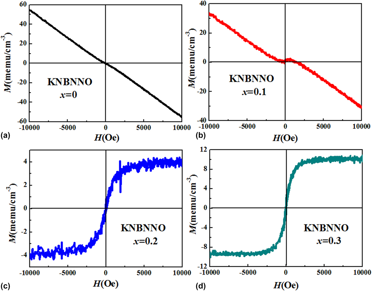
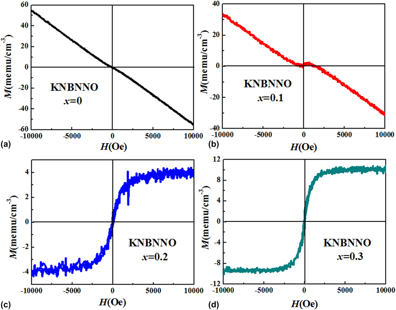
The magnetization versus magnetic field (M–H) curves of KNBNNO films synthesized at 700 °C on a quartz substrate measured with a maximum magnetic field of 10 kOe at room temperature are shown in Fig. 5. For the sample with x = 0, in which no magnetic element was doped, a weak anti-S-type M–H curve is obtained, demonstrating that the pure KNNO film is intrinsically diamagnetic. For the sample with x = 0.1, because of the introduction of Ni2+ ions, superexchange interactions between Ni2+ and Ni2+ emerged, which mainly dominates the magnetic behavior of the KNBNNO film. The superexchange interactions between Ni2+ and Ni2+ are antiferromagnetic in nature, which suppress the diamagnetism of the KNBNNO film, resulting in a rapid decrease in magnetic moment. But with a further increase of the Ni2+ ions, a typical S-type hysteresis for ferromagnetic materials is obtained, indicating the emergence of ferromagnetic long-range ordering in KNBNNO films with x = 0.2 and x = 0.3. The maximum saturation magnetization (M S), 10 emu/cm−3, has been also observed for x = 0.3. The ferromagnetic behavior in KNBNNO films can be explained as follows [Reference Jalbout, Chen and Whittenburg26, Reference Matsukura, Ohno, Shen and Sugawara27, Reference Coey, Venkatesan and Fitzgerald28, Reference Zhou, Deng, Yu, Yang and Chu29]: The origin of magnetism is due to the exchange interaction between local-spin polarized electrons and conduction electrons. This interaction leads to the spin polarization of conduction electrons. Subsequently, the spin polarization conductive electrons have an exchange interaction with spin-polarized electrons of other Ni ions. Thus, after the long-range exchange interaction, almost all Ni moments align in the same direction, inducing ferromagnetism in the KNBNNO material. For the x = 0.2 and x = 0.3 compositions, lattice defects such as oxygen vacancies (VO2−) are easily formed in the KNBNNO film, which leads to the generation of bound electrons to maintain charge neutrality with oxygen loss during processing. These localized electrons and Ni2+ ions may form bound magnetic polarons, which occupy a Bohr orbit and mediates the ferromagnetic ordering of Ni dopants within this orbital. The electron trapped in the VO2− occupies an orbital, which overlaps the d shells of both Ni2+ neighbors. A ferromagnetic exchange interaction between the magnetic Ni2+ ions and a spin-polarized electron trapped at oxygen vacancies (Ni2+–VO2−–Ni2+) leads to ferromagnetic ordering throughout the KNBNNO film with x = 0.2 and x = 0.3 compositions.
M–H hysteresis dada of the KNBNNO films on quartz substrates at room temperature: (a) x = 0, (b) x = 0.1, (c) x = 0.2, and (d) x = 0.3.
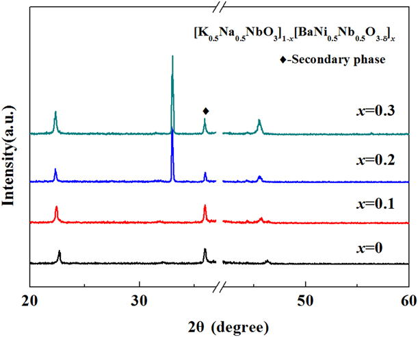
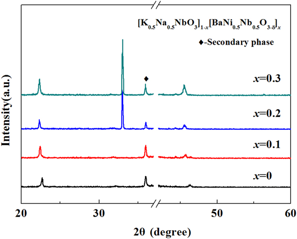
Different substrates may play a significant role in the formation of different crystal structures [Reference Zhai, Jia, Zhang, Lei, Wei, Gao, Chu, He, Yin and Zheng30, Reference Yan, Deng, Ding, He, Peng, Sun, Yang and Chu31]. The extreme sensitivity of many properties to structural distortions and crystal chemistry also provides various routes to control and engineer new functionalities in these systems. The KNBNNO films were deposited on Pt(111)/Ti/SiO2/Si(100) substrates, keeping other synthetic conditions constant. The XRD patterns, as seen in Fig. 6, indicate that the films exhibit a (110)-highly oriented pseudo-cubic perovskite crystal structure, and the KNbO3 secondary phase was observed. Compared with the XRD patterns of KNBNNO films with x = 0.3 at 700 °C on quartz substrates, the preferred orientation changes from the (001) plane to the (110) plane. This variation can be attributed to the surface interfacial effect [Reference Zhai, Deng, Zhou, Yang and Chu32].
XRD patterns of KNBNNO films with different x values at 700 °C on Pt(111)/Ti/SiO2/Si(100) substrates.
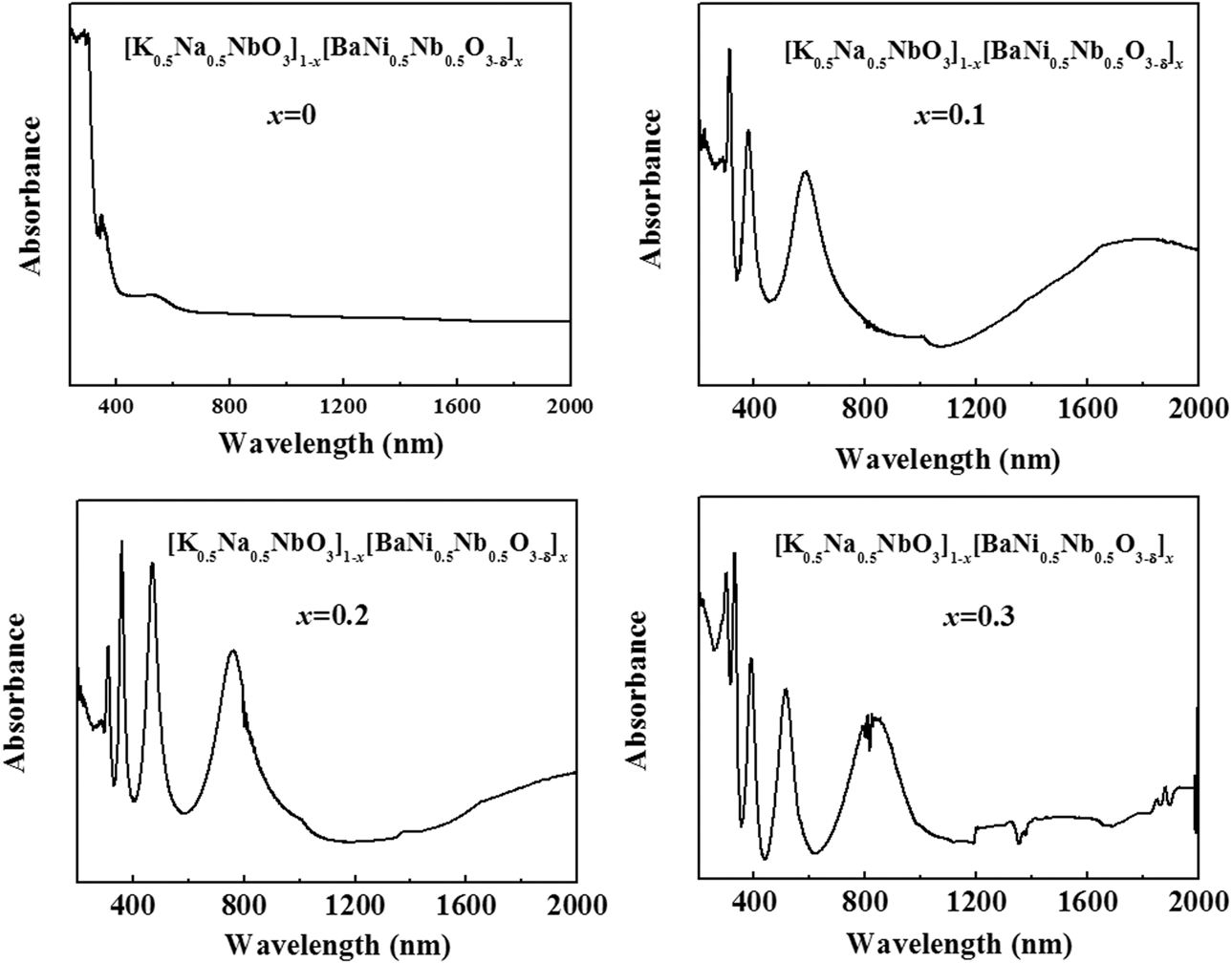
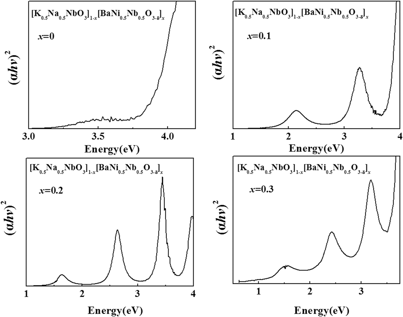
The ultraviolet–visible–near-infrared absorption spectra of the KNBNNO films with different x values at 700 °C on Pt(111)/Ti/SiO2/Si(100) substrates are shown in Fig. 7. For the sample with x = 0, the absorption was mainly concentrated in the ultraviolet region. But because of the introduction of Ni2+ ions, the absorption range gradually transitioned to the visible and near-infrared region. Moreover, with a further increase of the Ni2+ ions, the absorption of the samples exhibits a mild red-shift phenomenon. The corresponding optical band gaps (E g) of KNBNNO films can be estimated from the tangent lines in the plot of Kubelka–Munk function (αhν)2 versus hν for a direct-band gap material, where α is the absorbance and hν is the photon energy, as seen in Fig. 8 [Reference He, Sun, Chen, Chen, Yang and Chu33]. For the sample with x = 0.3, the band gap edges were near 410 nm, 560 nm, and 960 nm, which indicated that there are three different electron leap behaviors for KNBNNO films on Pt(111)/Ti/SiO2/Si(100) substrates. As presented in Fig. 8, the slope of the linear part suggests the band gaps to be, in the order, 1.28, 2.20, and 3.0 eV. We could not explain this multiple electron leap phenomenon exactly, and we just speculated the reasons for this phenomenon within the scope of our abilities. The 3.0 eV band gap may be indexed to electron leaps from the top of the VB arising mainly from the O 2p orbitals and the bottom of the CB is essentially set by the Nb 4d orbitals in the KNbO3, which agreed with the XRD result. The 2.20 eV band gap may be indexed to electron leaps from the top of the VB arising mainly from the O 2p orbitals and the bottom of the CB is essentially set by the impurity energy level, which is lower in energy than the Nb 4d orbital. The 1.28 eV band gap may originate from the intraband transition of the Ni 3d orbital, namely, the electron leaps from the  ${d_{{z^2}}}$ to
 ${d_{{x^2} - {y^2}}}$ orbital. For the KNBNNO film, the Ni and O vacancies replace Nb and the Ni 3d orbitals fall in the KNNO band gap. In this case, the VB is localized around Ni, which is mainly
 ${d_{{z^2}}}$, the highest filled d-orbital for d 8 Ni2+ in a square-planar configuration. And the CB is localized around Ni 3d states, resembling
 ${d_{{x^2} - {y^2}}}$. The energy of the Ni 3d orbital is lower than that of the Nb 3d orbital, which is similar with the increasing conduction band tail states [Reference Zhou, Deng, Yu, Yang and Chu29, Reference Su, Wang, Meng, Han and Wang34].
UV–vis–NIR absorption spectra of the KNBNNO films with different x values at 700 °C on Pt(111)/Ti/SiO2/Si(100) substrates.

Plots of (αhν)2 versus hν for the absorption spectra.

Conclusion
In summary, KNBNNO films were deposited on quartz and Pt(111)/Ti/SiO2/Si(100) substrates by a chemical solution deposition method. The microstructure, surface morphologies, and optical and magnetic properties of KNBNNO films on quartz substrates were investigated. The effects of BNNO composition on the phase formation of KNBNNO films as well as the physical properties were further discussed. According to the XRD results, KNBNNO films on quartz substrates undergo lattice distortion with increasing the BNNO content from 0 to 0.3. The observed lattice distortion mainly stems from the Ni2+ doping-induced local lattice strain. Additionally, the particle size, band gap and magnetism of KNBNNO films can also be controlled by the BNNO doping content. It is noted that with increasing x from 0 to 0.3, the magnetism of the samples undergoes an interesting transition from diamagnetism to ferromagnetism, originating from the competition between ferromagnetic exchange interactions in Ni2+–VO2−–Ni2+ and superexchange interactions in Ni2+–Ni2+. The electron leap behaviors of KNBNNO films on Pt(111)/Ti/SiO2/Si(100) substrates also indicated that the KNBNNO film is a promising material for use in photovoltaic devices. These results are helpful in deeper understanding of the relation between the crystal structure and the physical properties of perovskite oxides. We hope that our work will inspire more experimental explorations of KNBNNO films as a candidate material for use in multiferroic and solar-energy applications.
Experimental details
The ferroelectric KNBNNO films were deposited on quartz and Pt(111)/Ti/SiO2/Si(110) substrates by chemical solution deposition employing a spin-coating process. In order to monitor the effect of BNNO composition on the microstructure and optical properties, the KNBNNO films were prepared in the x range of 0 ≤ x ≤ 0.3 at 0.1 intervals. Analytically pure sodium acetate (CH3COONa, 99.0%), potassium acetate (CH3COOK, 99.0%), barium acetate [(CH3COO)2Ba, 99.0%], nickelous acetate (C4H6NiO4, 99.0%), and niobium ethoxide [(CH3CH2O)5Nb, 99.0%] were mixed in stoichiometric composition (10 mol% excess K and Na were added to compensate for the loss of alkaline metals during thermal annealing) as starting materials for the preparation of KNBNNO precursor solutions. Acetic acid glacial (CH3COOH, 99.5%) and 2-methoxyethanol (CH3OCH2CH2OH, 99.0%) were used as solvents. Acetyl-acetone (CH3COCH2COCH3, 99.0%) was used as a chelating agent. Note that all of the chemical reagents and solvents used in the experiment were purchased from commercial sources and of analytical grade without any further purification. All the KNBNNO precursor solutions were stirred using a magnetic stirrer in a constant temperature bath. The concentration of the final solution was adjusted to 0.2 mol/L, which was filtered by using a 0.22 μm pore size filter. Prior to deposition, the substrates were cleaned in pure acetone and ethanol in an ultrasonic bath to remove oily substances and other impurities from the surfaces, followed by rinsing several times with deionized water, then the substrates were dried in a pure nitrogen stream. To obtain KNBNNO films, the precursor solutions were spin-coated onto the processed quartz and Pt(111)/Ti/SiO2/Si(100) substrates. The films were deposited by employing a spin-coating process at a speed of 3000 rpm for 20 s. Each layer of the films was dried at 200 °C for 200 s to evaporate the solvent and then pyrolyzed at 380 °C for 200 s to remove residual organic compounds, followed by annealing at 650–700 °C for 300 s to crystallize the films by a rapid thermal annealing procedure. The spin-coating and annealing treatment procedures were repeated ten times to obtain the desired thickness.
The crystalline structure of the KNBNNO films was investigated by X-ray diffraction (XRD; Bruker D8 Advance, Bruker AXS GmbH, Karlsruhe, Germany) with a Cu Kα radiation source. In the XRD measurement, a continuous scanning mode (θ–2θ) was selected with a step size of 0.2° and a collection time of 0.1 s. The surface morphology and cross section were characterized by scanning electron microscopy (SEM; Philips XL30FEG, Philips, Holanda). The magnetic properties of the samples were tested by a physical property measurement system (PPMS-9; Quantum Design, Inc. (QD) is the manufacturing arm of Quantum Design International (QDI), San Diego, California). The optical transmittance experiments were carried out by an ultraviolet–visible–near-infrared spectrophotometer (cary500, Varian, Palo Alto, California). All measurements of the samples were performed at room temperature.
Acknowledgments
This work was supported by the National Natural Science Foundation of China (61474045) and the State Key Basic Research Program of China (2013CB922300).