Introduction
Graphene is a single sheet of hexagonally bonded sp 2 carbon atoms with two carbon atoms per unit cell. This arrangement gives rise to extraordinary physical properties, including ultrahigh intrinsic carrier (electron and hole) mobility, gate-tunable ambipolar carrier density, high current-density capacity, long-distance ballistic and spin transport, exceptionally low electronic noise, high thermal conductivity, and high elastic modulus—all of which were recently discussed and illustrated in an earlier MRS Bulletin articleReference First, de Heer, Seyller, Berger, Stroscio and Moon1 (also see the introductory article and the article by Ruan et al. in this issue). In addition, graphene devices can be fabricated using ostensibly the same techniques as currently employed by the silicon industry. These extraordinary attributes have attracted widespread attention for advanced device concepts including ultrasensitive molecular sensors;Reference Schedin, Geim, Morozov, Hill, Blake, Katsnelson and Novoselov2 ultrafast, ultrawideband optical saturable absorbers,Reference Xing, Guo, Zhang, Sum and Huan3 transparent conductors,Reference Kim, Zhao, Jang, Lee, Kim, Ahn, Kim, Choi and Hong4 and other photonic and optoelectronic applications;Reference Bonaccorso, Sun, Hasan and Ferrari5 Klein-tunneling heterojunction devices;Reference Young and Kim6 nanoelectromechanical systems;Reference van der Zande, Barton, Alden, Ruiz-Vargas, Whitney, Pham, Park, Parpia, Craighead and McEuen7 electrical signal frequency multipliers;Reference Wang, Nezich, Kong and Palacios8 electronic spin-transport devices;Reference Tombros, Jozsa, Popinciuc, Jonkman and van Wees9 and high-frequency (on the order of terahertz) field-effect transistors (FETs).Reference Champlain10
Yet, despite this immense technological potential, realizing the promise of pervasive device applications depends on the ability to controllably make large-area, uniformly thick, defect-free graphene layers on substrates compatible with current commercial processing technology. At this time, there are only two prospective approaches for making large-area graphene layers: (1) silicon sublimation from SiC substrates (described in this article) and (2) catalyzed growth on copper and other metal substrates (described in the article by Bartelt and McCarty in this issue).
Formation of epitaxial graphene (EG) on SiC probably first occurred in the 1890s, when Edward Acheson developed a process for making SiC abrasives.Reference Acheson11 His experiments on heated SiC indicated sublimation of silicon, leaving behind graphitic carbon12 on the surface; this process presumably, and without his knowledge at the time, started with the formation of graphene.
The underpinnings of the mechanism of graphene formation advanced in 1975 when Van Bommel et al.Reference Van Bommel, Crombeen and Van Tooren13 reported differences in the rate of carbon formation between the two polar faces of SiC designated (0001) (the “Si face”) and (000 $\overline {\rm{1}} $) (the “C face”). Whereas the Si face undergoes a surface reconstruction, found to be (6√3 × 6√3)R30°, the C face lacks any complex reconstruction. Forbeaux et al.Reference Forbeaux, Themlin and Debever14 reported that the evolution of the (0001) surface as a function of annealing temperature indicated a graphitic structure. In 2002, Charrier et al.Reference Charrier, Coati, Argunova, Thibaudau, Garreau, Pinchaux, Forbeaux, Debever, Sauvage-Simkin and Themlin15 controlled the rate of Si sublimation from a highly doped n + 6H-SiC(0001) substrate by varying the temperature to form a few layers of graphene that had a lattice parameter comparable to that of graphite. In 2004, Berger et al.Reference Berger, Song, Li, Li, Ogbazghi, Feng, Dai, Marchenkov, Conrad, First and de Heer16 were the first to demonstrate the extraordinary electron-transport properties of EG formed by physical desorption of silicon from SiC under ultrahigh-vacuum (UHV) conditions.
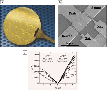
The first wafer-scale formation of EG, using a UHV process, was performed in 2007 on a 76-mm (diameter) wafer.Reference Gaskill, Nyakiti and Murali17 This was followed in 2008 by wafer-scale growth using an intermediate-vacuum process on a 50-mm waferReference Gaskill, Nyakiti and Murali17 and soon after by an argon-mediated process, also on a 50-mm wafer.Reference Gaskill, Nyakiti and Murali17 Wafer-scale graphene formation enabling the realization of a graphene-based FET was one of several crucial steps successfully achieved within the US Defense Advanced Research Projects Agency (DARPA) Carbon Electronics for RF Applications (CERA) program; other essential steps were layer-thickness control and uniformity over the entire wafer (deviation of no more than one layer). In addition, the CERA program resulted in wafer-scale processing of dozens of 50- and 76-mm wafers that permitted accelerated development of graphene FETs, as reported in a recent review.Reference Garces, Wheeler and Gaskill18Figure 1 shows examples of an EG wafer processed into FETs, an individual FET device, and device electrical characteristics.Reference Moon, Curtis, Hu, Wong, McGuire, Campbell, Jernigan, Tedesco, VanMil, Myers-Ward, Eddy and Gaskill20 More recently, wafer-scale EG played a significant role in the noteworthy FET cutoff frequency performance of 200 GHz for gate lengths of 210 nm,Reference Lin, Farmer, Jenkins, Wu, Tedesco, Myers-Ward, Eddy, Gaskill, Dimitrakopoulos and Avouris21 the first prototype integrated circuits,Reference Lin, Valdes-Garcia, Han, Farmer, Meric, Sun, Wu, Dimitrakopoulos, Grill, Avouris and Jenkins22 and the first demonstration of a top-gated nanoribbon FET with a 10-nm width.Reference Hwang, Tahy, Nyakiti, Wheeler, Myers-Ward, Eddy, Gaskill, Xing, Seabaugh and Jena23
(a) Processed graphene field-effect transistors (FETs) on 50-mm-diameter 6H-SiC wafer. The wafer was processed by HRL Laboratories within the Defense Advanced Research Projects Agency (DARPA) Carbon Electronics for RF Applications (CERA) program. (b) Scanning electron microscopy image of an epitaxial graphene (EG) FET patterned on an EG epiwafer with a gate length of 0.25 μm (courtesy of J.S. Moon, HRL Laboratories, Malibu, CA). (c) Current–voltage curves, drain–source current (I DS) versus drain–source voltage (V DS) for various gate–source voltages (V GS), showing both p- and n-channel FET functionality characteristic of zero-bandgap graphene. Reproduced with permission from Reference Reference Moon and Gaskill19. ©2011, Institute of Electrical and Electronics Engineers.

This article describes the approach and scientific issues associated with the formation of graphene on SiC substrates. In particular, the impacts of the substrate, surface preparation, and synthesis conditions on the uniformity and reproducibility of epitaxial graphene are described. Moreover, the crucial aspects of reactor design required to achieve large-area uniformity for wafer-scale EG formation are discussed. Finally, important directions for future research in EG are highlighted.
Key elements of epitaxial graphene synthesis
The key elements for EG synthesis include the quality of the substrate, specifically its orientation and surface preparation; the sublimation conditions; and the control and uniformity of the process conditions over the sample. In particular, defects originating from the substrate have been shown to impact graphene formation.Reference Hite, Twigg, Tedesco, Friedman, Myers-Ward, Eddy and Gaskill24
Substrate quality
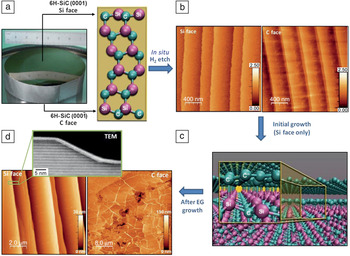
SiC exhibits about 200 crystalline lattice forms, or polytypes,Reference Masri25 each consisting of an equal number of carbon and silicon atoms that are predominantly covalently bonded, but distinguished by geometrically different C–Si bilayer stacking sequences. The large-format SiC wafers required for commercial electronics are primarily produced in the hexagonal polytypes denoted 4H and 6H. Semi-insulating (SI) 4H- and 6H-SiC wafers are typically 100 mm in diameter, although 76-mm wafers are still offered. Substrates of the same diameter are also available in highly doped (n-type conductivity) form, and an example boule of n + 6H-SiC is shown in Figure 2a; however, SI substrates are normally used for graphene synthesis to permit electrical isolation of FETs.
(a) The highly reflective face of a 76-mm-diameter crystalline boule of 6H-SiC (image courtesy of WBG Materials, Pine Brook, NJ [a subsidiary of II-VI Incorporated]) and schematic of two polar SiC faces. (b) Morphologies of hydrogen-etched Si- and C-face surfaces (adapted from Reference Reference VanMil, Myers-Ward, Tedesco, Eddy, Jernigan, Culbertson, Campbell, McCrate, Kitt and Gaskill26). (c) Schematic of the interface layer on Si-face graphene, where C′ and C″ represent carbon atoms bonded to the SiC substrate and not bonded to the substrate, respectively (image courtesy of Marco Buongiorno Nardelli, University of North Texas, Denton, TX, and Thushari Jayasekera, Southern Illinois University, Carbondale, IL). (d) Atomic force microscopy (AFM) images of as-grown Si-face and C-face epitaxial graphene (EG) and transmission electron microscopy (TEM) image of as-grown Si-face EG (AFM images adapted from Reference Reference VanMil, Myers-Ward, Tedesco, Eddy, Jernigan, Culbertson, Campbell, McCrate, Kitt and Gaskill26; TEM image courtesy Josh Robinson, Pennsylvania State University, University Park, PA).

For the production of large-area epitaxial graphene on SiC to be feasible and to provide reproducible properties, the underlying substrate must be of high, uniform crystal quality. This requirement can be met with state-of-the-art SiC wafer technology.Reference Eddy and Gaskill27 The overall quality of current SiC wafers is excellent: The presence of micropipes—open core dislocations with a large Burgers vector (i.e., >2[0001])—is a thing of the past, as their densities can be less than 1 cm–2; polytype control is almost fully achieved; crystallinity, defined by x-ray diffraction full width at half-maximum (FWHM), is uniform over the wafer and exhibits values of <30′′; and uniform resistivity above 1010 Ω cm, important for radio-frequency (RF) applications, is easily obtained. In addition, 150-mm-diameter wafer technology has been announced and should be available in the near future.28 For the purposes of this article, we focus on the formation of graphene on SI 4H- and 6H-SiC, on which most research has been conducted to date.
EG synthesis on the two polar faces of SiC, the Si and C faces mentioned previously (Figure 2a), results in very different growth mechanisms,Reference Hite, Twigg, Tedesco, Friedman, Myers-Ward, Eddy and Gaskill24, Reference Ohta, Bartelt, Nie, Thürmer and Kellogg29 morphologies,Reference VanMil, Myers-Ward, Tedesco, Eddy, Jernigan, Culbertson, Campbell, McCrate, Kitt and Gaskill26 growth rates, and electrical properties.Reference First, de Heer, Seyller, Berger, Stroscio and Moon1 In the following discussion, we briefly review the growth details for the polar faces, including recent insights that impact wafer-scale growth.
Regardless of polarity, surface preparation of the SiC substrate prior to graphene synthesis is an essential element for achieving high-quality and uniform epitaxial graphene. In situ hydrogen etching is conducted before graphene formation to remove any polishing damage and to produce a uniform morphology with C–Si bilayer steps. Optimized etch parameters create terraces defined by nearly parallel steps having heights corresponding to two to six C–Si bilayers (Figure 2b).Reference VanMil, Myers-Ward, Tedesco, Eddy, Jernigan, Culbertson, Campbell, McCrate, Kitt and Gaskill26 (For example, the 4H Si face yields two bilayers or 0.5-nm step heights, and the 6H C face yields six bilayers or 1.5-nm step heights.)
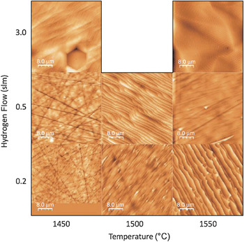
Increasing the etch temperature can degrade the SiC morphology, leading to jagged step edges or extended defects etched into the substrate that are subsequently reproduced in the graphene layer on Si-face substrates; see examples in Figure 3.Reference Ostler, Speck, Gick and Seyller30 Additionally, studies of Si-face EG have shown that protrusions and irregular initial step morphology can disrupt step-flow growth, resulting in variations in graphene thickness across the terraces formed during synthesis.Reference Ohta, Bartelt, Nie, Thürmer and Kellogg29
Atomic force microscopy images of hydrogen-etched SiC surfaces for various hydrogen flow rates (in standard liters per minute, slm) and temperatures. For this experimental matrix, the best results were achieved with a hydrogen flow of 0.5 slm at 1500°C. Reproduced with permission from Reference Reference Ostler, Speck, Gick and Seyller30. ©2010. Wiley.

On the Si face, growth is initiated by the formation of a carbon-rich interface layer (IFL) between the SiC substrate and the graphene layer. The IFL, variously called “layer 0” or the “buffer layer,” is depicted in Figure 2c and has a (6√3 × 6√3)R30° structure. Ohta et al.Reference Ohta, Bartelt, Nie, Thürmer and Kellogg29 showed that subsequent graphene synthesis proceeds by a step-flow and carbon-diffusion mechanism. A simple description of this process consists of silicon sublimating at a step edge, resulting in step retraction across the surface and thus producing a step-bunched (greater than a C–Si bilayer step) morphology (Figure 2d), typically having a height of 5–10 nm. In this way, the step edges act as a source of excess carbon on the surface that then diffuses to form a continuous graphene film over the adjacent terrace and the step (Figure 2d inset); an additional graphene layer is often found at the step edge.
Process conditions, such as increased temperature or time, can be modified to increase the layer count on the terraces and steps.Reference Bolen, Harrison, Biedermann and Capano31 The ensuing graphene morphology is highly dependent on the initial SiC morphology, which, in turn, impacts the diffusion of carbon across the surface. This can lead to nonuniform layer thicknesses. Under optimized hydrogen-etching and growth conditions, monolayer graphene is attained on the terracesReference Robinson, Wetherington, Tedesco, Campbell, Weng, Stitt, Fanton, Frantz, Snyder, VanMil, Jernigan, Myers-Ward, Eddy and Gaskill32 over the entire substrate in about 10–30 min.
The electron-transport properties of monolayer graphene grown in this way are influenced by the IFL. Because not all of the bulk silicon atoms at the interface are bonded to the IFL, the resulting silicon dangling bonds induce electron doping of the overlying graphene layer.Reference Emtsev, Speck, Seyller, Ley and Riley33–Reference Varchon, Feng, Hass, Li, Nguyen, Naud, Mallet, Veuillen, Berger, Conrad and Magaud36 Typically, this charge transfer is between ∼5 × 10¹² and 1 × 1013 cm–2,Reference Tedesco, VanMil, Myers-Ward, McCrate, Kitt, Campbell, Jernigan, Culbertson, Eddy and Gaskill37 and the experimental 300 K mobility is approximately (1–2) × 103 cm2 V–1 s–1.
In comparison, growth on the C face is markedly different than that on the Si face.Reference Tedesco, Jernigan, Culbertson, Hite, Yang, Daniels, Myers-Ward, Eddy, Robinson, Trumbull, Wetherington, Campbell and Gaskill38 Using a narrow range of temperatures and pressures, Hite et al.Reference Hite, Twigg, Tedesco, Friedman, Myers-Ward, Eddy and Gaskill24 showed that the step-flow growth seen on the Si face is replaced by local nucleation and expansion on the C face. Defects, specifically screw dislocations in the underlying SiC substrate that thread through to the surface, increase the local silicon sublimation rate, resulting in graphene nucleation sites across the sample. These nucleation sites continue to act as sources of carbon, which might diffuse away from the site. Moreover, because the sublimation process results in the removal of about three bilayers of the SiC latticeReference Hass, de Heer and Conrad39 per monolayer of EG formed, the graphene lies at the flat bottom of a basin containing the threading screw dislocation (TSD). Growth proceeds by expansion of these graphene-covered basins (GCBs) as the edges act as silicon-sublimation/carbon-diffusion sources, eventually encountering other GCBs, which might be oriented differently and/or have different sizes because the nucleation process is stochastic. Hence, the fully coalesced film contains misoriented grains and exhibits nonuniform thickness. In addition, for sufficiently thick films, thermal expansion differences with the substrate result in wrinkles during coolingReference Prakash, Bolen, Colby, Stach, Capano and Reifenberger40 (Figure 2d). Silicon sublimation and carbon diffusion from the TSDs are very efficient, and quite thick graphene films (10–100 layers) can be formed in less than 1 h. This growth mechanism explains the general features of rotationally faulted, Bernal (ABA) and rhombohedral (ABC) stacking sequences as reported by others.Reference Borysiuk, Soltys and Piechota41, Reference Hass, Feng, Li, Li, Zong, de Heer, First, Conrad, Jeffrey and Berger42 The defect-assisted growth mechanism on the C face results in a much faster and less controllable growth process than that on the Si face for a broad range of process conditions.
The differences between EG obtained on the C and Si faces extend beyond the growth mechanism to very different EG–SiC interface structures and transport properties. For instance, unlike EG on the Si face, EG on the C face has no interface layer between the bulk SiC and graphene layers. Thus, no significant charge is induced in the C-face graphene, and the charge density varies with layer depth;Reference Lin, Dimitrakopoulos, Farmer, Han, Wu, Zhu, Gaskill, Tedesco, Myers-Ward, Eddy, Grill and Avouris43 the graphene layer(s) closest to the substrate are slightly n-type due to dangling bonds of the carbon rest atom in the SiC(000 $\overline {\rm{1}} $)-(2 × 2)C surface reconstruction (Figure 4),Reference Sidorov, Gaskill, Nardelli, Tedesco, Myers-Ward, Eddy, Jayasekera, Kim, Jayasingha, Sherehiy, Stallard and Sumanasekera44 whereas intermediate layers are nearly intrinsic due to charge screening,Reference Jernigan, VanMil, Tedesco, Tischler, Glaser, Davidson, Campbell and Gaskill45–Reference Orlita, Faugeras, Plochocka, Neugebauer, Martinez, Maude, Barra, Sprinkle, Berger, de Heer and Potemski47 and the layer exposed to the ambient is doped p-type due to an electrochemically mediated charge transfer from –OH groups from the ambient.Reference Sidorov, Gaskill, Nardelli, Tedesco, Myers-Ward, Eddy, Jayasekera, Kim, Jayasingha, Sherehiy, Stallard and Sumanasekera44 As an aggregate, the graphene layers typically act as p-type (∼[0.2–1] × 1013 cm–2) with a relatively high 300 K mobility of (1–3) × 104 cm2 V–1 s–1.Reference VanMil, Myers-Ward, Tedesco, Eddy, Jernigan, Culbertson, Campbell, McCrate, Kitt and Gaskill26, Reference Tedesco, VanMil, Myers-Ward, McCrate, Kitt, Campbell, Jernigan, Culbertson, Eddy and Gaskill37, Reference Berger, Song, Li, Wu, Brown, Naud, Mayou, Li, Hass, Marchenkov, Conrad, First and de Heer48 At this time, EG on the C face is less desirable for high-frequency device applications because the charge density is generally high and varies with depth, which makes device gating difficult. For this reason, the rest of this article focuses on EG grown on the Si face.
Ball-and-stick diagram showing the SiC(000 $\overline {\rm{1}} $)-(2 × 2)C surface reconstruction at the interface with graphene, where Si′ is the silicon adatom and C′ is the carbon rest atom (adapted from Reference Reference Sidorov, Gaskill, Nardelli, Tedesco, Myers-Ward, Eddy, Jayasekera, Kim, Jayasingha, Sherehiy, Stallard and Sumanasekera44).

Sublimation conditions
Sublimation conditions such as pressure, ambient composition, temperature, and growth duration are all key aspects in engineering epitaxial graphene properties. Specifically, changes in pressure dramatically change the morphology and electrical properties of EG.Reference VanMil, Myers-Ward, Tedesco, Eddy, Jernigan, Culbertson, Campbell, McCrate, Kitt and Gaskill26, Reference Bolen, Harrison, Biedermann and Capano31 When synthesized under UHV conditions, EG has an irreproducible, rough morphology consisting of irregular steps and terraces; as described in the preceding subsection, this leads to nonuniform graphene thickness. In addition, a high concentration of pitting is a common surface feature that gives UHV-grown EG a “Swiss cheese” appearance.Reference de Heer49 Increasing the pressure during EG synthesis to an intermediate vacuum level (∼10–6–10–4mbar) considerably reduces surface roughness and enhances thickness uniformity, when compared to UHV-grown layers.Reference Bolen, Harrison, Biedermann and Capano31
Introduction of argon into the growth environmentReference Emtsev, Bostwick, Horn, Jobst, Kellogg, Ley, McChesney, Ohta, Reshanov, Rohrl, Rotenberg, Schmid, Waldmann, Weber and Seyller50 changes the growth dynamics and effectively decreases the growth rate by decreasing the silicon sublimation rate as compared to the rates obtained by the intermediate-vacuum and UHV synthesis methods.Reference Langmuir51, Reference Fonda52 The reduction of the growth rate consequently enables surface reconstruction to be fully completed before graphene formation on the surface. This produces an EG morphology similar to that achieved by the intermediate-vacuum process (Figure 2d) with the added benefit that it significantly improves both the magnitude and the uniformity of carrier mobility.Reference Emtsev, Bostwick, Horn, Jobst, Kellogg, Ley, McChesney, Ohta, Reshanov, Rohrl, Rotenberg, Schmid, Waldmann, Weber and Seyller50, Reference Tedesco, VanMil, Myers-Ward, Culbertson, Jernigan, Campbell, McCrate, Kitt, Eddy and Gaskill53
Control and uniformity of the process conditions
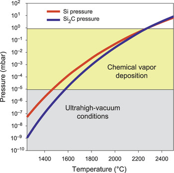
Growth temperature and durationReference Bolen, Harrison, Biedermann and Capano31 both have significant impacts on the graphene thickness, although a greater influence is seen with the former. As the pressure–temperature phase diagram shows (Figure 5),Reference Gaskill, Jernigan, Campbell, Tedesco, Culbertson, VanMil, Myers-Ward, Eddy, Moon, Curtis, Hu, Wong, McGuire, Robinson, Fanton, Stitt, Stitt, Snyder, Wang and Frantz54 at a fixed pressure, an increase in temperature results in increased silicon sublimation, thereby enabling the subsequent carbon release to form thicker EG; this means that uniformity of temperature is essential to uniformity of graphene thickness. As is well known,Reference Sarma, Adam, Hwang and Rossi56 the electrical properties of graphene depend on the number of layers. Hence, variations in processes can result in variations in graphene properties. Such process–property relationships require additional systematic investigations to permit further advances in improving EG properties.
Pressure–temperature phase diagram for volatile silicon and Si2C over SiC. For a given temperature, the necessary vacuum conditions can be determined to remove the sublimated silicon from the sample, thus enabling graphene growth. Model calculated with the parameters used by Lilov.Reference Lilov55 Reproduced with permission from Reference Reference Gaskill, Jernigan, Campbell, Tedesco, Culbertson, VanMil, Myers-Ward, Eddy, Moon, Curtis, Hu, Wong, McGuire, Robinson, Fanton, Stitt, Stitt, Snyder, Wang and Frantz54. ©2009, Electrochemical Society.

Toward uniform, reproducible large-area EG
As discussed in the preceding section, to realize graphene-based device technologies on large-area SiC substrates, it is essential to have superior-quality large-area substrates and a process designed to control uniform graphene formation over the substrate diameter. The former prerequisite can be met with existing commercial products, albeit with the added requirement that the surface be precisely oriented to the crystal lattice, as further explained in the next paragraph. This is followed by a description of the approaches to control and uniformity of process conditions over wafers practiced in our laboratory, as an example.
A crucial requirement for SiC wafers suitable for homogeneous graphene formation is the uniformity of the wafer orientation. It should be noted that it is not possible to achieve a precise wafer surface orientation because of vagaries in wafer processing technology, namely, orienting and sawing boules, as well as polishing the cut slices to produce wafers. A variation in orientation from the basal plane is quantitatively described as “off-cut.” Small (large) off-cuts typically correspond to large (small) terrace widths. It has been shown that the growth rate and step-bunch height of graphene grown on the Si face are functions of terrace width and, hence, are directly traceable to the off-cut.Reference Robinson, Trumbull, LaBella, Cavalero, Hollander, Zhu, Wetherington, Fanton and Snyder57 Typical off-cuts for nominally “on-axis” wafers from various vendors sampled by our laboratory ranged from 0° to 0.8° toward [11 $\overline {\rm{2}} $0] or [1
 $\overline {\rm{1}} $00]. It is noted that off-cuts approaching 0° produce wide terraces that can be highly desirable for device fabrication. This is because wide terraces enable device placement to avoid step bunches, which have been shown to give rise to conductance inhomogeneities.Reference Yakes, Gunlycke, Tedesco, Campbell, Myers-Ward, Eddy, Gaskill, Sheehan and Laracuente58 In particular, it was recently shown that placement of the entire active region of an FET on a terrace rather than overlapping a step bunch yielded a record-high cutoff frequency of ∼210 GHz.Reference Lin, Farmer, Jenkins, Wu, Tedesco, Myers-Ward, Eddy, Gaskill, Dimitrakopoulos and Avouris21 Hence, a uniform, low off-cut is a desirable SiC wafer characteristic for graphene formation.
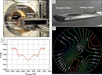
In addition to the substrate requirements, the design of the reactor in which the graphene is grown is critical to achieving reproducible large-area, uniform graphene formation. In our laboratory, epitaxial graphene is grown in an Aixtron VP50859 horizontal hot-wall chemical vapor deposition (CVD) reactor that includes all of the necessary attributes preferred for large-scale uniform growth. As shown in Figure 6a, samples are placed in a susceptor made of dense high-purity graphite consisting of ceiling, bottom, satellite (wherein the samples are positioned), and sidewalls, with graphite foam insulation surrounding the dense material, insulating the process tube from the high temperatures at the sample (∼1600°C). Gases, specifically ultrahigh-purity hydrogen and argon, are introduced from the upstream portion of the reactor through a quartz liner and are fed into the susceptor through a graphite adaptor in such a way as to establish laminar flow across the substrate surface. The gases are exhausted through a process pump, where the pressure is controlled by a throttle valve. The susceptor is heated using RF induction heating from a Hüttinger RF generator. The RF coils are precisely positioned across the entire length of the dense graphite susceptor to uniformly heat the susceptor and, hence, the sample. The satellite, shown with a 100-mm SiC wafer in Figure 6b, is rotated at about 0.5 Hz to average out small variations in temperature and gas flow.
(a) Components of an Aixtron VP508 reactor, (b) image of the satellite with a 100-mm SiC wafer, (c) temperature uniformity of about ±1°C across a 100-mm wafer under temperature conditions similar to those used in graphene synthesis in the chemical vapor deposition reactor shown in (a) (image courtesy of Aixtron), and (d) contactless Lehighton resistivity map for 76-mm wafer showing a total variation of about ±5.5% (image courtesy of J.S. Moon, HRL Laboratories, Malibu, CA).

The Aixtron reactor was designed and configured to achieve a uniform temperature profile, as shown in the model depicted in Figure 6c, predicting a highly uniform (±1°C, or ∼0.1% variation across the radius) temperature profile. (Unless otherwise stated, we quantify variation in terms of standard deviation.) This profile was confirmed for our tool using a silicon melt test to determine the temperature variation across a 100-mm wafer and correlated with a two-color pyrometer focused on a stationary part of the hot zone; the total variation in nominal Si melting point (1410°C) was found to be 3°C.
Because the melting-point temperature is lower than the temperatures used during graphene processing (∼1560°C), we also used the thickness uniformity of SiC epitaxial layers as further evidence for laminar gas flow and temperature uniformity. We found that, at 1620°C, the total SiC epitaxial thickness variation is <2% (standard deviation divided by the mean) over 100 mm, despite the fact that the kinetics of deposition has some temperature dependence. Together, all of these elements of the CVD reactor establish an environment conducive to achieving reproducible, uniform EG growth across large areas.
As an example, using our current reactor design, EG on a 76-mm SI 6H-SiC wafer was produced upon 15 min of growth at 1560°C in 10 standard liters per min (slm) of argon at 100 mbar. The sheet resistance variation, as measured by the contactless Lehighton technique (Figure 6d), ranged from 825 Ω/□ to 920 Ω/□, with an average of 870 Ω/□. This yielded mobility values in the range of 1300–1450 cm2 V–1 s–1, with an average mobility and carrier concentration of 1380 cm2 V–1 s–1 and 5.2 × 1012 cm–2, respectively. The total variation in the sheet resistance across the wafer was measured at ±5.5%. In addition, we also tested run-to-run reproducibility and found electron-transport properties to vary by ∼10%. This reactor configuration is also capable of producing EG on 100-mm wafers.
Although larger-diameter 150-mm wafers are not commercially available as of this writing, they have been demonstrated by substrate manufacturers28 and will likely be in production within the next few years. Aixtron has reactors currently on the market that would support the 150-mm wafer size. Given the demonstrations on 50- and 76-mm wafers at Naval Research Laboratory, if the 150-mm size reactor has the same temperature and laminar gas flow profiles as the current reactor, then uniform formation of graphene on those wafers should result.
Future perspectives
As described in this article, considerable recent progress has been made in developing epitaxial graphene (EG) to support a wide range of proposed device technologies.Reference Moon, Curtis, Hu, Wong, Campbell, Jernigan, Tedesco, VanMil, Myers-Ward, Eddy, Gaskill, Robinson, Fanton and Asbeck60, Reference Lin, Dimitrakopoulos, Jenkins, Farmer, Chiu, Grill and Avouris61 Production of wafer-scale EG with controlled and uniform thickness and conductivity, as well as mechanisms of bandgap formation, are areas of ongoing investigation. This is because single-layer graphene does not have a bandgap, necessary to improve the overall on/off performance of graphene-based radio-frequency (RF) devices. The bandgap can be engineered in these materials either by subjecting them to a magnetic fieldReference Zhang, Lin, Liu, Tite, Su, Chang, Lee, Chu, Wei, Kuo and Jong63 or by doping.Reference Nyakiti, Myers-Ward, Wheeler, Imhoff, Bezares, Hayden, Caldwell, Friedman, Matis, Baldwin, Campbell, Culbertson, Eddy, Jernigan and Gaskill64 In addition, there are a number of areas where research is either just beginning or is still needed, as discussed further in this section.
The influence of SiC surface steps and domain boundaries, as well as surface wrinkles, on the performance of devices was first brought to light by Yakes et al.Reference Yakes, Gunlycke, Tedesco, Campbell, Myers-Ward, Eddy, Gaskill, Sheehan and Laracuente58 Conductance measurements parallel and perpendicular to steps have revealed that transport across step bunches results in significant reductions in conductance, implying that placement of devices to avoid steps might be preferred. In fact, the record FET performance reported by Lin et al.Reference Lin, Farmer, Jenkins, Wu, Tedesco, Myers-Ward, Eddy, Gaskill, Dimitrakopoulos and Avouris21 used such an approach.
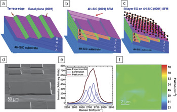
These results clearly demonstrate the importance of understanding and controlling the SiC surface morphology during the EG growth process, in particular reducing or eliminating steps across the entire wafer to promote the highest-performance devices possible. To this end, one of the most promising new research areas is EG growth on step-free mesas (SFMs) on SiC.Reference Nyakiti, Myers-Ward, Wheeler, Imhoff, Bezares, Hayden, Caldwell, Friedman, Matis, Baldwin, Campbell, Culbertson, Eddy, Jernigan and Gaskill64, Reference Bolen, Colby, Stach and Capano65 Growth of large-area (200 × 200 μm2) Bernal-stacked bilayer EG, depicted in Figure 7a–c, on engineered atomically flat 4H-SiC(0001) SFMs was recently demonstrated for the first time.Reference Nyakiti, Myers-Ward, Wheeler, Imhoff, Bezares, Hayden, Caldwell, Friedman, Matis, Baldwin, Campbell, Culbertson, Eddy, Jernigan and Gaskill64 This resulted in the complete elimination of SiC step bunching and a reduction of the heights of EG surface features (not shown) by at least a factor of 50 as compared to those typically found after EG growth on conventional SiC(0001) substrates.
(a–c) Schematic depictions (with an exaggerated vertical scale) of the surface morphologies of (a) a patterned stepped mesa after H2 etching and before homoepitaxial growth of n-doped 4H-SiC, (b) a step-free mesa (SFM) after lateral homoepitaxial growth of the steps to the mesa edge that replicates the underlying tetrahedrally bonded C–Si bilayer stacking sequence of “ACAB” and forms an atomically smooth 4H-SiC surface, and (c) bilayer epitaxial graphene (EG) formation on an SFM. (d) Scanning electron microscopy image of a 200 μm × 200 μm mesa with bilayer EG. (e) Representative Raman 2D band fitted with a set of four Lorentzian functions, confirming the presence of bilayer EG, and (f) map of the Raman 2D-band full width at half-maximum (FWHM) showing uniform bilayer EG. Reproduced with permission from Reference 64. ©2012, American Chemical Society.

Micro-Raman spectroscopy performed on the SFM shown in Figure 7d yielded a 2D band that was fitted with a set of four Lorentzian functions (Figure 7e), confirming the formation of a Bernal-stacked bilayer. A map of the FWHM of the Raman 2D peak showed a fairly uniform bilayer EG coverage across the SFM (Figure 7f). Also, the uniformity and magnitude of the strain in the EG on the SFM approached values for stress-free exfoliated graphene flakes (which typically exist only in much smaller areas) and is comparable to the strain in quasi-free-standing (intercalated) EGReference Speck, Jobst, Fromm, Ostler, Waldmann, Hundhausen, Weber and Seyller66 (discussed at the end of this section). Further, preliminary Hall transport measurement results on large-area bilayer samples were similar to prior reports on bilayer exfoliated flakes. Thus, engineered ultraflat SiC surfaces enable production of regular, Bernal-stacked bilayer EG with areas considerably larger than those reported for bilayer flakes. Developing this approach for wafers could provide a path toward using bilayer graphene in future graphene electronics applications and offer a possible solution to the current limitations imposed by graphene growth on conventional substrates.
Most of the EG growth research to date has utilized nominally on-axis or “conventional” SiC(0001) substrates with off-cuts of 0.8° or less, whereas limited information is available on the impact of substrate orientation on graphene properties or growth mechanism. Initial investigations on forming graphene on 6H-SiC nonpolar planesReference Daas, Daniels, Shetu, Sudarshan and Chandrashekhar67 and on other polytypesReference Ouerghi, Marangolo, Belkhou, El Moussaoui, Silly, Eddrief, Largeau, Portail, Fain and Sirotti68 have only just begun and potentially offer new avenues to exploit. For example, EG growth on nonpolar substrates could provide insight into graphene formation independent of the interface layer (IFL) and the influence of threading screw dislocations (TSDs).
Another area in need of further research is growth on C-face SiC. As discussed previously, when compared to Si-face EG samples, which are only one to a few layers thick, conventionally grown graphene on the C face is thicker and has a more complicated, multidomain morphology. Yet, films of this type are among the most promising candidates for technological applications because of their higher mobility; for example, Hall bars with mobilities of 27,000 cm2 V–1 s–1 for a p-type density of ∼1012 cm–2 have been reported.Reference Tedesco, VanMil, Myers-Ward, McCrate, Kitt, Campbell, Jernigan, Culbertson, Eddy and Gaskill37, Reference Berger, Song, Li, Wu, Brown, Naud, Mayou, Li, Hass, Marchenkov, Conrad, First and de Heer48 Although not completely understood in terms of growth and transport mechanism, the rotationally faulted C-face EG promotes electronic decoupling of graphene sheets from one another in multilayer EG.Reference Hass, Varchon, Millan-Otoya, Sprinkle, Sharma, de Heer, Berger, First, Magaud and Conrad69 Unfortunately, only a handful of investigations have been conducted on the growth and properties of C-face EG, and because graphene formation on the C face is rapid and so readily produces thick films, even fewer studies have probed the interface between the substrate and graphene. A report of single-layer graphene on the C face using a confined geometry recently became availableReference Wu, Hu, Ruan, Madiomanana, Hankinson, Sprinkle, Berger and de Heer70 and points to encouraging properties. Adapting this approach to the wafer scale is the next research step.
Finally, intercalation of EG is an area ripe for additional exploration. Intercalation is the process by which the Si bonds within the IFL are passivated (by hydrogen,Reference Riedl, Coletti, Iwasaki, Zakharov and Starke71 lithium,Reference Virojanadara, Watcharinyanon, Zakharov and Johansson72, Reference Sugawara, Kanetani, Sato and Takahashi73 fluorine,Reference Wong, Huang, Wang, Cao, Qi, Santoso, Chen and Wee74, Reference Walter, Jeon, Bostwick, Speck, Ostler, Seyller, Moreschini, Kim, Chang, Horn and Rotenberg75 etc.), converting the IFL into a free-standing graphene layer. For example, investigations of quasi-free-standing graphene on SiC(0001) prepared by intercalation of hydrogen between the IFL and the SiC substrate have been reported.Reference Speck, Jobst, Fromm, Ostler, Waldmann, Hundhausen, Weber and Seyller66, Reference Riedl, Coletti, Iwasaki, Zakharov and Starke71 This results in a p-type EG layer(s) and can reduce carrier concentration.Reference Riedl, Coletti, Iwasaki, Zakharov and Starke71 Speck et al.Reference Speck, Jobst, Fromm, Ostler, Waldmann, Hundhausen, Weber and Seyller66 achieved carrier mobilities of >3000 cm2 V–1 s–1 at room temperature with corresponding p-type densities in the range of ∼(5.0–6.5) × 1012 cm–2after intercalation. This implies that the intercalated layer is decoupled from the substrate and that only negligible interactions occur, potentially providing a tunable material for electronic devices. Such samples offer an opportunity to study the basic physics of electron transport and the impact of an interface layer (removed by intercalation). Also, transistor development using intercalated graphene for high-frequency applications has shown considerable promise.Reference Lin, Farmer, Jenkins, Wu, Tedesco, Myers-Ward, Eddy, Gaskill, Dimitrakopoulos and Avouris21, Reference Lin, Dimitrakopoulos, Jenkins, Farmer, Chiu, Grill and Avouris61, Reference Lin, Jenkins, Farmer, Valdes-Garcia, Avouris, Sung, Chiu and Ek76
These and other areas of EG research offer great promise for the realization of wafer-scale graphene layers exhibiting near-theoretical properties comparable to those of exfoliated flakes and strongly suggest that sustained progress in the epitaxial graphene field should be expected for the foreseeable future.
Acknowledgments
L.O.N. and V.D.W. acknowledge the support of the American Society for Engineering Education/Naval Research Laboratory Postdoctoral Fellow program. Work at the US Naval Research Laboratory was supported by the Office of Naval Research.