Introduction
In the past decades, self-assembled nanocomposites have become a glamorous research topic because various kinds of fascinating and novel properties and multifunctionalities can be designed via the intercoupling among spin, orbital, charge, and lattice degrees of freedom within the materials.[Reference MacManus-Driscoll1–Reference Ramesh and Spaldin3] Notably in the research field of complex oxides, the applicable functionalities for combination cover almost all application spectra, ranging from metallic, semiconducting, insulating, ferromagnetic, ferroelectric, multiferroic, superconducting, nonlinear optical effects, etc. [Reference Schlom, Chen, Pan, Schmehl and Zurbuchen4] In addition, an important factor that affects the functionalities of composites is the connectivity, defined as the number of dimensions in which the components are self-connected. The possible connectivities can be sorted out in 16 different types: 0–0, 1–0, 2–0, 3–0, 1–1, 2–1, 3–1, 2–2, 3–2, 3–3, 0–1, 0–2, 0–3, 1–2, 1–3, and 2–3. However, the most common schemes, 0–3-type particulate composites, 2–2-type laminate composites, and 1–3-type fiber composites, are able to give rise to the specific anisotropic properties.[Reference Nan, Bichurin, Dong, Viehland and Srinivasan2, Reference Newnham and Trolier-McKinstry5] With the recent advancements in thin-film processes, the self-assembled composites can also be fabricated at nanoscale in a film-on-substrate geometry. Comparing with 2–2-type multilayer films, 1–3-type nanocomposite thin films draw more attention because of the high interface-to-volume ratio and intriguing physical properties. The first successful demonstration of such nanocomposite is the (La0.67Ca0.33MnO3)1−x–(MgO)x composite system on a (100)-oriented MgO substrate by means of the metal organic aerosol deposition method, by Lebedev et al. in 2002.[Reference Lebedev, Verbeeck, Van Tendeloo, Shapoval, Belenchuk, Moshnyaga, Damashcke and Samwer6] When the concentration of MgO exceeds 0.3 (x > 0.3), La0.67Ca0.33MnO3 grains are separated and surrounded by the MgO matrix. A latter work by Moshnyaga et al.[Reference Moshnyaga, Damaschke, Shapoval, Belenchuk, Faupel, Lebedev, Verbeeck, van Tendeloo, Mucksch, Tsurkan, Tidecks and Samwer7] also confirmed that the structural and magnetotransport properties of the La0.67Ca0.33MnO3 nanoclusters can be tuned by the tensile stress originating from the MgO second phase. Nevertheless, one of the most studied systems, recently, is the nanocomposite thin films consisting of perovskite and spinel materials, starting from the pioneering work of spinel CoFe2O4 nanopillars embedded in perovskite BaTiO3 grown on the (001)-oriented SrTiO3 substrate.[Reference Zheng, Straub, Zhan, Yang, Hsieh, Zavaliche, Chu, Dahmen and Ramesh8–Reference Zheng, Zhan, Zavaliche, Sherburne, Straub, Cruz, Chen, Dahmen and Ramesh10] This system exhibits an enhanced and controllable magnetoelectric (ME) coupling, wherein the magnetic property of the nanocomposites can be manipulated by applying an electric field and vice versa. In addition, controllability of intriguing functionalities, such as the enhanced low-field magnetoresistance (LFMR) in (La0.7Sr0.3MnO3)0.5–(ZnO)0.5 vertically aligned nanocomposite (VAN) thin films,[Reference Chen, Bi, Tsai, Lee, Su, Zhang, Jia, MacManus-Driscoll and Wang11] the improved dielectric response in (BiFeO3)0.5–(Sm2O3)[Reference Yang, Wang, Yoon, Wang, Jain, Feldmann, Dowden, MacManus-Driscoll and Jia12]0.5 and the enhanced ferroelectricity in (BaTiO3)0.5 − (Sm2O3)[Reference HarringtonSophie, Zhai, Denev, Gopalan, Wang, Bi, RedfernSimon, Baek, Bark, Eom, Jia, Vickers and MacManus-Driscoll13]0.5 self-assembled vertical heteroepitaxial nanostructures (VHNs), are continuously unveiled. In this review, we emphasize on the development of 1–3-type nanocomposite thin films, or the so-called “self-assembled VHN thin films”, in particular, the systems composed of perovskites and spinels. In the following section, we will first introduce the fabrication of the self-assembled VHN films by the pulsed laser deposition (PLD) process and the corresponding growth mechanisms, which are extensively studied recently. Growth parameters such as temperature, substrate orientation, and strain are very crucial in determining the morphologies and crystal anisotropies of nanocomposites. As the main objective of the growing VHN is to be able to explore the multi-functionalities, we will introduce the approaches to functionality design by three dominant interactions—mechanical, physical, and chemical—case by case along with several recent works that include phenomena such as the ME effect, photomagnetic effect, large magnetoresistance (MR), etc. In the final section, the conclusive concepts will be delineated again and the future directions will be suggested. We genuinely hope that this comprehensive review from growth to design of the nanomaterial systems provide readers an opportunity to understand the magnificence of VHN and further helps to develop innovative designs with the desired properties for practical applications in the future era.
Growth mechanism of self-assembled VHN
Fabrication of the self-assembled VHN films has been successfully synthesized via several techniques such as PLD,[Reference Zheng, Wang, Lofland, Ma, Mohaddes-Ardabili, Zhao, Salamanca-Riba, Shinde, Ogale, Bai, Viehland, Jia, Schlom, Wuttig, Roytburd and Ramesh9, Reference Chen, Bi, Tsai, Lee, Su, Zhang, Jia, MacManus-Driscoll and Wang11, Reference Liao, Tsai, Liang, Liu, Yang, Lin, Lai and Chu14–Reference Aimon, Kim, Choi and Ross16] pulsed electron deposition (PED),[Reference Comes, Khokhlov, Liu, Lu and Wolf17] and chemical solution method.[Reference Lebedev, Verbeeck, Van Tendeloo, Shapoval, Belenchuk, Moshnyaga, Damashcke and Samwer6, Reference Moshnyaga, Damaschke, Shapoval, Belenchuk, Faupel, Lebedev, Verbeeck, van Tendeloo, Mucksch, Tsurkan, Tidecks and Samwer7, Reference Staruch, Hires, Chen, Bi, Wang and Jain18] The main fabrication method focused in this paper is the PLD process. PLD has many advantages, such as precise stoichiometry transfer from target to substrate, fast growth rate, high crystalline quality of film, and versatility of growing a wide range of complex materials, and thus it becomes the most popular tool to develop the nanostructure systems.
The schematics in Fig. 1(a) visually describe the general evolution of self-assembled VHN films consisting of two constituents with different structures from initial to final stages. These selected materials are almost immiscible with each other that can result in spontaneous phase separation. In the very early stage of deposition before the substrate being fully covered with the deposited constituents, the material with higher wetting ability prefers to form lamellas or nanosheets (layer-by-layer growth mode) and the other in less contact with the substrate would form nanoparticles (island growth mode). As these species continue to arrive onto the substrate from target, the material with the layer-by-layer growth mode quickly fills the empty space and limits the growth direction of the nanocrystals along the out-of-plane direction. Finally, the film after the growth exhibits the self-assembled nanostructured thin film with 1–3 phase interconnectivity. This growth dynamics of the self-assembled VHN has been evidenced in the famous example of BiFeO3–CoFe2O4 composites, reported by Zheng et al.[Reference Zheng, Straub, Zhan, Yang, Hsieh, Zavaliche, Chu, Dahmen and Ramesh8] and Hsieh et al.[Reference Hsieh, Kuo, Liao, Liu, Chen, Lin, Chen, Lai, Zhan, Chueh and Chu19] Based on the Winterbottom construction, the CoFe2O4 deposited on the (001)-oriented SrTiO3 substrate has weaker wetting ability than BiFeO3, which leads to the island growth mode for CoFe2O4 and the layer-by-layer mode for BiFeO3.[Reference Zheng, Zhan, Zavaliche, Sherburne, Straub, Cruz, Chen, Dahmen and Ramesh10] The in situ reflective high-energy electron diffraction (RHEED) patterns in Fig. 1(b) show the evolution of CoFe2O4 nanocrystals, with increasing laser pulses from 0 to 18,000, on the (001)-oriented SrTiO3 substrate at 700 °C. The typical diffraction spots of CoFe2O4 nanocrystals, as emphasized by red circles, emerge with weakened streak feature of the SrTiO3 substrate at very early stage of the PLD process about 100–150 pulses, and the mean size of about 8 nm CoFe2O4 particles can be observed on the surface as shown in atomic force microscopy (AFM) images [Fig. 1(c)]. As the deposition process goes on to 18,000 pulses, only the diffraction feature of the CoFe2O4 remains on the RHEED screen. It indicates that CoFe2O4 nanocrystals congregate to become nanopillars embedded in BiFeO3 matrix, and present the morphology of extrusive truncated pyramids that is the equilibrium shape of CoFe2O4 crystal with eight {111} facets [Fig. 1(d)]. The similar observation has been made in the case of SrRuO3–CoFe2O4 system using dual targets PLD process proposed by Liu et al.[Reference Liu, Chen, He, Liang, Chen, Chien, Hsieh, Lin, Arenholz, Luo, Chueh, Chen and Chu15]
(a) Schematic evolution of self-assembled VHN films from initial to final stage. (b) The evolution of CoFe2O4 nanostructures on the SrTiO3 substrate at 700 °C recorded by RHEED patterns with counts of laser pulse from 0 to 18,000. (c) AFM images of CoFe2O4 nanocrystals in 8 nm of mean size (700 °C, 200 pulses). (d) AFM images of CoFe2O4 nanopillars, showing the morphology of extrusive truncated pyramids (700 °C, 18,000 pulses). (b), (c), and (d) are reproduced from Ref. Reference Hsieh, Kuo, Liao, Liu, Chen, Lin, Chen, Lai, Zhan, Chueh and Chu19 by permission of The Royal Society of Chemistry.

Control of nanostructure: size, morphological shape, and crystallographic orientation
Effect of temperature on the size of nanostructures
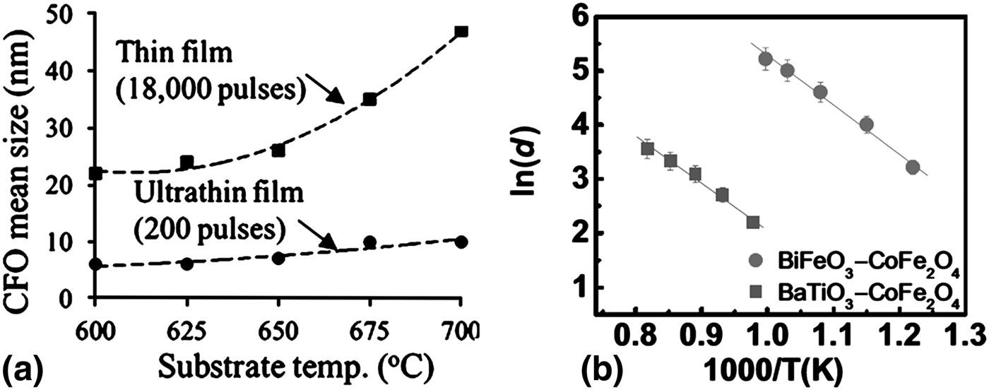
Substrate temperate is an important parameter to control the mean size of self-assembled nanostructures in two-phase composite thin films. Results in Figs. 2(a) and 2(b) obtained from Zheng et al.[Reference Zheng, Straub, Zhan, Yang, Hsieh, Zavaliche, Chu, Dahmen and Ramesh8] and Hsieh et al.[Reference Hsieh, Kuo, Liao, Liu, Chen, Lin, Chen, Lai, Zhan, Chueh and Chu19], respectively, indicate that the formation of the self-assembled nanostructures follows the heterogeneous nucleation and growth theory well. In the initial stage of deposition, the ultrafine crystals can be seen as nuclei and the respective critical radius in the classical nucleation theory is obtained as[Reference Wu20]
(a) Relationships of CoFe2O4 mean size and substrate temperature for thin film (18,000 pulses) and ultrathin film (200 pulses). Reproduced from Ref. Reference Hsieh, Kuo, Liao, Liu, Chen, Lin, Chen, Lai, Zhan, Chueh and Chu19 by permission of The Royal Society of Chemistry. (b) Temperature dependence of BiFeO3–CoFe2O4 and BaTiO3–CoFe2O4 nanostructures grown on (001)-oriented SrTiO3 substrates. Reproduced from Ref. Reference Zheng, Straub, Zhan, Yang, Hsieh, Zavaliche, Chu, Dahmen and Ramesh8 by permission of © 2006 WILEY–VCH Verlag GmbH & Co. KGaA, Weinheim.
 $$r^\ast = - \displaystyle{{2{\gamma _{12}}} \over {\Delta {G_{{\rm het}}}}} = \left({\displaystyle{{2{\gamma _{12}}} \over {\Delta {H_{{\rm het}}}}}} \right)\displaystyle{{{T_{\rm m}}} \over {{T_{\rm m}} - {T_{\rm s}}}} = \left({\displaystyle{{2{\gamma _{12}}{T_{\rm m}}} \over {\Delta {H_{{\rm het}}}}}} \right)\displaystyle{1 \over {1 - {T_{\rm s}}/{T_{\rm m}}}}\comma \;$$
where γ 12 is the interfacial energy between the substrate and CoFe2O4 nuclei; ΔG het and ΔH het are the change in free-energy barrier and enthalpy per unit volume for heterogeneous nucleation, respectively; T m is the melting point of CoFe2O4 (1843 K),[Reference Srinivasan, Rasmussen, Gallegos, Srinivasan, Bokhan and Laletin21] and T S is the surrounding temperature (or substrate temperature). For a small variation of T S/T m (from 0.466 at 600 °C to 0.519 at 700 °C), the critical radius of nuclei is expected to follow an approximately linear dependence with temperature, which is consistent with the results in Fig. 2(a). As the deposition continues, the nuclei that exceed the critical size start to grow, and the crystal size is determined by movement of atoms, which can better be described by the standard two-dimensional (2D) diffusion model[Reference Zheng, Straub, Zhan, Yang, Hsieh, Zavaliche, Chu, Dahmen and Ramesh8]:
 $${d^2} = 4{{\tilde D}_0}\, {e^{ - {{{E_{\rm a}}} / {kT}}}}t = 4{{\tilde D}_0}\, {e^{ - {{{E_{\rm a}}} / {kT}}}}\displaystyle{1 \over \nu }\comma \;$$
where d is the lateral size; is the maximum value of the diffusion constant at infinite temperature; E a is the activation energy; k is the Boltzmann constant; T is the temperature, and t is the diffusion time. Since diffusion is finite within the sample during the deposition, the diffusion time is thus determined by the growth rate (ν = 1/t). The equation can then be simplified as
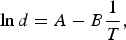 $$\ln d = A - B\displaystyle{1 \over T}\comma \;$$
where A and B are constants, and B = E a/2k. It clearly demonstrates that in steady state the pillar diameter exponentially increases with the substrate temperature, which is consistent with the observed results as shown in Fig. 2(b). Based on these results, we are aware that the formation of nanopillars obeys the theory of nucleation and growth wherein the substrate temperature is a dominant parameter to determine the diffusivity and the final size thereof.
In addition, the post-annealing process also has significant influence on the diffusion behavior. Yan et al. have proposed that the diffusion behavior would change from two dimensions to preferably one dimension when the annealing temperature increases to ~1060 °C in BaTiO3–CoFe2O4 nanocomposite.[Reference Yan, Bai, Li and Viehland22, Reference Yan, Yang, Wang, Xing, Li and Viehland23] When the annealing temperature is high enough (>980 °C), these spinel nanopillars merge into larger ones at the expense of smaller ones and in some regions the belt-shaped nanostructures elongated along the <110> direction appear. Such a high temperature lessens the clamping effect of the substrate and matrix on CoFe2O4, and the results in the fact that CoFe2O4 prefers a ledge growth mechanism, similar to the original growth of spinel single crystal due to a spatial distribution of cations along the <110> direction.
Tailoring morphology and crystallographic anisotropy of the nanostructures by substrate engineering
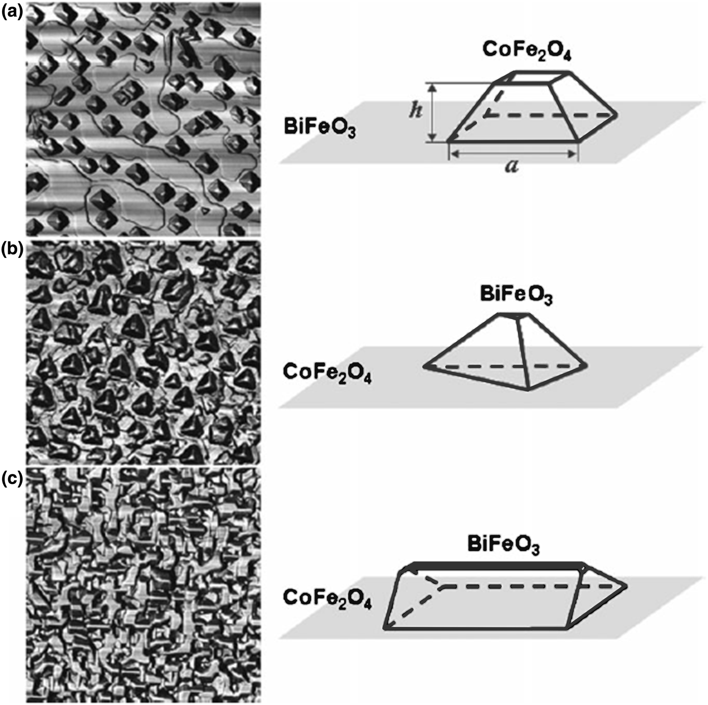
Formation of nanostructures of different sizes can be thought as the consequence of diffusion mechanism, in addition, the morphologies and crystallographic anisotropy can be manipulated by connectivity among the deposited species and substrates, and energetic competition between the respective surfaces and interfaces. According to the Winterbottom construction, at equilibrium, the competition among different surface energy terms dictates the shape and the ability of a particular material to form the nanostructure in the matrix of other material. One of the representative examples is BiFeO3–CoFe2O4 VHN grown on different orientations of SrTiO3 substrates, as shown in Fig. 3.[Reference Zheng, Straub, Zhan, Yang, Hsieh, Zavaliche, Chu, Dahmen and Ramesh8, Reference Zheng, Zhan, Zavaliche, Sherburne, Straub, Cruz, Chen, Dahmen and Ramesh10] Usually, the lowest surface energy in most of the perovskite phases lies on {100} planes, and thus it leads to a cubic equilibrium shape with six {100} facets. In contrast to perovskites, spinels have the lowest surface energy on {111} surfaces, reflected in an equilibrium shape of an octahedron bounded by eight {111} facets. Therefore, on a (001) SrTiO3-oriented substrate, BiFeO3 wets the substrate completely and CoFe2O4 prefers islands bonded by four {111} surfaces in the nucleation stage. As the growth process continues, CoFe2O4 will grow as pillars embedded in a BiFeO3 matrix, which remain the morphology of extrusive pyramids on surface. Conversely, on the (111)-oriented SrTiO3 substrates, CoFe2O4 has more wetting ability than BiFeO3, where BiFeO3 becomes the nanopillars embedded in a CoFe2O4 matrix and the corresponding morphology presents BiFeO3 tetrahedrons with a small (111) end facet on its top and (001), (010), and (100) side facets. On the (110)-oriented SrTiO3 substrate, the wetting abilities of both BiFeO3 and CoFe2O4 phases are close that results in formation of a maze pattern. In this case, BiFeO3 still has a higher surface morphology than CoFe2O4 and forms hut-shaped islands with the (110) end facet and the {100} side facets. Similar conclusion can be drawn in case of the BiFeO3–CoFe2O4 nanocomposites grown on the (001)-oriented MgAl2O4 substrate as proposed by Stern et al. Their result shows that the spinel CoFe2O4 has higher wetting ability than perovskite BiFeO3, and perovskite BiFeO3 becomes nanogrids surrounded by spinel CoFe2O4, while these two materials are deposited on the spinel MgAl2O4 substrate.[Reference Stern, He, Zhou, Silwal, Miao, Vargas, Spinu and Kim24] In these samples, BiFeO3 and CoFe2O4 have the same crystallographic orientation with respect to the orientation of the SrTiO3 substrate, which is a cube-on-cube type of epitaxial relationship. It indicates that the morphological shapes are highly correlated to the crystallographic orientation.
AFM phase-contrast images of BiFeO3–CoFe2O4 nanostructures (volume fraction of 1:1) grown on (a) (001)-, (b) (111)-, and (c) (110)-oriented SrTiO3 substrates. All images are 2.5 µm × 2.5 µm. The schematics show the shape and facets of the islands. On the (001) substrate, CoFe2O4 has a (001) end facet and (111), (111), (111), and (111) side facets. On the (111) substrate, BiFeO3 has a (111) end facet and (001), (010), and (100) side facets. On the (110) substrate, BiFeO3 has a (110) top end facet and (001), (010), (001), and (100) side facets. Reproduced from Ref. Reference Zheng, Straub, Zhan, Yang, Hsieh, Zavaliche, Chu, Dahmen and Ramesh8 by permission of © 2006 WILEY-VCH Verlag GmbH & Co. KGaA, Weinheim.
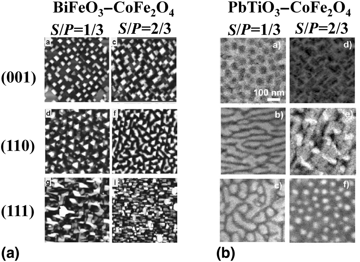
The phase fraction of spinel (x) is another crucial parameter for the morphologies of nanocomposite thin films as well. The same ratio at different pervoskite matrices may lead to different results. Zheng et al.[Reference Zheng, Straub, Zhan, Yang, Hsieh, Zavaliche, Chu, Dahmen and Ramesh8, Reference Levin, Li, Slutsker and Roytburd25] and Levin et al.[Reference Levin, Li, Slutsker and Roytburd25] have demonstrated the morphological changes on several phase fractions in BiFeO3–CoFe2O4 and PbTiO3–CoFe2O4 systems, respectively. As shown in Figs. 4(a) and 4(b), both the systems grown on the (001) SrTiO3 substrate have less change of morphology as the phase fraction varies from 1/3 to 2/3, and CoFe2O4 still remains as the nearly original nanopillars form in either BiFeO3 or PbTiO3 matrix. However, marked discrepancies can be observed between these two systems on (110) and (111) substrates when the phase fraction reverses from 1/3 to 2/3. The morphology of PbTiO3–CoFe2O4 at x = 1/3 starts as an alternating vertical lamellae and labyrinth-like shape while grown on (110)- and (111)-oriented SrTiO3 substrates, respectively, and then converts to irregular-shaped isolated columns of PbTiO3 dispersed in a CoFe2O4 matrix and cylindrical PbTiO3 nanorods in a CoFe2O4 matrix at x = 2/3. The evolution of morphologies is consistent with the results obtained from simulation of phase-field modeling, which describes that the equilibrium arrangements of phases are determined by minimizing the elastic and interfacial energies.[Reference Artemev, Slutsker and Roytburd26] It also suggests that the strain energy between the two phases should be taken into account in addition to the surface energy in some of the self-assembled nanocomposite systems with higher structural coupling.
(a) AFM images of (x) CoFe2O4–(1 − x) BiFeO3 nanostructures with x = 1/3 and 2/3 grown on (001), (111), and (110) SrTiO3 substrates. All images are 3 µm × 3 µm. Reproduced from Ref. Reference Zheng, Straub, Zhan, Yang, Hsieh, Zavaliche, Chu, Dahmen and Ramesh8 by permission of © 2006 WILEY–VCH Verlag GmbH & Co. KGaA, Weinheim (b) SEM images revealing the morphologies of the (x) CoFe2O4–(1 − x) PbTiO3 films grown epitaxially on (001), (111), and (110) SrTiO3 substrates with x = 1/3 and 2/3. The bright and dark regions correspond to PbTiO3 and CoFe2O4, respectively. Reproduced from Ref. Reference Levin, Li, Slutsker and Roytburd25 by permission of © 2006 WILEY–VCH Verlag GmbH & Co. KGaA, Weinheim.
Besides, the use of different kinds of single-crystal substrates, of which the variation of lattice would cause disparity in surface energy, and also provides another means to tune the morphologies and crystallographic orientation of nanostructures. Liao et al. have used (110)o-oriented NdGaO3, (001)c-oriented SrTiO3, and (110)o-oriented DyScO3, where the pseudo-cubic and cubic lattice constants are a pc = 3.85 Å, a c = 3.905 Å, and a pc = 3.94 Å, respectively (c, cubic; pc, pseudo-cubic; o, orthorhombic), to grow the self-assembled BiFeO3 and CoFe2O4 VHN.[Reference Liao, Tsai, Liang, Liu, Yang, Lin, Lai and Chu14] The sample on the (001)-oriented SrTiO3 substrate exhibits the same results as the studies proposed by Zheng et al.[Reference Zheng, Straub, Zhan, Yang, Hsieh, Zavaliche, Chu, Dahmen and Ramesh8, Reference Zheng, Zhan, Zavaliche, Sherburne, Straub, Cruz, Chen, Dahmen and Ramesh10] Interestingly, on the (110)o-oriented [or (001)pc-oriented] DyScO3 and NdGaO3 substrates, BiFeO3 is still a matrix retaining the (001) orientation in the normal direction, but CoFe2O4 exhibits the morphologies of a roof-like islands with (110) orientation and triangle-platform islands with (111) orientation along the surface normal, respectively. These results imply that CoFe2O4 is more sensitive to the interface energy on different perovskite single-crystal substrates than BiFeO3, and therefore, exhibits different morphologies and crystallographic orientations, whereas BiFeO3 retains the same crystallographic orientation on these substrates.
Design of multi-functionalities
After having carefully reviewed the growth and control of VHN systems, we will now turn our attention to the various functionalities of VHN systems. In this part of the review, we shall discuss the three most important interactions, namely, mechanical, physical, and chemical, those lead to novel functionalities. Figure 5 illustrates the schematics of the three main interactions present in VHN systems.
Schematic representation of the three main kinds of interactions happening correspondingly in VHN systems: the mechanical interaction via strain engineering; the physical interaction, such as superconductivity and ferromagnetism; and the chemical interaction by interdiffusion of elements.
Mechanical interaction
Mechanical effect is a derivative of thin-film strain engineering. In strongly correlated oxides, most of the properties are inherently connected to the crystalline structure and strain state; consequently, a subtle compromise of two connected lattices will change the physical properties of the resulting system. Traditionally, the strain state of thin-film heterostructure is determined by the type/nature of the substrate and film thickness. The strain state of the vertical self-assembled nanostructure, on the other hand, is majorly attributed to the lateral lattice mismatch between the pillar and matrix, which can thread through the entire structure, sustaining a stable strain state in the thick film.[Reference MacManus-Driscoll, Zerrer, Wang, Yang, Yoon, Fouchet, Yu, Blamire and Jia27] The mechanical interaction plays a key role in tailoring the physical properties in VHN systems, such as the piezoelectricity–magnetostriction-induced ME effect,[Reference Mathur28–Reference Sun and Kim31] and photostriction–magnetostriction-induced photomagnetic effect.[Reference Liu, Chen, He, Liang, Chen, Chien, Hsieh, Lin, Arenholz, Luo, Chueh, Chen and Chu15]
ME effect induced by elastic coupling
Single-phase multiferroics rely on the coupling of magnetic and electric orders resulting from spin–orbit interaction, which is usually weak, while composite MEs, the combination of magnetostrictive and electrostrictive materials, depend on the interfacial coupling interaction which can overpower the whole system under certain conditions. More so, vertical heterosturcture provides a clamping-free environment by virtue of its lateral geometry enhancing the net ferroelectricity in the system.[Reference Caruntu, Yourdkhani, Vopsaroiu and Srinivasan32–Reference Wu, Gong, Deng and Li35] Theoretical calculations have also evidenced the extraordinary ME response since they possess long-range elastic interaction.[Reference MacManus-Driscoll, Zerrer, Wang, Yang, Yoon, Fouchet, Yu, Blamire and Jia27, Reference Zavaliche, Zheng, Mohaddes-Ardabili, Yang, Zhan, Shafer, Reilly, Chopdekar, Jia, Wright, Schlom, Suzuki and Ramesh36–Reference Landau and Liftshitz38] Therefore, VHN have become promising candidates to build ME response-based devices.
The emergence of VHN architecture has gained increased popularity in the field of oxide heterostructures since Ramesh's group[Reference Zheng, Wang, Lofland, Ma, Mohaddes-Ardabili, Zhao, Salamanca-Riba, Shinde, Ogale, Bai, Viehland, Jia, Schlom, Wuttig, Roytburd and Ramesh9] demonstrated the strong ME coupling by integrating ferroelectric BaTiO3 perovskite and ferromagnetic CoFe2O4 spinel in the form of vertical nanostructures. Soon after this report, nanostructured composites aimed at multiferroic devices are widely studied with combinations of a number of room temperature ferroelectric perovskites [PbTiO3,[Reference Li, Levin, Slutsker, Provenzano, Schenck, Ramesh, Ouyang and Roytburd39, Reference Tsai, Chen, Chang, Tsai, Cheng, Chu, Lai and Hsieh40] Pb(Zr, Ti)O3,[Reference Ren and Wuttig41–Reference Zhang, Fu, Lu, Dai and Chan43] and BiFeO3[Reference Crane, Bihler, Brandt, Goennenwein, Gajek and Ramesh44, Reference Zhan, Yu, Crane, Zheng, Kisielowski and Ramesh45]] and room temperature ferromagnetic spinels (CoFe2O4,[Reference Li, Levin, Slutsker, Provenzano, Schenck, Ramesh, Ouyang and Roytburd39, Reference Tsai, Chen, Chang, Tsai, Cheng, Chu, Lai and Hsieh40, Reference Wan, Wang, Wu, Zeng, Wang, Jiang, Zhou, Wang and Liu42, Reference Zhang, Fu, Lu, Dai and Chan43] NiFe2O4[Reference Ren and Wuttig41, Reference Crane, Bihler, Brandt, Goennenwein, Gajek and Ramesh44, Reference Zhan, Yu, Crane, Zheng, Kisielowski and Ramesh45]). Of particular interest is the assembly of BiFeO3–CoFe2O4 VHN system. From the structural aspect, BiFeO3 and CoFe2O4 are compatible: BiFeO3, with a pseudocubic lattice constant of 3.96 Å, is a room temperature multiferroic compound, exhibiting strong ferroelectric (100 µC/cm2)[Reference Chu, Zhan, Martin, Cruz, Yang, Pabst, Zavaliche, Yang, Zhang, Chen, Schlom, Lin, Wu and Ramesh46, Reference Pabst, Martin, Chu and Ramesh47] and antiferromagnetic behaviors, and CoFe2O4, with a cubic lattice constant of 8.38 Å, is a room temperature ferromagnet. From the chemistry aspect, bismuth and cobalt atoms with large differences in size and chemical properties scarcely react or mix. Hence, this system provides a simple yet decent model to study the kaleidoscope of ME coupling.
Researchers have first grown epitaxial BiFeO3–CoFe2O4 vertical heterostructures on SrTiO3 substrate via PLD,[Reference MacManus-Driscoll, Zerrer, Wang, Yang, Yoon, Fouchet, Yu, Blamire and Jia27] and with the help of scanning probe microscopy (SPM) technique, they have successfully demonstrated the magnetic switching behavior by electric field control (Fig. 6). The strength of ME coupling has been estimated to be ~1.0 × 10⁻² G cm/V, whereas Yan et al. have directly measured the ME coefficient of ~20 mV/cm Oe by a magnetic cantilever method.[Reference Yan, Xing, Wang, Wang, Lei, Li and Viehland48] To inspect deeper, Oh et al.[Reference Oh, Crane, Zheng, Chu, Ramesh and Kim49] have investigated the in-plane and out-of-plane ME susceptibilities (MES) separately by sensitive ME susceptometer equipped with PPMS. They have found that the in-plane MES is about 60 mV/cm Oe which behaves totally different in bulk materials. To apply the concept for practical applications, Zavaliche et al.[Reference Zavaliche, Zhao, Zheng, Straub, Cruz, Yang, Hao and Ramesh50] have found a way to control the selective magnetic configuration by applying the electric field in the BiFeO3–CoFe2O4/SrTiO3 system, and thus mapped out a comprehensive viewpoint for the working principle and controllability of electrically assisted magnetic recording via the SPM technique. Moreover, understanding the fundamentals and mechanism of ME coupling in the BiFeO3–CoFe2O4/SrTiO3 system has become an important issue. There has been tremendous effort, in terms of number of studies to decipher the detailed coupling behavior and mechanism. X-ray magnetic circular dichroism (XMCD) has directly observed the magnetic switching behavior of both Co and Fe in pillars after the electric poling.[Reference Zhao, Scholl, Zavaliche, Zheng, Barry, Doran, Lee, Cruz and Ramesh51, Reference Chen, Hsieh, Liao, Hu, Huang, Kuo, Chin, Uen, Juang, Lai, Lin, Chen and Chu52] This elasticity-induced ME coupling has been then directly proved via high-resolution transmission electron microscopy (HRTEM) and high-resolution x-ray diffraction (HRXRD).[Reference Dix, Muralidharan, Guyonnet, Warot-Fonrose, Varela, Paruch, Sánchez and Fontcuberta53] Dynamics of switching behavior is another key to understand the nature of coupling. The observation of ferroic domain dynamics are recorded and revealed by piezoresponse force microscopy (PFM) and switching spectroscopy PFM (SS-PFM) (Fig. 7). They have conducted a systematic study at BiFeO3, CoFe2O4, and BiFeO3–CoFe2O4 interfaces and found that the switching and electrochemical responses are reduced in the vicinity of interface due to the long-range strain field. It indicates that the switching behavior is inert at the heterostructure interface.[Reference Kalinin, Morozovska, Chen and Rodriguez54, Reference Rodriguez, Jesse, Baddorf, Zhao, Chu, Ramesh, Eliseev, Morozovska and Kalinin55]
Changes in the magnetic response of a (BiFeO3)0.65–(CoFe2O4)0.35 film upon electrical poling. Magnetic force microscopy image taken (a) after magnetization in an upward oriented 20 kOe perpendicular field, and (b) after electrical poling at +12 V along the out-of-plane direction (scale bars, 1 µm). (c) Magnetization measurement taken before (black curves), and after (red curves) electrical poling of 10% of the total film area. (d) Magnified view of M-H loop. Reprinted with permission from Ref. Reference Zavaliche, Zheng, Mohaddes-Ardabili, Yang, Zhan, Shafer, Reilly, Chopdekar, Jia, Wright, Schlom, Suzuki and Ramesh36. © (2005) American Chemical Society.
(a) Topography of multiferroic BiFeO3–CoFe2O4 nanostructures and the corresponding PFM, (b) amplitude, and (c) phase images. The ferroelectric and antiferromagnetic BiFeO3 show a piezoresponse, whereas the ferromagnetic CoFe2O4 spinels show no piezoresponse. (d) SS-PFM map of the work of switching and (e), (f) maps of the positive and negative nucleation biases, respectively. (g) Representative loops from BiFeO3 ( ), CoFe2O4 (
 ), and the BiFeO3–CoFe2O4 heterostructure interface (▼). (h) Fit of the loop shape with coercive and nucleation biases indicated. The work of switching is defined as the area within a loop. Reproduced from Ref. Reference Rodriguez, Jesse, Baddorf, Zhao, Chu, Ramesh, Eliseev, Morozovska and Kalinin55 by permission of IOP Publishing. All rights reserved.
Photomagnetic effect
Besides the ME coupling, mechanically induced interaction has a considerable effect on some of the parameters/functionalities that are available to be part of system design. Another successful example is the combination of photostriction and magnetostriction in SrRuO3–CoFe2O4 vertical heterostructure by Liu et al. in 2012.[Reference Liu, Chen, He, Liang, Chen, Chien, Hsieh, Lin, Arenholz, Luo, Chueh, Chen and Chu15] In principle, photostriction can be understood as an effect coming from the superposition of photovoltage and the converse piezoelectiricity, which has an intrinsic advantage for actuators or sensors applications in the ME noise-free system.[Reference Poosanaas, Tonooka and Uchino56, Reference Uchino and Aizawa57] Lately, ultrafast XRD investigation of SrRuO3 has revealed a large photon-induced strain of 0.5%–1.5% in a time scale of 500 fs laser-pulsed excitation.[Reference Schmising, Bargheer, Kiel, Zhavoronkov, Woerner, Elsaesser, Vrejoiu, Hesse and Alexe58–Reference Schmising, Bargheer, Kiel, Zhavoronkov, Woerner, Elsaesser, Vrejoiu, Hesse and Alexe61] Based on this discovery, the mechanical coupling between optical and magnetic parameters via the vertical heterostructure of SrRuO3 and CoFe2O4 on the SrTiO3 substrate has been demonstrated (Fig. 8). In the SrRuO3–CoFe2O4/SrTiO3 system, the magnetic anisotropy of CoFe2O4 is originally along the vertical direction of pillars; however, the femtosecond-pulsed laser excitation effectively extends the c-axis of SrRuO3, partially relaxing the strain and therefore, the nearly isotropic magnetization results in the non-preferential magnetic domain direction at the same time. At this stage, the change of magnetic anisotropy permits CoFe2O4 magnetic domains to freely select orientation again. This work has introduced a novel approach to perturb magnetic moment orientation with light, which is also achieved by the interplay of epitaxial strain.
(a) AFM topology and (b) MFM image at the same area of a nanostructured SrRuO3–CoFe2O4 sample magnetized by applying a large out-of-plane magnetic field before being illuminated. (c) MFM image at the same area after being illuminated. For convenience, randomly 100 nanopillars are selected to observe the change in magnetization direction. The red circles in (b) are the nanopillars in (a) with downward magnetization, and half of these pillars flipped upward in (c) are presented in yellow circles, suggesting a “liberation” in magnetization during illumination. (d)–(f) Schematic illustrations of the process of magnetic domain flipping during the illumination by ultrafast Ti:sapphire laser pulses—(d) Application of a large out-of-plane magnetic field (7 T) to magnetize all nanopillars downward. (e) Introduction of light on the nanostructured thin film expands the lattice of SrRuO3 and releases the vertical compressive strain of CoFe2O4. (f) Removal of light results in the magnetization of the CoFe2O4 nanopillars to become either parallel or antiparallel to magnetic field direction for the energetically preferred state. Reprinted with permission from Ref. Reference Liu, Chen, He, Liang, Chen, Chien, Hsieh, Lin, Arenholz, Luo, Chueh, Chen and Chu15. © (2012) American Chemical Society.
Physical interaction
Apart from mechanical coupling, there are parameters that interact physically. Explicit examples are phonon–electron coupling in YBa2Cu3O7 and La2/3Ca1/3MnO3 superlattice,[Reference Driza, Blanco-Canosa, Bakr, Soltan, Khalid, Mustafa, Kawashima, Christiani, Habermeier, Khaliullin, Ulrich, Le Tacon and Keimer62, Reference Heinze, Habermeier, Cristiani, Canosa, Tacon and Keimer63] and superconductivity pinning effect in high-temperature superconductors (HTS) based two-phase materials system. Here, we will review some of the recent works on tailoring the functionalities like superconductivity through physical interaction.
Pinning engineering of superconductors
In 1986, the discovery of type-II HTS made superconductivity a popular research field for power applications.[Reference Bednorz and Müller64] However, an issue lies in that the magnetic flux partially retains in material as magnetic fluxons, hindering the supercurrents. Recently, researchers have dug out that the dense existence of pinning centers will largely enhance the critical current, and the approach to reach dense pinning centers is known as pinning engineering.[Reference Larbalestier, Gurevich, Feldmann and Polyanskii65–Reference Matsushita67] Several recent works on pinning engineering have been established parallel so far with the same goal for practical superconducting usage. For example, as shown in Figs. 9(a) and 9(b), Macmanus-Driscoll et al.[Reference MacManus-Driscoll, Foltyn, Jia, Wang, Serquis, Civale, Maiorov, Hawley, Maley and Peterson68] have started the work in 2004 by using structurally and chemically compatible nanoparticle BaZrO3 as the pinning center in YBa2Cu3O7 on single-crystal SrTiO3 and SrTiO3-buffered MgO substrate. YBa2Cu3O7–BaZrO3 samples of different thickness have been viewed and all the samples exhibit a huge enhancement in critical current density (J c) over a wide magnetic field range (~1–5 T). In the same year, Haugan et al.[Reference Haugan, Barnes, Wheeler, Meisenkothen and Sumption69] have synthesized YBa2CuO5 as second phase embedded in YBa2Cu3O7 thin film to enhance J c by a factor of 2. A fine columnar nanostructure of BaZrO3 in YBa2Cu3O7 thin film on biaxially textured substrates has also been carried out by Goyal et al.[Reference Goyal, Kang, Leonard, Martine, Gapud, Varela, Paranthaman, Ijaduola, Specht, Thompson, Chrhten, Pennycook and List70] Other than oxide-based superconductors, pinning engineering has also been investigated in ferropnictide superconductors. Eom's et al.[Reference Lee, Jiang, Zhang, Bark, Weiss, Tarantini, Nelson, Jang, Folkman, Baek, Polyanskii, Abraimov, Yamamoto, Park, Pan, Hellstrom, Larbalestier and Eom71] have successfully implanted vertically aligned second phase into BaFe2As2 via oxides template [Figs. 9(c)–9(e)]. With the aid of dense pinning sites along the c-axis, the irreversibility field (H irr) anisotropy now can be inverted from the a–b plane to vertical plane. Furthermore, the same group consecutively gave a more sophisticated design of the artificial structure shown in Fig. 9(c),[Reference Lee, Tarantini, Gao, Jiang, Weiss, Kametani, Folkman, Zhang, Pan, Hellstrom, Larbalestier and Eom72] which allows large as well as isotropic critical current behavior over a wide angular range. That is, these artificially controlled second phases in a superconductor film modify the functionalities that can be attributed to physical perturbation rather than mechanical or chemical effect.
(a) The example for superconductor with nanoparticle structure; the critical current density measured parallel to c-axis for pure YBa2Cu3O7 (black) and YBa2Cu3O7 + BaZrO3 films (red). (b) The TEM images showing nanoparticle embedded in YBa2Cu3O7 film. (c) is the illustration for the superlattice structure with defects along the c-axis. (d) and (e) are examples for the structure shown in (c); critical current density for SrTiO3 SL [in black, representing (SrTiO31.2 nm/co-doped Ba12213 nm) × (n = 24) superlattice], O–Ba-122 SL [in red, (O–Ba-1223 nm/co-doped Ba12213 nm) × (n = 24) superlattice] and co-doped Ba-122 single layer (in blue). (e) shows the angular dependence of critical current density at 4 T. (a) and (b) are reprinted from Ref. Reference MacManus-Driscoll, Foltyn, Jia, Wang, Serquis, Civale, Maiorov, Hawley, Maley and Peterson68, copyright (2004) and (c)–(e) from Ref. Reference Lee, Tarantini, Gao, Jiang, Weiss, Kametani, Folkman, Zhang, Pan, Hellstrom, Larbalestier and Eom72, copyright (2013) by permission from Macmillan Publishers Ltd: [Nature Materials].
Chemical interaction
Diffusion, which is a representative for mass transportation, is a phenomenon ubiquitously known/existed in the dissimilar-component system.[Reference Callister73] Generally speaking, it is well established that elemental mixing engenders a wide range of modifications depending on the basic properties of host and doped atoms. Chemical interaction discussed in this report infers that the interaction between disparate ions from two distinctive oxides happens in heterostructures, which is based on interdiffusion. It is especially important in strongly correlated systems since the ions strongly interacts with electrons and thereof couples with physical properties.[Reference Dagotto74, Reference Mannhart and Schlom75]
ME coupling induced by chemistry
ME coupling, as discussed earlier, has been on a huge demand in the development of the next generation electronics. However, improvements are often limited by the choices of ferroelectric and ferromagnetic oxides system. Very recently, Liang et al.[Reference Liang, Liu, Liao, Wang, Liu, Lin, Chen, Lai, Borisevich, Arenholz, Li and Chu76] have discovered a large ME effect in ferroelectric/antiferromagnetic vertical heterostructure by means of chemical interaction. They have manipulated the vertical heterostructure of BiFeO3–LiMn2O4 with different concentration ratio to control the degree of Fe doping in LiMn2O4. According to the study, the substitution of Fe for Mn induces the net spin in LiMn2O4,[Reference Hankare, Patil, Sankpal, Jadhav, Mulla, Jadhav and Chougule77] and it has been evidenced by SPM, Auger, and XMCD that in the (BiFeO3)0.66–(LiMn2O4)0.37 system ferroelectricity and ferromagnetism coexist below room temperature [Fig. 10(a)]. ME coupling based on chemical interaction rather than elastic strain is demonstrated by variable field module [Figs. 10(b)–10(d)]. This study gives a decent example for creating new functionality by playing materials chemistry.
(a) The chemical evidence for spin coupling between Mn and Fe ions by XMCD measurement. (b) The ME coupling is measured by variable field module with different magnetic field. The ferroelectric switching response on the application of magnetic field is facilitated as shown in (c) phase hysteresis and (d) amplitude loop. Reproduced from Ref. Reference Liang, Liu, Liao, Wang, Liu, Lin, Chen, Lai, Borisevich, Arenholz, Li and Chu76 by permission of the Royal Society of Chemistry.
MR effect
MR effect, which gave the birth of a new spintronic era, has become a large playground in quantum physics and solid-state physics for decades. Significant MR are usually found in the mixed valence perovskite manganite system with spin polarization in 3d orbitals, described by the double-exchange mechanism.[Reference Zener78] However, the MR effect in single-phase perovskite manganite is observed only in high magnetic field (H = several Tesla).[Reference Jin, Tiefel, McCormack, Fastnacht, Ramesh and Chen79, Reference Snyder, Hiskes, DiCarolis, Beasley and Geballe80] To meet the criteria for practical applications, some works have pointed out that grain boundary in polycrystalline manganite induces spin tunneling and results in the enhancement of MR in relatively low magnetic field (H < 1 T).[Reference Chen, Bi, Tsai, Lee, Su, Zhang, Jia, MacManus-Driscoll and Wang11, Reference Gross, Alff, Büchner, Freitag, Höfener, Klein, Lu, Mader, Philipp, Rao, Reutler, Ritter, Thienhaus, Uhlenbruck and Wiedenhorst81–Reference Hwang, Cheong, Ong and Batlogg83] Taking advantage of heterostructure that includes uniform artificial grain boundary, Liu et al.[Reference Liu, Tra, Chen, Huang, Duan, Hsieh, Lin, Lin, Chen, Ikuhara and Chu84] have obtained an unexpectedly large MR effect in VHN with two non-manganite-based oxides, which is later confirmed resulting from atomic diffusion. As shown in Fig. 11, SrRuO3–CoFe2O4 VHN is demonstrated and they have found that it shows a significant 40% decrease of resistivity in 0.5 T magnetic field about 150 K (Curie temperature of SrRuO3). Authors have pointed out that the key to this abnormal MR is the Fe3+ diffusion, which makes this nanocomposite system present a strong magnetic coupling. A model is also proposed in Fig. 11(c).
(a) The respective MR at 0.5, 1.5, and 3 T exhibit a ~40% decrease of resistivity about 150 K (Curie temperature of SrRuO3). (b) The hysteresis loops measured at different temperatures show an obviously decoupled feature below T C,SrRuO3. (c). The depiction of the cause of large MR in this nanostructure system. The interdiffused Fe ions and CoFe2O4 nanopillars play a role to reduce the resistivity while they are put in a magnetic field. The aligned magnetic moments of Fe ions in SrRuO3 matrix and CoFe2O4 nanopillars result in the suppression of magnetic scattering from ions and interfaces. Reproduced from Ref. Reference Liu, Tra, Chen, Huang, Duan, Hsieh, Lin, Lin, Chen, Ikuhara and Chu84 by permission of © 2013 WILEY–VCH Verlag GmbH & Co. KGaA, Weinheim.
Outlook
So far, many investigations have already pointed out the fantastic physical properties and desired multifunctionalities in the self-assembled VHN films; however, some further directions are still needed to be carried out. First, the creation of various multifunctionalities by coupling of two or more constituent materials may be the faster and more efficient direction than looking for the single-phase materials with the same effect. To understand how many multifunctionalities can be created in self-assembled nanocomposites, we start with five commonly observed intrinsic properties of materials, such as permittivity/conductivity, permeability, elastic constant, specific heat capacity, and optical indices. The corresponding input sources to manipulate these properties are electric field, magnetic field, stress, heat, and light.[Reference Pokropivny and Skorokhod85] By cross-linking these input sources with other controllable properties, the so-called “multifunctionalities” can be obtained as shown in Fig. 12. From this figure, we can find that in addition to the ME effect, photomagnetic effect, and large MR mentioned earlier, it seems that many “intelligent” functions are still being discovered in self-assembled nanocomposite systems through correct design and fabrication.
Obtainable functionalities by cross-linking of the input sources (big circles) with controllable physical properties (small circles). Five commonly available input sources: E, electric field; H, magnetic field; T, heat; L, light or electromagnetic wave; and σ, stress. The corresponding physical properties: P /ρ, permittivity/resistivity; M, permeability; C, specific heat; n, optic indexes; and ε, elastic constants. The so-called “multifunctionalities” means the intrinsic physical properties can be operated by other kinds of input sources.
Second, most of the investigations about the self-assembled VHN films are mainly constructed on the oxides-based systems, for example, perovskites-spinels and perovskites-wurtzites. Different types of oxides can usually have strong structural compatibility with others through the bridge of oxygen atoms, and thus they are easier to form heterointerfaces when interconnected. Interactions across heterointerfaces sometimes carry unusual properties that are definitely worth studying for fundamental understanding, for example, the electrically modulated local conduction at tubular interfaces around the nanopillars in BiFeO3–CoFe2O4 system.[Reference Hsieh, Liou, Huang, Liang, He, Zhan, Chiu, Chen and Chu86] Although oxides have a very broad range of applications, they still have some limitations on physical properties such as electric conductivity, compared to those non-oxides systems. An attempt to grow the self-assembled nanocomposites films combining metals or semiconductors with oxides may be another feasible direction in this field of research for higher practicality. Vidal et al. have successfully demonstrated that the deposition of co-doped CeO2 under special growth condition leads to the reduction of CoO into slanted Co nanowires assembly embedded in CeO2/SrTiO3 (001) epilayers. The sample exhibits interesting magneto-optical properties with rather strong values of the Faraday ellipticity.[Reference Vidal, Schio, Keller, Zheng, Demaille, Bonilla, Milano and de Oliveira87, Reference Vidal, Zheng, Milano, Demaille, Schio, Fonda and Vodungbo88] This is a good instance to confirm the possibility of self-assembled VHN films composed of oxides and non-oxides. Such combinations will extend the self-assembled VHN films into a brand-new area and create more chances for special purposes.
Apart from the scientific investigations, there are some impediments that hinder the realization for practical applications. One is the stochastic distribution of CoFe2O4 pillars in BiFeO3–CoFe2O4 vertical heterostructure. The self-assembled VHN films with ordered arrangement of nanostructures hold great promise for novel applications such as microelectronics, optoelectronics, photonics, and energy storage. How to make nanopillars in controllable and periodic arrangement is an important issue. Currently, using a patterned substrate or pre-treated template such as anodic aluminum oxide (AAO) to create a preferred nucleation site for the formation of nanostructures seems to be the way[Reference Comes, Liu, Khokhlov, Kasica, Lu and Wolf89, Reference Lee, Han, Lotnyk, Schubert, Senz, Alexe, Hesse, Baik and Gösele90] A recent work has overcome the distribution issue intriguingly with the control of lithography patterning method by assistance of focused ion beam (FIB).[Reference Vidal, Zheng, Milano, Demaille, Schio, Fonda and Vodungbo88] The results indeed show a nicely ordered array of BiFeO3–CoFe2O4 vertical heterostructure with high degree control of nanopillar density, which facilitates the future device development. However, the process is arduous to make a large patterned area and takes great effort for preliminary preparation. From this viewpoint, integrating VHN thin film with industrial chain still needs phenomenal breakthrough in the future. Although several concepts have been proposed to functionalize BiFeO3–CoFe2O4 for working devices,[Reference Zavaliche, Zhao, Zheng, Straub, Cruz, Yang, Hao and Ramesh50, Reference Wolf, Jiwei, Stan, Chen and Treger91] the real demonstration is still in urgent need so far.
In VHN architecture, the freedom of growth controllability and functional versatility makes it fascinating and glamorous. Undiscovered phenomena, design of creative functionalities, and industrialization are expected to come up in the near future, leading to scientific contributions and novel applications for the next generation devices.
Acknowledgments
This work was supported by the National Science Council, Republic of China (NSC-101-2119-M-009-003-MY2), Ministry of Education (MOE-ATU 101W961), and Center for Interdisciplinary Science of National Chiao Tung University.