
I. INTRODUCTION
Materials that exhibit enhanced or novel functionalities are essential to the development of a range of technologies, such as energy harvesting and information technology. Heterostructures comprised of materials that exhibit dissimilar yet complementary electrical properties present a new approach to realize novel material functionalities. Key to realizing novel and enhanced functionalities in such composite structures is coupling the electrical properties of the constituent materials.
In this regard, heterostructures comprised of covalently bonded semiconductors and ionic crystalline complex oxides are of particular interest due to the potentially transformative material functionalities that can be realized. Reference McKee, Walker and Chisholm1–Reference Baek and Eom3 Complex oxides exhibit material behaviors that are not found or are difficult to achieve in more traditional semiconductors, such as ferromagnetism, ferroelectricity, metal-insulator transitions, and other strongly correlated phenomena. In contrast, semiconductors exhibit material properties that are difficult to find in oxides, namely, high carrier mobilities at room temperature and direct band-gaps. The dissimilar yet complementary material properties exhibited by semiconductors and complex oxides stem from their respective covalent and ionic natures. Monolithically integrating complex oxides with semiconductors enables their respective properties to be electrically coupled to realize functionalities that cannot be achieved independently in either material alone.
Complex oxides that possess the perovskite structure (ABO3) are nominally lattice matched to the (100) surfaces of diamond cubic or zinc blende structured semiconductors such as Si, Ge, or GaAs, and are thus amenable to monolithic integration. Beyond being amenable to epitaxial growth on semiconductors, perovskite-structured oxides exhibit a broad range of material behaviors. In particular, perovskite oxides in which the B-site cation is a 3d transition metal (e.g., Ti, Mn, Ni, etc.) exhibit rich phase diagrams that can be accessed through substitution of rare-earth and alkaline earth metals on the A-site. Reference Imada, Fujimori and Tokura4 Thus, perovskite complex oxides provide an enormous palette of material behaviors that can be epitaxially integrated on semiconductors.
Heterostructures that integrate the electrical properties of complex oxides with semiconductors could potentially impact a range of emerging technologies. For example, ferroelectric oxides integrated on semiconductors have long been proposed for use in field-effect devices for logic, memory, and sensing applications. Reference Dawber, Rabe and Scott5,Reference Wu and Singh6 In such devices, the re-orientable remnant polarization of the ferroelectric is used to modulate and maintain the surface potential of a semiconducting channel. More recently, the negative capacitance of a ferroelectric gate has been proposed to realize ultra-low power field-effect transistors. Reference Salahuddin and Datta7 Thus, semiconductor-ferroelectric heterostructures could potentially address some of the outstanding challenges encountered in microelectronics. As another example, semiconductors that exhibit a direct band-gap, high carrier mobilities, and high spin-polarization are needed for spintronic and opto-spintronic applications. Reference Zutic, Fabian and Das Sarma8 Realizing a single semiconducting material that intrinsically exhibits high spin-polarization at room temperature has proven challenging. Heterostructures comprised of semiconductors and spin-polarized, half-metallic oxides could provide an alternate spintronic materials platform in which the oxide serves as a source for spin polarized carriers. In the area of energy harvesting, direct band-gap semiconductors that generate electron–hole pairs efficiently under illumination are required for photo-catalysis of water. Semiconductors such as GaAs and other III–V compounds offer direct band-gaps; however, III–V semiconductors have been found to photocorrode under catalytic conditions. Reference Khaselev and Turner9 In contrast, oxide semiconductors are generally robust against photocorrosion; however, their typical indirect and large band-gaps prevent efficient generation of electron–hole pairs. Heterostructures comprised of semiconductors and oxides could mutually address the shortcomings of both materials by providing a platform in which electron–hole pairs photo-generated in the semiconductor are transferred to the oxide surface for reaction. Reference Hu, Shaner, Beardslee, Lichterman, Brunschwig and Lewis10,Reference Ji, McDaniel, Wang, Posadas, Li, Huang, Lee, Demkov, Bard, Ekerdt and Yu11
In the examples discussed above, electrically coupling the complex oxide to the semiconductor is essential to achieve the desired material functionality. Electrical coupling requires that polarization, spin, and charge degrees of freedom be coupled across interfaces within semiconductor–complex oxide heterostructures. The pioneering work of McKee et al. enabled single crystalline SrTiO3 to be grown on semiconductors with atomically abrupt and structurally coherent interfaces using oxide molecular beam epitaxy (MBE). Reference McKee, Walker and Chisholm1 The achievement of single crystalline growth of complex oxides on semiconductors with coherent interfaces is an essential first step to realize electrical coupling between the materials. Beyond epitaxial growth, control of both the physical and the electronic structure of semiconductor–complex oxide heterostructures is essential to control electrical coupling between the two materials. Here we discuss how composition of the A- and B-site cations within the perovskite structure can be exploited to engineer strain and band alignment in semiconductor–complex oxide heterostructures. In the case of A-site composition, we discuss how Sr substitution can be exploited to engineer strain in BaTiO3/Ba1−x Sr x TiO3 (BTO/BST) grown on Ge to enable coupling of the ferroelectric polarization to the semiconductor. Reference Ngai, Kumah, Ahn and Walker12 In the case of B-site composition, we discuss how Zr content can be exploited to control band alignment between SrZr x Ti1−x O3 (SZTO) and Ge. Reference Moghadam, Ahmadi-Majlan, Shen, Droubay, Bowden, Chrysler, Su, Chambers and Ngai13 Analogous to band gap engineering at heterojunctions between compound semiconductors, the control of band alignment at semiconductor–complex oxide interfaces enables control of electrical coupling.
II. PHYSICAL STRUCTURE: ENGINEERING STRAIN IN SEMICONDUCTOR–OXIDE HETEROSTRUCTURES
The properties of complex oxides are strongly coupled to the physical structure of the lattice, and thus altering the lattice through epitaxial strain is an effective way to control material behavior. Reference Rondinelli, May and Freeland14 Epitaxial strain has been exploited to enhance ferroelectricity in BaTiO3, control magnetic properties in manganites, and tune metal-insulator transitions in rare earth nickelates. Reference Choi, Biegalski, Li, Sharan, Schubert, Uecker, Reiche, Chen, Pan, Gopalan, Chen, Schlom and Eom15,Reference Takamura, Chopdekar, Arenholz and Suzuki16,Reference Prellier, Rajeswari, Venkatesan and Greene17,Reference Meyers, Middey, Kareev, van Veenendaal, Moon, Gray, Liu, Freeland and Chakhalian18 Tuning material behavior through strain in heterostructures comprised of complex oxides and semiconductors would be ideal in this regard. For films that are below the critical thickness for relaxation, strain is imparted from the mismatch in lattice constants between the complex oxide film and semiconductor, similar to other epitaxial film-substrate systems. Reference Matthews and Matthews19 However, in contrast to typical epitaxial film-substrate systems, relaxed films of complex oxides grown on semiconductors can still experience tensile strain arising from the mismatch in thermal expansion coefficients between the two materials. The tensile strain is imparted from the semiconducting substrate to the oxide film, since the former contracts far less than the latter as both are cooled to room temperature after growth. Depending on the material system and the intended application, tensile strain arising from differences in thermal expansion may be desirable.
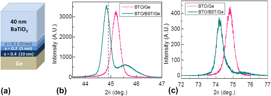
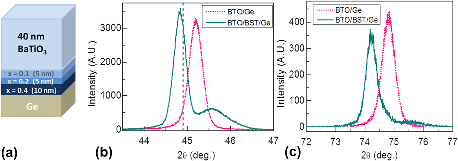
However, tensile strain can also give rise to changes in physical structure that adversely affect electrical coupling between complex oxides and semiconductors. Ferroelectric BTO grown on Ge serves as a prototypical example. For applications involving ferroelectric-semiconductor heterojunctions, the polarization of the ferroelectric is typically intended to manipulate carriers in the semiconductor; thus, a polarization that points predominantly out of the plane of the ferroelectric film is necessary. In addition, the longer screening lengths associated with semiconducting substrates requires that the ferroelectric films to be thick to offset the effects of depolarization fields. Reference Reiner, Walker, McKee, Billman, Junquera, Rabe and Ahn20,Reference Chandra, Littlewood, Rabe, Ahn and Triscone21 However, maintaining an out-of-plane polarization in thick, relaxed films of BTO grown on Ge is challenging, due to the tensile strain imparted by the Ge. For example, Fig. 1(b) shows X-ray diffraction data of a 60 nm thick BTO film (pink dashed curve) grown on Ge, indicating a-axis oriented growth associated with an in-plane polarization. Details on growth procedures for the BTO on Ge using oxide MBE can be found elsewhere. Reference Ngai, Kumah, Ahn and Walker12
(a) Schematic of the BaTiO3/Ba1−x Sr x TiO3 heterostructure grown on Ge. (b) X-ray diffraction data for the Sr-alloyed heterostructure (turquoise solid) shown in (a). The larger (smaller) peak at 2θ = 44.8° (46.1°) arises from the BaTiO3 (Sr alloyed) layer(s). For comparison, the (002) of bulk BaTiO3 2θ = 44.9° (vertical gray dashed) is shown. In the absence of Sr alloying, BaTiO3 grown on Ge is a-axis oriented, as shown by the (200) diffraction peak of a 60 nm thick BaTiO3 film on Ge (pink dotted). (c) (103) peak of the Sr-alloyed heterostructure (turquoise solid) and (301) peak of the non-alloyed BaTiO3 on Ge (pink dotted).
To achieve an out-of-plane polarization, i.e., c-axis oriented growth, a method to apply compressive strain to the BTO film is necessary to offset the tensile strain from the substrate. The introduction of an intermediary buffer layer which has a smaller in-plane lattice constant than BTO has been found to be an effective approach to apply compressive strain. For example, a layer of Ba0.7Sr0.3TiO3 or SrTiO3 is sufficient to enable c-axis oriented growth of BTO on Si and Ge and GaAs. Reference Vaithyanathan, Lettieri, Tian, Sharan, Vasudevarao, Li, Kochhar, Ma, Levy, Zschack, Woicik, Chen, Gopalan and Schlom22–Reference Contreras-Guerrero, Veazey, Levy and Droopad24 For growth on Ge substrates, we execute a variation of the single layer buffer approach by growing a graded structure comprised of 4 layers, with increasing Sr content x (i.e., A-site substitution) for the layers approaching the Ge substrate, as illustrated in Figs. 1(a). Reference Ngai, Kumah, Ahn and Walker12 The first layer is intended to be fully relaxed with respect to the semiconducting substrate and is thus typically thicker and of a larger lattice mismatch with the substrate than the subsequent layers. In contrast to the single layer buffer with a uniform composition, the graded composition enables strain to be applied to very thick films grown on top; furthermore, the strain can be tuned, as shown below.
X-ray diffraction measurements taken on the heterostructures confirm c-axis oriented growth. Figure 1(b) shows X-ray intensity versus 2θ for a typical BTO/BST/Ge heterostructure (turquoise curve). The smaller (002) peak at 45.6° arises from the 20 nm thick Sr alloyed layers near the interface, while the larger (002) peak located at 44.8° is associated with the 40 nm thick BTO top layer. For comparison, the (002) associated with bulk BTO is indicated by the dashed gray line. We note that the compressive strain induced by the Sr alloying enhances the out-of-plane lattice constant of our BTO films to exceed the bulk value. Figure 1(c) shows the (103) (turquoise solid) and (301) (pink dotted) peaks for the BTO/BST/Ge and BTO/Ge heterostructures, respectively. Analysis of the X-ray data for the BTO/BST/Ge heterostructure indicates the average in-plane lattice constant is 3.987 Å.
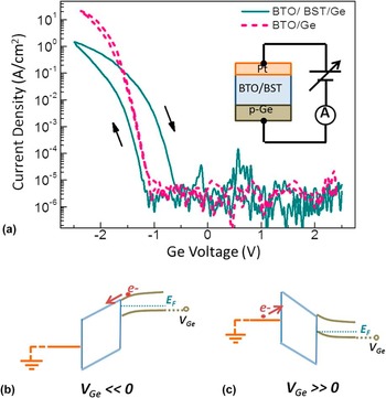
Though ideally the metal/BTO/BST/Ge heterostructure should behave as a capacitor in which charge transport is inhibited, we find instead diode-like behavior due to the near alignment of conduction bands between the ferroelectric and semiconductor, as shown in Fig. 2(a). The rectifying behavior arises from the asymmetry of the metal/ferroelectric/semiconductor heterostructure, namely the presence (absence) of a potential barrier at the Pt/BTO (BST/Ge) interface. For voltages applied to the Ge (V Ge) wafer that are V Ge < −1 V, carriers flow from Ge to Pt electrodes via the BST conduction band, as illustrated in Fig. 2(b). In contrast, for V Ge > −1 V, a barrier arising from the work function of Pt inhibits carriers from entering the BTO conduction band, as illustrated in Fig. 2(c).
(a) Current–voltage characteristics of a BaTiO3/Ba1−x Sr x TiO3/Ge heterostructure (turquoise) and a BaTiO3/Ge heterostructure (pink dashed), which have c-axis and a-axis orientations, respectively. The former exhibits (does not exhibit) hysteresis due to coupling (non-coupling) of the re-orientable polarization to the Ge. The inset shows the geometry of leakage current measurements. (b) Band diagrams illustrating the emergence of rectifying behavior in Pt/BaTiO3/Ba1−x Sr x TiO3/Ge heterostructures. For V Ge < −1 V, charge transport is enabled due to alignment of BaTiO3/Ba1−x Sr x TiO3 and Ge conduction bands. (c) For V Ge > −1 V, charge transport is inhibited by the barrier between Pt and the BaTiO3 conduction band (Reproduced from Ref. Reference Ngai, Kumah, Ahn and Walker12, with the permission of AIP Publishing).

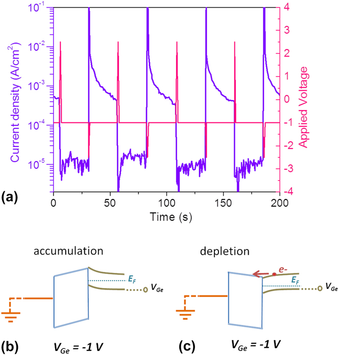
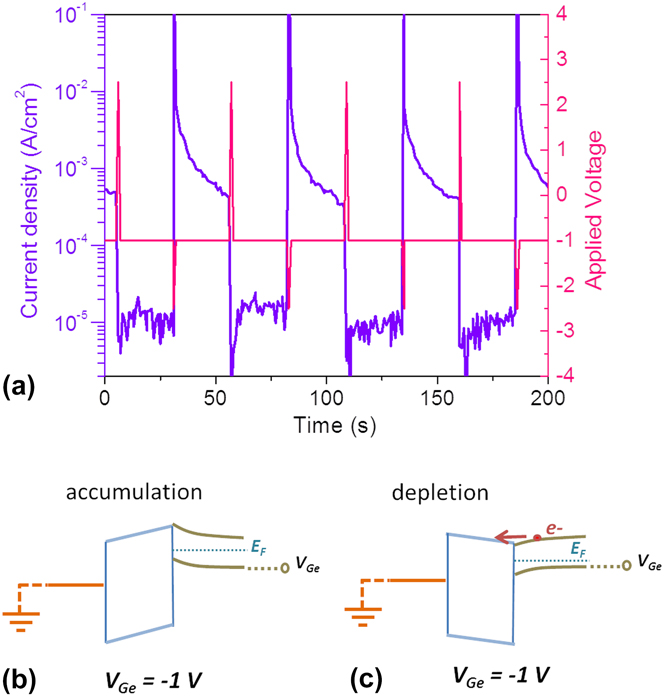
Despite the leakage current, coupling of the re-orientable polarization to the Ge electrode is demonstrated through the observation of hysteretic (non-hysteretic) behavior for the c-axis (a-axis) oriented heterostructures. The hysteretic (non-hysteretic) behavior in leakage current for the c-axis (a-axis) oriented samples is consistent with switching (non-switching) under applied electric fields that are co-linear (perpendicular) to the direction of the polarization. In essence, the Schottky barrier height at the interface between BTO/BST and Ge is modulated between high and low leakage configurations as the ferroelectric polarization is switched, as illustrated in Figs. 3(b) and 3(c). Reference Klein and Chen25,Reference Wen, Li, Wu, Li and Ming26 The modulation of the Schottky barrier height can be exploited to switch the leakage current between high and low leakage regimes by short voltage pulses through the Pt/BTO/BST/Ge stack, as shown in Fig. 3(a). The change in transport current in response to pulsed voltages initially spans over 3 orders of magnitude but decays with time. In this regard, carriers injected through the BTO/BST heterostructure enable exploration of the interplay between ferroelectric and semiconducting properties of ferroelectrics. Reference Fridkin27,Reference Okatan, Mantese and Alpay28
(a) Transport current through a Pt/BaTiO3/Ba1−x Sr x TiO3/Ge heterostructure (violet) versus time as a function of applied voltage (pink). (b) and (c) Band diagrams illustrating two orientations for the polarization and the associated barrier heights for carrier transport for V Ge = −1 V. The state of near inversion in (c) promotes transport of minority carriers through the ferroelectric stack. In contrast, the state of accumulation in (b) forms a barrier for the transport of minority carriers through the ferroelectric stack (Reproduced from Ref. Reference Ngai, Kumah, Ahn and Walker12, with the permission of AIP Publishing).
The coupling of the polarization in c-axis oriented structures demonstrates that structure has a profound impact on electrical coupling within semiconductor–complex oxide heterostructures, and that strain plays a pivotal role in determining structure. Bi-axial tensile and compressive strain is typically imparted to epitaxial complex oxide thin films and heterostructures through growth on single crystal oxide substrates that have larger or smaller lattice constants, respectively. However, for growth of complex oxides on semiconductors, engineering strain by varying the semiconducting substrate is in most cases not a practical option. Applications typically require use of a particular semiconducting substrate; furthermore, integration on an established technology platform such as Si is generally desired. In this regard, engineering strain through compositional grading provides an alternate approach that can, in principle, be generalized to a variety of oxide materials and semiconducting substrates. In addition, the approach of engineering strain through compositional grading provides a method to fine-tune the strain applied to complex oxides grown on semiconductors. For example, Fig. 4(a) shows X-ray diffraction data of BTO/BST/Ge heterostructures in which the Sr content within the graded layers is varied. As Sr content is increased, both the in-plane and out-of-plane lattice constants of the graded BST layers decrease. The reduction of the latter with Sr content is manifested by a shift of the averaged BST peak to higher 2θ values, as shown in Fig. 4(a). In contrast, a concomitant enhancement of the out-of-plane lattice constant of BTO is observed, which is manifested by a shift in the BTO peak position to smaller 2θ values, as shown more clearly in Fig. 4(b), with the corresponding lattice constants summarized in Fig. 4(c). The ability to tune the strain applied to complex oxide films through compositional grading is analogous to growth on various oxide substrates that differ in lattice constant. Here, we have demonstrated how control of compositional grading can be exploited to tune compressive strain. In principle, control of compositional grading can also be used to tune tensile strain, which could further augment the tensile strain imparted by the Ge substrate due to its smaller thermal expansion coefficient.
(a) Tuning of compressive strain through Sr content in a graded buffer. As Sr content x in the first layer of the graded buffer is increased, the out-of-plane lattice constant of the BaTiO3 grown on top is enhanced. The larger (smaller) peak on the left (right) is associated with the BaTiO3 (Ba1−x Sr x TiO3 graded buffer) layer(s). (b) Closer view of the BaTiO3 peak as a function of Sr content in the bottom most layer of Ba1−x Sr x TiO3. (c) The corresponding c-axis lattice constant of the BaTiO3.

Although coupling of the polarization to the semiconductor is demonstrated, the charge transport across the interface between BTO/BST and Ge prevents the dielectric stack from functioning as a capacitor, which is envisioned for the majority of device applications. Thus, control of the electronic structure of the interface, namely band alignment, is also essential to achieve the desired electrical coupling. In the following section we discuss how composition of the B-site cation within the perovskite structure can be exploited to tune band alignment at semiconductor–complex oxide interfaces.
III. ELECTRONIC STRUCTURE: TUNING BAND ALIGNMENT AT SEMICONDUCTOR–CRYSTALLINE OXIDE INTERFACES
The control of band alignments at interfaces between semiconductors and complex oxides is essential to control electrical coupling between the two materials. For AeTiO3 (Ae = Sr, Ba) grown on Si, Ge, or GaAs, band offset measurements indicate the conduction band of the oxide is nearly aligned or below the conduction band of the semiconductor, i.e., type-II. Reference Robertson29–Reference Kornblum, Morales-Acosta, Jin, Ahn and Walker33 Aligned conduction bands or type-II band alignment facilitate charge transport across the interface from the semiconductor to the oxide, and are thus useful for applications such as photocathodes for water splitting, which have been recently demonstrated. Reference Ji, McDaniel, Wang, Posadas, Li, Huang, Lee, Demkov, Bard, Ekerdt and Yu11 However, coupling ferroelectric polarization requires a type-I band offset, in which the conduction band of the oxide is above the conduction band of the semiconductor.
Here we discuss how the band alignment can be tuned continuously from type-II to type-I through B-site substitution of Ti for Zr in solid solution SrZr x Ti1−x O3 (SZTO). In essence, we adapt an approach used to control band offsets at heterojunctions between III–V semiconductors, such as Al x Ga1−x As/GaAs, to semiconductor-complex oxide heterojunctions. Reference Capasso34 The end members of the SZTO solid solution are SrTiO3 and SrZrO3, which have band gaps of 3.2 and 5.6 eV, respectively. Reference Schafranek, Baniecki, Ishii, Kotaka, Yamanka and Kurihara35 For SrTiO3 (SrZrO3), the conduction band is comprised predominantly of Ti 3d (Zr 4d) orbitals that are hybridized with oxygen 2p orbitals. According to Vegard’s law, tuning of the band gap to values between the end members can be achieved by controlling the Zr content in SZTO. Reference Kajdos, Ouellette, Cain and Stemmer36
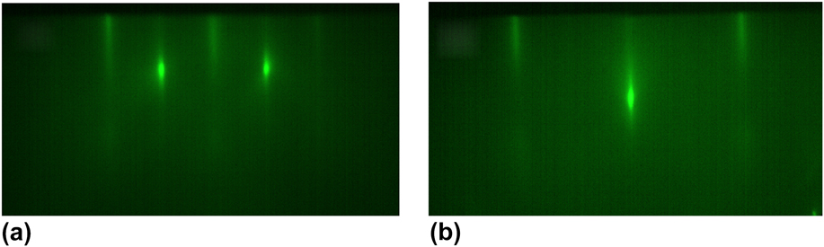
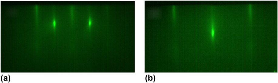
The growth of high quality single crystalline SZTO films on Ge using oxide MBE can be achieved by adopting the technique developed by McKee et al. Reference McKee, Walker and Chisholm1 This technique involves the deposition of a half-monolayer of Sr metal on the (100) surface of Ge to passivate and minimize the formation of GeO x upon subsequent exposure to oxygen. Following the Sr deposition, 2.5 unit cells of SZTO are deposited amorphously at room temperature followed by crystallization at high temperatures through annealing in ultra-high vacuum. Thus far, oxides that exhibit relatively low crystallization temperatures, such as AeTiO3 (Ae = alkaline earth metal Sr, Ba, Ca) and SrHfO3, have been successfully crystallized directly on semiconductors using McKee’s approach. Reference Rossel, Mereu, Marchiori, Caimi, Sousa, Guiller, Siegwart, Germann, Locquet, Fompeyrine, Webb, Dieker and Seo37 We find that zirconate-based SZTO also readily crystallizes at relatively low temperatures on Ge, as shown by the reflection high energy electron diffraction (RHEED) images in Fig. 5 of 2.5 unit-cells of SZTO. Further details on the growth procedure can be found elsewhere. Reference Moghadam, Ahmadi-Majlan, Shen, Droubay, Bowden, Chrysler, Su, Chambers and Ngai13
(a) Reflection high energy electron diffraction (RHEED) images of 2.5 unit cells of SrZr x Ti1−x O3 crystallized on Ge taken along the [Reference Hu, Shaner, Beardslee, Lichterman, Brunschwig and Lewis10] and (b) [Reference Chandra, Littlewood, Rabe, Ahn and Triscone21] directions at 575 °C.
X-ray diffraction measurements confirm single crystalline growth of SZTO on Ge. Figure 6(a) shows survey scans of SZTO films that are ∼15 nm thick of various Zr content x. The unit cell expands along the c-axis with increasing Zr, as indicated by a shift in the (002) peak, which is summarized in Fig. 6(b). The surfaces of films of higher Zr content, which are better lattice matched to Ge, are typically smoother than films with less Zr, as evidenced by enhanced finite thickness fringes in the case of the former. Imaging of the films of higher x using atomic force microscopy quantifies the surface roughness as <1 nm, as shown in Fig. 6(e). The full-width-at-half-max (FWHM) of rocking curves taken on our films are Δω ≈ 0.39° for higher x, as shown in Fig. 6(c). The films remain largely strained to the Ge substrate for higher x, as shown in the direct space map of Fig. 6(d) of an x = 0.65 film. Since the perovskite unit-cell of SZTO is rotated 45° with respect to the diamond-cubic unit cell of Ge, the lattice parameters of the former have been multiplied by
 $\sqrt 2$
to enable comparison on the same plot. The tetragonal structure observed in our x = 0.65 film is expected, given that the end members of solid solution SZTO, namely SrTiO3 and SrZrO3, are cubic and orthorhombic, respectively.
(a) Survey scan of SrZr
x
Ti1−x
O3/Ge heterojunctions for various Zr content x. (b) A shift in the (002) peak is observed with increasing Zr content, indicating enhancement of the out-of-plane lattice constant. (c) Typical rocking curve width of a SrZr
x
Ti1−x
O3 film grown on Ge. (d) Direct-space map of an x = 0.65 SrZr
x
Ti1−x
O3 film on Ge obtained by measuring the (103) and (224) reflections of the former and latter, respectively. The lattice constants of SrZr
x
Ti1−x
O3 have been multiplied by
 $\sqrt 2$
to enable direct comparison with diamond cubic Ge. (e) Atomic force microscopy image of a x = 0.7 SrZr
x
Ti1−x
O3 film grown on Ge, showing <1 nm surface roughness.

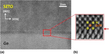
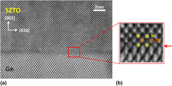
Scanning transmission electron microscopy provides spatially resolved analysis of the interfacial structure between SZTO and Ge. Figure 7(a) is a high-angle annular dark field (HAADF) image of an x = 0.70 film, showing the abruptness of the heterojunction and absence of extended interfacial layers comprised of amorphous GeO x . Figure 7(b) shows a close-up view of the atomically abrupt and structurally coherent interface. Also noteworthy is the nearly equal intensity for the columns in the A- and B-site cation planes, which is due to the closely matched atomic numbers of Sr and Zr.
(a) High angle annular dark field image of an epitaxial x = 0.7 SrZr x Ti1−x O3 film grown on Ge, showing an abrupt interface free of secondary GeO x phases. (b) Closer view of the interface (red arrow) showing atomic registry between the SrZr x Ti1−x O3 and Ge. Sr and Zr/Ti atoms are highlighted in yellow and orange, respectively.

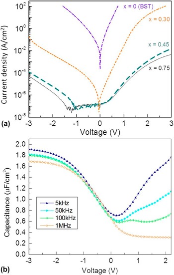
Having shown that single crystalline SZTO can be epitaxially integrated on Ge with atomically abrupt interfaces, we now turn to the results of electrical characterization measurements, which demonstrate the practical outcome of tuning the band offset. Figure 8(a) shows current–voltage measurements through the SZTO/Ge heterojunctions, where the bias is applied to a Ni electrode deposited on top of the SZTO. Current–voltage measurements of an equivalently thick 38 u.c. (∼15 nm) Ba0.4Sr0.6TiO3 (BST) film are also shown, which acts as an x = 0 reference. As the Zr content x increases, a monotonic suppression in leakage current over several orders of magnitude is observed, consistent with the development of a type-I band offset. The asymmetry in the current–voltage characteristics observed about zero-bias for SZTO/Ge and BST/Ge heterojunctions is attributed to a difference in barrier heights for gate and substrate injection. Reference Jeon, Walker, Billman, McKee and Hwang38
(a) Leakage current–voltage characteristics of a 38 u.c. thick SrZr x Ti1−x O3/Ge heterojunction and a 38 u.c. thick Ba0.4Sr0.6TiO3/Ge heterojunction. A monotonic suppression of leakage over several orders of magnitude is observed with increasing Zr content x in the heterojunctions. (b) Capacitance–voltage characteristics of a SrZr x Ti1−x O3/Ge heterojunction (x = 0.70). Bias voltage is applied to a Ni electrode.

The type-I band offset enables SZTO/Ge heterojunctions of high x to behave as metal-oxide-semiconductor capacitors. Capacitance–voltage measurements of an x = 0.70 SZTO/Ge heterojunction are shown in Fig. 8(b) as a function of frequency. The upturn in capacitance at lower frequencies indicates inversion has been achieved in our p-type Ge substrates. We estimate the dielectric constant of the SZTO to be κSZTO = 29, based on the capacitance in accumulation at 1 MHz (i.e., 1.7 × 10⁻⁶ F/cm2). The value of κSZTO = 29 is near the dielectric constant of bulk SrZrO3 (∼30), and is comparable to some of the highest dielectric constants among gate materials that have been reported for Ge. In this regard, crystalline SZTO can potentially be used as a gate dielectric for next-generation field-effect transistors in which high mobility channel materials, such as Ge, are needed. Reference Wallace, McIntyre, Kim and Nishi39
High-resolution core-level (CL) and valence band (VB) XPS measurements on an x = 0.65 film were performed to verify and quantify the band offsets. We use a combination of CL and VB spectra for thin and thick film samples to determine the VB offset (VBO), following a similar procedure used in prior measurements of SrTiO3/Si(001) heterojunctions. The Sr 3d and Ge 3d peaks are used because they are intense and do not overlap appreciably with either XPS or Auger peaks from other elements present, with the exception of the Ge 3d and Zr 4p binding energies. However, for the 6 u.c. films, the Zr 4p is sufficiently weak that it does not affect the more intense Ge 3d line shape or binding energy in a measurable way. The results are shown in Fig. 9. The energy from the top of the VB to the Sr 3d
5/2 core peak,
 ${( {{E_{{\rm{Sr}}\,3{d_{5/2}}}} - {E_{\rm{V}}}} )_{{\rm{SZTO}}}}$
, is measured to be 130.59(6) eV for the 38 u.c. film. Combining this quantity with an analogous energy difference for clean p-Ge(001),
 ${( {{E_{{\rm{Ge}}\,3{d_{5/2}}}} - {E_{\rm{V}}}} )_{{\rm{Ge}}}} = 29.30(4)$
eV, and the CL binding energy difference for the 6 u.c. heterojunction,
 ${( {{E_{{\rm{Sr}}\,3{d_{5/2}}}} - {E_{{\rm{Ge}}\,3{d_{5/2}}}}} )_{{\rm{HJ}}}} = 104.27(2)$
eV, yields a VBO given by
 $\Delta {E_{\rm{V}}} = {( {{E_{{\rm{Sr}}\,3{d_{5/2}}}} - {E_{{\rm{Ge}}\,3{d_{5/2}}}}} )_{{\rm{HJ}}}} + {( {{E_{{\rm{Ge}}\,3{d_{5/2}}}} - {E_{\rm{V}}}} )_{{\rm{Ge}}}} + {( {{E_{{\rm{Ge}}\,3{d_{5/2}}}} - {E_{\rm{V}}}} )_{{\rm{SZTO}}}} = 2.98(8)$
.
Reference Kraut, Grant, Waldrop and Kowalczyk40,Reference Kraut, Grant, Waldrop and Kowalczyk41
Based on the band gap of SrZrO3 and on the premise that the band-gap of SZTO obeys Vegard’s law, the conduction band offset for x = 0.65 is estimated to be 1.2(1) eV.
Reference Schafranek, Baniecki, Ishii, Kotaka, Yamanka and Kurihara35
(a) Core-level and valence band X-ray photoemission spectra taken on 6 u.c. thick (top) and 38 u.c. thick (bottom) x = 0.65 SrZr x Ti1−x O3/Ge heterojunctions. Solid lines are fits to the data. (b) Band diagram showing conduction and valence band offsets for an x = 0.65 SrZr x Ti1−x O3/Ge heterojunction.

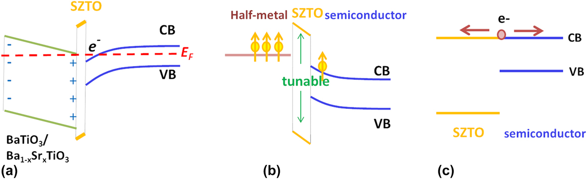
A tunable band offset enables SZTO to act as an electrical platform for coupling the polarization, spin, and charge degrees of freedom of complex oxides to traditional semiconductors. For ferroelectrics, SZTO could serve as an intermediate layer to inhibit charge transfer from a ferroelectric to a semiconductor, thus enabling a capacitor to form in which the polarization of the former maintains accumulation or inversion in the latter, as illustrated in Fig. 10(a). The relatively high-κ of SZTO would reduce the effects of depolarization fields in the ferroelectric in comparison to low-κ intermediary buffer layers such as SiO2 and Si3N4, which have been used in the past. Reference Han and Ma42 For spintronic applications, SZTO could serve as a tunnel barrier through which spin-polarized carriers from a crystalline half-metallic oxide could be injected into a semiconductor, as shown in Fig. 10(b). Injection via tunneling mitigates the large conductivity mismatch between the metallic ferromagnetic oxide and semiconductor, thereby enabling more efficient injection. Reference Zutic, Fabian and Das Sarma8 Furthermore, the barrier height of SZTO is adjustable through control of Zr content, which could greatly enhance injection efficiencies. As a candidate tunnel barrier, SZTO is single crystalline, which could also potentially enhance injection efficiency. Finally, the tunable offset can also facilitate charge transport from the semiconductor to the oxide and vice versa, by enabling conduction bands to be aligned, as illustrated in Fig. 10(c). Charge transport across the interface could potentially be useful in photocatalytic applications.
SrZr x Ti1−x O3 can act as an electrical platform for electrically coupling multifunctional oxides to semiconductors. (a) SrZr x Ti1−x O3 can act as a high-κ barrier to couple the polarization of ferroelectrics to semiconductors but prevent charge transport. (b) SrZr x Ti1−x O3 can act as a tunnel barrier to enable spin-polarized carriers to be injected from a half-metallic oxide to a semiconductor. (c) The tunable band offset of SrZr x Ti1−x O3 facilitates charge transport between oxides and semiconductors through alignment of the conduction bands.

IV. SUMMARY AND CONCLUSIONS
Heterostructures comprised of complex oxides and conventional semiconductors provide a setting in which the dissimilar yet complementary electronic properties of these materials can be coupled to realize novel material functionalities. Such functionalities, which otherwise could not be realized in either constituent material alone, could have impact in a variety of technological applications. Complex oxides that exhibit the perovskite structure possess several degrees of freedom to tune material behavior and electrical coupling in semiconductor–complex oxide heterostructures. Here, we have discussed how composition of A- and B-site cations in perovskites can be exploited to engineer both strain as well as band alignment at interfaces within semiconductor–complex oxide heterostructures. Engineering strain and band alignment in semiconductor–complex oxide heterostructures is essential to electrically couple the polarization, spin, and charge degrees of freedom between crystalline oxides and semiconductors.
ACKNOWLEDGMENTS
This work was supported by the University of Texas at Arlington and the National Science Foundation (NSF) under DMR-1508530. The work performed at Yale University was supported by the NSF under DMR-1309868. The work performed at Brookhaven National Laboratory was supported by U.S. Department of Energy, Office of Basic Energy Sciences, under Contract No. DEAC02-98CH10886. The work performed at Pacific Northwest National Laboratory was supported by the U.S. Department of Energy, Office of Science, Division of Materials Sciences and Engineering under Award 10122, and was carried out in the Environmental Molecular Sciences Laboratory, a national science user facility sponsored by the Department of Energy’s Office of Biological and Environmental Research and located at Pacific Northwest National Laboratory.