I. INTRODUCTION
Recently, polymer-based organic photovoltaic cells have attracted a great interest in terms of lightweight, printable, and flexible photovoltaic devices.Reference Yu, Gao, Hummelen, Wudl and Heeger1, Reference Chuangchote, Ruankham, Sagawa and Yoshikawa2 Typically, conjugated low band gap polymer (electron donor) is blended with an electron accepter to achieve a bulk heterojunction layer. In this system, photons are absorbed by the electron donor, then excitons are generated, diffuse to the interface of the two bulk components, and dissociate. The acceptor receives the electron and transfers to the electrode while the hole remains within the donor. The high-power conversion efficiencies (4–5%) have been reported, which focused on regioregular poly(3-hexylthiophene) (P3HT, as donor) and 6,6-phenyl-C61-butyric acid methyl ester (PCBM, as acceptor).Reference Ma, Yang, Gong, Lee and Heeger3–Reference Reyes-Reyes, Kim and Carroll5 However, in comparison to typical inorganic photovoltaic cells, the power conversion efficiencies of reported organic photovoltaic devices are still very low. Such evidence can be attributed to the low stability of the organic material, inconsistency between the solar and polymer absorption spectrum, and especially the low mobility of excited electron or hole.Reference Brabec, Sariciftci and Hummelen6 To improve the cell efficiencies, the combination of organic and inorganic semiconductor as hybrid organic–inorganic photovoltaic cells has been extremely investigated to overcome the low mobility of carriers by using nanostructured inorganic materials as electron transporting layers.Reference Huynh, Dittmer and Alivisatos7–Reference Cheng, Hsieh, He, Hsu and Li12
One-dimensional (1D) nanostructured metal oxides are promising electrodes for photovoltaic devices due to their high conductivity as a direct path for charge transport. Among these various nanostructured metal oxides, TiO2 is an attractive oxide because of its processability and appropriate band gap.Reference Chuangchote, Jitputti, Sagawa and Yoshikawa13 In our previous works, we reported the fabrication of TiO2 nanowires (also called nanofibers)Reference Chuangchote, Sagawa and Yoshikawa14 and used the obtained nanowires as photocatalysts for hydrogen evolution.Reference Chuangchote, Jitputti, Sagawa and Yoshikawa13 Electrospun TiO2 nanowires were also applied as an electrode layer in efficient dye-sensitized solar cells with efficiencies more than 8%.Reference Chuangchote, Sagawa and Yoshikawa15 In this work, a simple and controllable fabrication of TiO2 nanowires by electrospinning and their applications to the electron transporting layer for hybrid organic–inorganic photovoltaic cells is reported.
II. EXPERIMENTAL DETAILS
A. Preparation of spinning solution and electrospinning
A spinning solution was prepared in methanol (10 mL) with 0.8 g polyvinylpyrrolidone [PVP, molecular weight (MW) = 1,300,000; Aldrich], 4 g titanium(IV) butoxide (TiBu; Aldrich, St. Louis, MO), and 1.175 g acetylacetone (ACA; Aldrich).Reference Chuangchote, Jitputti, Sagawa and Yoshikawa13, Reference Chuangchote, Sagawa and Yoshikawa15 Electrospinning of the as-prepared solution was carried out by loading the solution in a 5-mL plastic syringe. The nozzle was a blunt-end, stainless steel gauge 22 needle. A sheet of aluminum foil on a plastic plate was used as a back collector. Electrospinning target [indium tin oxide (ITO) on glass substrate] was mounted on this collector. High voltage power supply (Gamma High Voltage Research, Ormond Beach, FL) was used to charge the solution across an electrode in solution and the collector. As-prepared solutions were electrospun under an applied electrical potential of 15 kV over a fixed collection distance of 15 cm at room temperature. The flow rate was fixed for all experiments at 1 mL·h−1.
B. Device fabrication
TiO2 nanowires were directly electrospun from the spinning solution onto ITO on glass substrate (5Ω/sq, 2.5 × 5 cm2; Geomatec, Yokohama, Japan) [which was coated previously by thin TiO2 hole blocking layer (∼30 nm) to prevent any shunt paths between ITO and polymer (if this layer is absent, polymer may reach to ITO through the pores in nanowire matrix)]. The TiO2/PVP composite nanowires obtained were consequently subjected to calcination at 450 °C for 3 h to transform the crystalline phase of TiO2 and get rid of PVP (thickness of TiO2 nanowire layer ∼350 nm). Solution of blended PCBM (99.0%; American Dye Source, Quebec, Canada) and P3HT (MW 87,500; Aldrich) (PCBM:P3HT = 1:1) in chlorobenzene (concentrations of P3HT in prepared solutions were 1.3% w/v) was spin coated on the TiO2 nanowire electrode under inert atmosphere at 1000 rpm. Thermal annealing was subsequently carried out at 140 °C for 6 min. An Au layer was finally deposited by thermal evaporation (thickness ∼75 nm).
C. Characterizations
The morphological appearance of the prepared nanowires was observed and measured using a scanning electron microscopy (SEM, with an accelerating voltage of 10 kV) (JEOL JSM-6500FE; JEOL, Tokyo, Japan) and a transmission electron microscopy (TEM; JEOL JEM-200CT, JEOL). Crystalline structure was observed by x-ray diffraction (XRD; Rigaku RINT 2100, Rigaku, Tokyo, Japan). The photocurrent–voltage (J–V) characteristics of hybrid devices were measured in air under 1 sun, air mass 1.5 illumination by using a simulated solar light with CEP 2000 (Bunkoh-Keiki, Tokyo, Japan). The light intensity of the illumination source was adjusted by using a standard silicon photodiode (Bunkoh-Keiki BS520).
III. RESULTS AND DISCUSSION
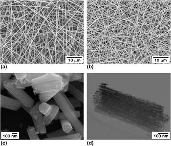
A spinning solution was electrospun to form 1D continuous TiO2/PVP composite nanowires with ∼400-nm diameter and quite smooth surface [Fig. 1(a)]. The thickness of electrospun mats could be easily controlled by adjusting the time for electrospinning. As shown in Fig. 1(b), after calcination, great shrinkage occurred, whereas the diameter of as-calcined nanowires was significantly smaller than the as-spun composite nanowires due to the decomposition of PVP and other organic contents; fortunately, the calcination did not affect the fibrous nature of the nanowires. After the heat treatment mentioned earlier, the average diameter of the nanowires was found to be restrained at ∼250 nm, which were very long over several centimeters. The TiO2 nanowires were mechanically broken to investigate morphological appearances at the cross-sectional surface and inside the wires. At high magnification of SEM and TEM images in Figs. 1(c) and 1(d), respectively, it was found that each calcined TiO2 wire was composed of a bundle of nanofibrils aligned in the wire direction.Reference Chuangchote, Jitputti, Sagawa and Yoshikawa13, Reference Chuangchote, Sagawa and Yoshikawa15
Scanning electron microscopy (SEM) images of (a) as-spun TiO2/polyvinylpyrrolidone (PVP) composite nanowires, (b) TiO2 nanowires calcined at 450 °C, and (c) mechanically broken TiO2 nanowires and transmission electron microscopy image of (d) broken TiO2 nanowires showing the morphology of aligned nanofibrils in the wire direction.

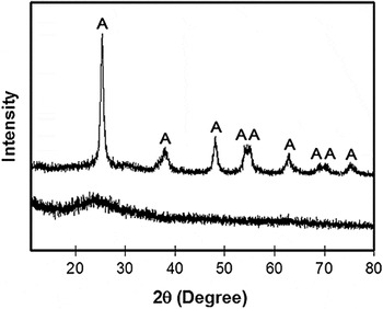
Figure 2 shows XRD patterns of as-spun TiO2/PVP composite nanowires and TiO2 nanowires calcined at 450 °C. As-spun TiO2/PVP composite nanowires showed two weak and broad peaks at 11° and 24° which refer to polycrystalline of PVP and amorphous TiO2 in composite nanowires. Calcination at 450 °C for 3 h resulted in high crystallinity. All diffraction peaks correspond well to a crystalline structure of the anatase TiO2.Reference Chuangchote, Sagawa and Yoshikawa15 These 1D characteristic, high crystalline, anatase TiO2 nanowires with aligned nanofibrils in the wire direction may promise to increase the efficiency of the hybrid photovoltaic cell in terms of preventing direct contact between the polymer and ITO substrate (which results in a decrease in efficiency as the result of recombination) and fast electron transportation. Therefore, hybrid photovoltaic cells made of electrospun TiO2 nanowires have been fabricated and investigated. It should be noted that electrospun TiO2 nanowires composed of pores between adjacent wires. Polymer may reach to ITO through the pores in nanowire matrix. To completely prevent the direct contact between the polymer and ITO substrate, a thin TiO2 hole blocking layer was also inserted between ITO and nanowire layers as mentioned in the “Experimental details.”
X-ray diffraction patterns of as-spun TiO2/PVP composite nanowires (lower) compared with TiO2 nanowires calcined at 450 °C (upper) (A = anatase TiO2).

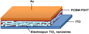
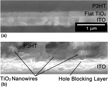
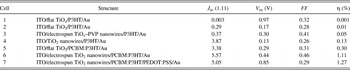
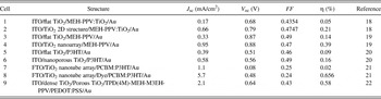
Figure 3 shows a cell structure of a TiO2 nanowire hybrid photovoltaic cell, while Table I summarizes the photovoltaic characteristics, including short-circuit current (J sc), open-circuit voltage (V oc), fill factor (FF), and power conversion efficiency (η) of devices made of TiO2 nanowires compared with other different organic–inorganic hybrid structures. Applications of TiO2 flat film or TiO2 nanowires as an electron acceptor material were initially studied (cells 1–4 in Table I). Conversion efficiencies of devices made of uncalcined TiO2 flat film and TiO2/PVP nanowires were very low (0.001 and 0.05%, respectively) because of low J sc, which attributed to low crystallinity of amorphous, uncalcined TiO2. On the contrary, upon calcination, increasing crystallinity resulted in increasing J sc and η (η of devices made of TiO2 flat film and TiO2 nanowires is 0.01 and 0.13%, respectively). Interestingly, J sc and η of nanowire devices were higher than those of flat film devices in both uncalcined and calcined TiO2 flat films. On the basis of the nanowire structure, aligned nanofibrils in nanowire direction with high surface area (56.3 m2·g−1)Reference Chuangchote, Jitputti, Sagawa and Yoshikawa13 are able to act as both electron acceptors and electron transporters to the ITO, which can be attributed to higher interfacial area for charge acceptance and charge separation from the donor material than that in flat film (diffusion length of the excitons in a semiconducting polymer is relatively shorter than 20 nmReference Savenije, Warman and Goossens16, Reference Arango, Johnson, Bliznyuk, Schlesinger, Carter and Horhold17). Figure 4 shows cross-sectional images of the devices made of TiO2 flat film and TiO2 nanowires. The images show that the devices made of TiO2 flat film consisted of flatly laminated P3HT film on the TiO2 film, whereas the devices made of TiO2 nanowires consisted of penetrated P3HT in TiO2 nanowire matrix. Good penetration of P3HT to nanowire matrix was due to the presence of pores between adjacent wires. This evidence also confirmed the higher interfacial area of the electron transporting and electron donor (polymer) materials in nanowire devices. Table II summarizes the cell performances of hybrid solar cells made of various forms of TiO2 from the opened literature. Kim et al.Reference Kim, Jo, Chun, Hong and Kim18 also reported that hybrid devices with higher surface contact of TiO2 and polymer resulted in higher J sc and η [see cells 1 and 2 in Table II, J sc and η of devices made of TiO2 two-dimensional (2D) structure > flat TiO2]. It is observed that electrospun TiO2 nanowires/P3HT devices exhibit comparable cell performances compared to flat TiO2, TiO2 2D structure, nanoporous TiO2, and TiO2 nanoarray (cells 1–6 in Table II).
Cell structure of hybrid devices made of electrospun TiO2 nanowires as an electron transporting material.

SEM images illustrating the penetration of polymer into inorganic layer in hybrid devices made of (a) flat TiO2 and (b) electrospun TiO2 nanowires.

Photovoltaic characteristics of devices made of different organic–inorganic hybrid structures.

J sc, short-circuit current; V oc, open-circuit voltage; FF, fill factor; η, power conversion efficiency; TiOx, uncalcined TiO2; P3HT, poly(3-hexylthiophene); PVP, polyvinylpyrrolidone; PCBM, 6,6-phenyl-C61-butyric acid methyl ester; PEDOT:PSS, poly(3,4-ethylenedioxythiophene):poly(styrenesulfonate).
Cell performances of hybrid solar cells made of various forms of TiO2 which were reported in the opened literature.

ITO, indium tin oxide; 2D, two-dimensional; MEH-PPV, poly(2methoxy-5-(2′-ethylhexyloxy)-1,4-shenylene-vinylene); FTO, fluorine-dopedSnO2 conducting glass; TPD(4M)-MEH-M3EH-PPV, poly{[1,4-phenylene-(4-methylphenyl)amino-4,4′-diphenylene-(4-methylphenyl)amino-1,4-phenylene-ethenylene-2-methoxy-5-(2-ethylhexyloxy)-1,-phenylene-ethenylene]-co-(2,5-dimethoxy-1,4-phenylene-ethenylene-2-methoxy-5-(2-ethylhexyloxy-1,4-phenylene-ethenylene)}.
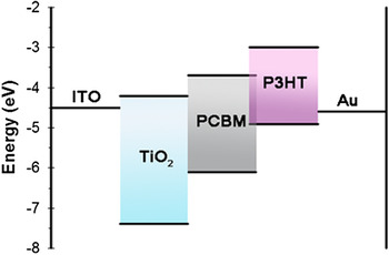
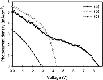
To improve the cell performance of TiO2 nanowires/P3HT hybrid devices, we mixed PCBM to the system. In this sense, PCBM acts as an electron acceptor, whereas TiO2 nanowires act as an electron transporter only because charge separation occurs at the interface of PCBM/P3HT more likely than that of TiO2 nanowires/P3HT (which can be seen in the energy diagram in Fig. 5). With PCBM, η of devices was improved as a result of increasing J sc. Again, devices made of TiO2 nanowires exhibited remarkable improvement of the cell efficiencies in terms of J sc and V oc as compared with those of references, TiO2 flat films, as shown in Fig. 6 (η of nanowire and TiO2 flat devices is 1.11 and 0.30, respectively). This η of nanowire devices was higher than a similar hybrid system made of TiO2 nanotube array (see cells 7 and 8 in Table II), even though nanowires were not modified with any dye.
Schematic energy level diagram of device investigated in this work.

Photocurrent density–voltage (J–V) characteristics of hybrid devices with different structures: (a) ITO/flat TiO2/PCBM:P3HT/Au, (b) ITO/electrospun TiO2 nanowires/PCBM:P3HT/Au, and (c) ITO/electrospun TiO2 nanowires/PCBM:P3HT/PEDOT:PSS/Au. ITO, indium tin oxide; PCBM, 6,6-phenyl-C61-butyric acid methyl ester; P3HT, poly(3-hexylthiophene).

Ravirajan et al.Reference Ravirajan, Bradley, Nelson, Haque, Durrant, Smit and Kroon22 (see cell 9 in Table II) reported an efficient charge collection in hybrid TiO2/polymer cells by introducing a poly(3,4-ethylenedioxythiophene):poly(styrenesulfonate) (PEDOT:PSS) layer under the gold electrode as a hole collector. We also applied PEDOT:PSS to our devices to improve the overall efficiency (cell 7 in Table I). PEDOT:PSS (Baytron P, H.C. Starck, Leverkusen, Germany) in aqueous dispersion was spin coated on top of the PCBM/P3HT layer, followed by annealing at 110 °C for 4 min before depositing the Au electrode. Lines (b) and (c) in Fig. 6 show J–V characteristics of devices without and with PEDOT:PSS, respectively. The PEDOT:PSS layer significantly increased the V oc from 0.44 to 0.85 V. The J sc and FF, however, slightly decreased (J sc from 5.57 to 5.05 mA/cm2 and FF from 0.46 to 0.29). The increase in V oc was expected because it was controlled by the difference in electrode work functions (the difference between the work functions of ITO and Au is larger by insertion of PEDOT:PSS layer underneath Au). Note that increasing V oc after the insertion of PEDOT:PSS was also expected in Ref. Reference Ravirajan, Bradley, Nelson, Haque, Durrant, Smit and Kroon22. For the decreases of J sc and FF, one explanation is that the PEDOT:PSS solution had very low contact and wettability on the polymer layer because it was dispersed in aqueous solution. PEDOT:PSS could not cover smoothly on the devices. Another possibility is that aqueous solution of PEDOT:PSS may damage the polymer film during spin coating, which could lead to an increase in the series resistance of the device (i.e., series resistances of cells 6 and 7 in Table I are 0.46 and 1.26 MΩ, respectively). Comparing the results again with Ref. Reference Ravirajan, Bradley, Nelson, Haque, Durrant, Smit and Kroon22, the same PEDOT:PSS was used in both studies, but J sc in Ref. Reference Ravirajan, Bradley, Nelson, Haque, Durrant, Smit and Kroon22 was found to increase with insertion of PEDOT:PSS, whereas it was found to slightly decrease in this work as a result of low contact and wettability of PEDOT:PSS on the polymer layer as described earlier. Different polymers used may be one of the reason, P3HT and poly(p-phenylene vinylene)-based polymer in this work and in Ref. Reference Ravirajan, Bradley, Nelson, Haque, Durrant, Smit and Kroon22, respectively. In the recent progresses of TiO2/PCBM:P3HT devices, good wettability of PEDOT:PSS on polymer layer could achieve η of devices up to 2–3%.Reference Kuwabara, Sugiyama, Yamaguchi and Takahashi23, Reference Yodyingyong, Zhou, Zhang, Triampo, Xi, Park, Limketkai and Cao24 Therefore, for further study, improvement of wettability and compatibility (with polymer) of PEDOT:PSS disperse is very necessary. Anyway, in this step, PEDOT:PSS layer relatively increase η of nanowire hybrid devices from 1.11 to 1.27%.
IV. CONCLUSIONS
Hybrid organic–inorganic photovoltaic cells made of TiO2 nanowires were fabricated. TiO2 nanowires were directly electrospun onto ITO on glass substrate from a solution in methanol of PVP, TiBu, and ACA. The nanowire electrode obtained was consequently subjected to calcination at 450 °C. Calcined TiO2 nanowires were 250 nm in diameter, several centimeters in length, and contain pure anatase crystalline phase. Solution of P3HT and PCBM was spin coated on the TiO2 electrode, followed by thermal annealing and deposition of Au electrode. Hybrid organic–inorganic photovoltaic cells made of TiO2 nanowires exhibited remarkable improvement of the cell efficiencies in terms of photocurrent density and open-circuit voltage as compared with those of references, TiO2 flat films. Maximum energy conversion efficiency of hybrid organic–inorganic photovoltaic cells made of TiO2 nanowires of 1.27% could be achieved with inserting a hole-collecting layer.
ACKNOWLEDGMENT
This work was supported in part by a Grant-in-Aid from the Japan Society for the Promotion of Science (JSPS) under the JSPS Postdoctoral Fellowship for Foreign Researchers.