Introduction
Over the past few years, increasing demand for clean energy has resulted in several innovations, particularly in the field of photovoltaics. Research in solar cells ranging from exploration of new materials and morphologies to integration of photonic elements to improve light trapping has been constantly growing. Most photovoltaic studies can be broadly categorized into four areas: photon harvesting, photon absorption, photon-to-electron conversion, and extraction of photo-generated electrons. To maximize the amount of sunlight incident on a solar cell and improve photon harvesting, advances have been made in the development and implementation of concentrators[ Reference Xing, Han, Wang, Liang, Lou, Zhang, Hu, Zhu, Zhao and Mi 1 ] and trackers.[ Reference Mousazadeh, Keyhani, Javadi, Mobli, Abrinia and Sharifi 2 ] Incorporating anti-reflective coatings[ Reference Raut, Ganesh, Nair and Ramakrishna 3 ] as well as complex ordered, aperiodic, or random optical structures has led to improved absorption of photons incident on a solar cell.[ Reference Bozzola, Liscidini and Andreani 4 – Reference Trevino, Forestiere, Di Martino, Yerci, Priolo and Dal Negro 7 ] More efficient photon-to-electron conversion in solar cells has been made possible by band gap engineering, including multi-junction cells in III–V[ Reference Jani, Ferguson, Honsberg and Kurtz 8 ] and II–VI[ Reference Gloeckler and Sites 9 ] materials. To achieve more efficient extraction of photo-generated electrons from a solar cell into an external circuit, various materials including transparent conducting oxides have been studied and utilized as electrical contacts.[ Reference Stadler 10 , Reference Granqvist 11 ] Despite these advances and a progressive increase in efficiency, with a recent III–V module reaching 43.4% efficiency,[ Reference Green, Emery, Hishikawa, Warta and Dunlop 12 ] solar cells account only for 1% of global electricity production.[ 13 ] Wide-scale adoption of many of the aforementioned advances into large-scale manufacturing has not occurred due to the expense of the materials or processing techniques. Hence, there remains a critical need to find cost-effective solutions to improve solar cell performance.
This work suggests two such methods for achieving improved light trapping, along with increased solar cell efficiency, in amorphous silicon solar cells with little impact on the processing cost of the cell. We focus on amorphous silicon solar cells, as this class of solar cells is known to have relatively low production costs in comparison with crystalline silicon solar cells and can be fabricated on either flexible or rigid substrates. Several back reflector designs have been combined with amorphous silicon-based solar cells to enhance light trapping, including random textured transparent conducting oxides,[ Reference Müller, Rech, Springer and Vanecek 14 ] patterned photonic crystal structures,[ Reference Curtin, Biswas and Dalal 15 ] and plasmonic nanostructures.[ Reference Atwater and Polman 16 ] Here, we demonstrate simple and cost-effective back reflectors that scatter unabsorbed light back into the active region of an amorphous silicon cell, leading to enhanced photon absorption. In one approach, we use metal-assisted chemical (MAC) etching to porosify and roughen a layer of hydrogenated amorphous silicon (a-Si:H). In a second approach, we imprint a grating pattern into a porous a-Si:H layer using the simple direct imprinting of porous substrates (DIPS) technique,[ Reference Ryckman, Liscidini, Sipe and Weiss 17 ] which could be implemented in roll-to-roll manufacturing. Our fabrication approaches are versatile and can be applied to various rigid or flexible substrates (e.g., polymer or glass), similar to those on which amorphous silicon-based cells are currently being fabricated.
Grating back reflector design
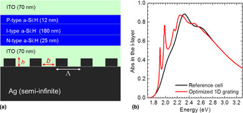
A sketch of the structure used for the design of the grating back reflector is shown in Fig. 1(a). It consists of a n–i–p stack of a-Si:H sandwiched between two layers of indium tin oxide (ITO), with a periodically patterned silver back reflector. The simulation considered a semi-infinite silver substrate; it was assumed that all the light incidents on the metal layer was reflected from or absorbed by the metal. The grating depth is denoted with h, the lattice period with Λ, and the ITO fraction with b/Λ. The grating back reflector design was determined based on rigorous coupled wave analysis (RCWA) simulations[ Reference Bozzola, Liscidini and Andreani 4 , Reference Liscidini, Gerace, Andreani and Sipe 18 , Reference Andreani, Bozzola, Kowalczewski and Liscidini 19 ] that made use of experimentally determined optical constants of the individual layers, which have been obtained using spectroscopic ellipsometry. A comparison of the simulated and experimentally measured reflectance of a flat n–i–p a-Si:H cell with front and back ITO contacts shows good agreement for energies <2.4 eV and confirms the validity of the theoretical approach used to describe the optical properties of the system (see Supplementary Material).
(a) Cell structure for the RCWA simulations. (b) Simulated absorption enhancement in a-Si:H cell with 1D silver grating with height of 60 nm, 500 nm period, and fill fraction of 60%.

In the design of the periodic patterned substrate, we considered a one-dimensional (1D) grating to reduce computation time; we also assumed that the n–i–p layers and contact layers were flat. From previous studies,[ Reference Bozzola, Liscidini and Andreani 4 ] we know that optimized 1D and 2D gratings for light trapping are characterized by similar values of the parameters h, Λ, and b. Our calculations lead to a conservative estimate in the absorption, for they do not account for any light that is scattered due to roughness contributed by the underlying porous a-Si:H layer and the grating structure transferred to the n–i–p layers. Finally, it is well known that 2D gratings can lead to larger absorption enhancement than 1D gratings due to the opening of more scattering channels.[ Reference Bozzola, Liscidini and Andreani 4 ]
The absorption in the intrinsic layer of the cell with the grating back reflector was maximized by varying the parameters h, Λ, and b/Λ. The numerical strategy adopted in this work allows one to calculate the absorption solely in the intrinsic layer, which gives the relevant contribution to the photocurrent, while also taking into account losses in the p- and n-doped layers, which are described by their complex dielectric functions derived by ellipsometric measurements.[ Reference Zanotto, Liscidini and Andreani 20 ] The RCWA calculations suggested that a 1D grating with a period of 500 nm, height of 60 nm, and fill fraction of 60% should provide a 16% increase in the short-circuit current with respect to a cell with a flat metal back reflector. The estimated absorption enhancement is shown in Fig. 1(b). The absorption peaks between 1.8 and 2 eV are due to the coupling of light in the guided modes supported by the high-index silicon layers in the cell stack.
Porous a-Si:H back reflector fabrication
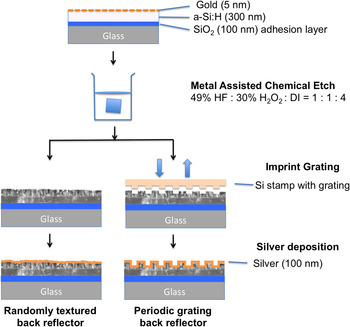
The a-Si:H solar cell was fabricated on a glass substrate (Corning EAGLE XG), which was first rinsed with isopropyl alcohol, ethanol, and methanol to remove any contaminants adhering to the surface. A 100 nm SiO2 layer was deposited on the glass substrate using plasma-enhanced chemical vapor deposition (PECVD) to promote the adhesion of the a-Si:H layer used to form the back reflector. Figure 2 shows a schematic illustrating the two approaches for back reflector fabrication. It was found that samples prepared without the thin SiO2 layer delaminated during the a-Si:H porosification process. The a-Si:H layer used for the back reflector formation was a lightly p-doped 280 nm thick a-Si:H layer deposited via PECVD with 10% silane (SiH4) diluted with He, 2% trimethylboron [TMB, B(CH3)3] diluted with hydrogen (H2), and H2. The band gap of the a-Si:H film was estimated to be 2 eV based on using the Tauc method to fit spectroscopic ellipsometry data.
Schematic illustrating the fabrication of the two back reflector designs implemented in porous a-Si:H.

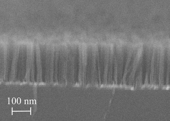
To porosify the a-Si:H layer to achieve a roughened surface that promotes light trapping, MAC etching was carried out. Extensive work has been done to characterize MAC etching of silicon and other semiconductor materials, including several studies on MAC-etched silicon nanowires for enhanced light trapping and carrier extraction in solar cells.[ Reference Huang, Geyer, Werner, de Boor and Gösele 21 – Reference Li 23 ] However, very few studies have been conducted on MAC etching of amorphous silicon.[ Reference Omampuliyur, Bhuiyan, Han, Jing, Li, Fitzgerald, Thompson and Choi 24 – Reference Douani, Piret, Hadjersi, Chazalviel and Solomon 26 ] In one of these studies, Douani et al. carefully investigated the formation of hydrogenated amorphous silicon–carbon alloy nanowires using a hydroflouric acid (HF)/AgNO3 solution and reported the dependence of the nanowire morphology on substrate doping, etchant concentration, and etching time.[ Reference Douani, Piret, Hadjersi, Chazalviel and Solomon 26 ] In our work, MAC etching of a-Si:H was carried out with a discontinuous 5 nm layer of thermally evaporated gold acting as the catalyst. Three parameters of the MAC etch were explored in detail, as explained in Supplementary Material: the molar concentrations of [HF] and hydrogen peroxide [H2O2] in the etchant, the time delay between carrying out the a-Si:H deposition and the MAC etch, and the MAC etch duration. As the ratio of [HF]:[H2O2] was decreased, the morphology of the MAC etched a-Si:H layer changed from a dense, spike-like structure to grass-like to sparse short stumps. The grass-like morphology was identified to be most favorable as a textured surface to encourage light trapping and, consequently, a MAC etch composition of 49% HF, 30% H2O2, and deionized (DI) water in the ratio of 1:1:4 was selected. We found that if the MAC etch was performed immediately after the a-Si:H and gold depositions, it did not result in a very porous surface. On the contrary, if the etch was performed after 24 to 48 h, the desired textured, porous substrate was obtained. We hypothesize that this difference in behavior is due to the hygroscopic nature of a-Si:H, which absorbs moisture upon exposure to air, thus impacting the nature of the MAC etch. Finally, we investigated the MAC etch duration. An etch time of 45 s resulted in a 150 nm porous layer, as shown in Fig. 3. Longer etch times did not increase the thickness of the porous layer significantly, and instead the etch began to progress along weak pathways in the a-Si:H and undercut at the a-Si:H and SiO2 interface. To complete the formation of the textured back reflector, the porous a-Si:H layer was coated with a 5 nm thick chromium adhesion layer followed by a 100 nm thick layer of silver.
Cross-sectional SEM image of porous a-Si:H obtained from a 45 s MAC etch.

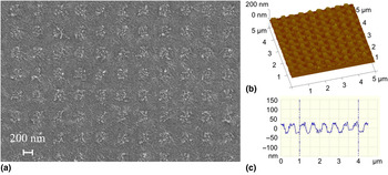
To form a cost-effective patterned back reflector, we further processed a MAC-etched porous a-Si:H layer by imprinting it with a 2D grating pattern—with the dimensions suggested by the RCWA simulations (Λ = 500 nm, b/Λ = 60%, and h = 50–60 nm)—using DIPS. The 2D grating was symmetric and employed the same grating pitch and fill factor (FF) in both dimensions. The 2D grating was selected for fabrication due to its predicted improved light scattering ability compared with a 1D grating. DIPS was performed by pressing a grating patterned silicon stamp into a porous a-Si:H layer using a hydraulic press.[ Reference Ryckman, Liscidini, Sipe and Weiss 17 ] A pressure of 170–180 psi was applied to a 4.5 × 4.5 mm2 stamp. Prior to performing the imprintation, the surface of the silicon stamp was oxidized at 800 °C for 30 min and silanized overnight in an evacuated desiccator containing an open glass vial with 70 µl of Triphenylcyclopropenylium Hexafluoroantimonate (TCPF) in order to minimize adhesion of the porous a-Si:H to the stamp.[ Reference Mares, Fain, Beavers, Duvall and Weiss 27 ] Representative scanning electron microscopy (SEM) and atomic force microscopy (AFM; Digital instruments Nanoscope III) images of a 2D DIPS grating in porous a-Si:H are shown in Fig. 4. The AFM scan shows an RMS roughness of 13 nm. After the imprinting, the porous a-Si:H grating was coated with a 5 nm thick chromium adhesion layer followed by a 100 nm thick layer of silver, completing the metallic grating back reflector.
Images of a 2D grating imprinted on porous a-Si:H using DIPS are shown: (a) top view SEM image, (b) AFM image, and (c) AFM line scan.

Fabrication of n–i–p layers of a-Si:H solar cell and ITO contacts
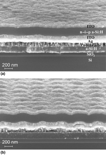
The remainder of the a-Si:H cells was fabricated on top of the back reflectors beginning with the back contact. A 60 nm thick ITO layer was sputtered using an Angstrom Åmod RF magnetron sputter tool. The layer was deposited at 200 °C using an argon plasma with 1% O2. This method of deposition resulted in a layer with a resistivity of 6.7 × 10⁻⁴ Ω-cm, as measured by a hand held four-point probe meter (SRM-232-1000). The sample was then transferred to the PECVD chamber for n–i–p a-Si:H depositions; during these depositions, a small area in the corner of the sample was covered with a piece of silicon that acted as a mask and allowed access to the bottom ITO contact for measurements on the completed solar cell. The n, i, and p-layers were deposited sequentially at 200 °C and 600 mT for all layers. The n-layer was doped with phosphorous using 1% phosphine (PH3) diluted in He as the dopant gas, while the p-layer was formed using TMB during the deposition. Detailed recipes for the n–i–p layers are included in Supplementary Material. A clean was performed in between the n- and i-layer depositions to prevent PH3 from contaminating the intrinsic region of the device. The thicknesses of the p, i, and n-layers were 12, 180, and 25 nm, respectively. The cells were completed by sputter depositing a 60 nm thick ITO layer as the top contact. The same recipe as detailed previously for the bottom ITO contact was followed at a lower temperature of 175 °C in order to reduce the impact of high-temperature processing on the underlying a-Si:H device layers, resulting in a resistivity of 7.5 × 10⁻⁴ Ω-cm. A stainless steel contact mask was used during the deposition to pattern the ITO with 0.07 cm2 circular cells. Figure 5 shows SEM images of completed a-Si:H solar cells with the textured, MAC-etched porous a-Si:H back reflector and the imprinted porous a-Si:H grating back reflector. The random roughness introduced by the MAC etch is clearly shown and is distinct from the more regular grating pattern.
Cross-sectional SEM images of a-Si:H solar cells with (a) textured porous a-Si:H back reflector and (b) 500 nm pitch, 60% fill fraction porous a-Si:H grating back reflector For imaging purposes, these cells were fabricated on a silicon substrate instead of glass, but were processed at the same time as the cells on glass substrates that were electrically characterized.

Electrical characterization of solar cell performance
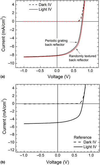
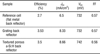
A LabView controlled Keithley 2400 source meter was used to perform the light and dark I–V measurements to characterize the solar cell performance. The light source was a 100 W Xenon ozone-free lamp with an AM1.5G filter. Prior to the measurement, the intensity of the light source was calibrated to maintain one sun conditions, which is equivalent to an irradiance of 100 mW/cm2, by using a standard c-Si reference cell with an integrated KG5 window. Performance of the a-Si:H solar cells with the textured porous a-Si:H back reflector and imprinted a-Si:H grating back reflector was compared with a reference cell fabricated on a flat silver back reflector without the porous a-Si:H layer. As shown in Fig. 6 and Table I, an approximately 30% enhancement in both short-circuit current (J sc) and overall efficiency was observed in the a-Si:H cells with the porous a-Si:H back reflectors. The textured porous a-Si:H back reflector and the imprinted grating back reflector both led to a similar performance enhancement. The reported enhancements are average values measured across the four best cells on each sample. As discussed earlier, the measured enhancement is greater than that predicted by 1D simulations that did not account for absorption arising from the rough texture of the porous a-Si:H and the transferring of the grating pattern to all the layers of the cell. It should be noted that, as expected, both the texturing and grating approaches lead to improved optical performance as quantified by the increase in J sc, while the electrical performance quantified by the open-circuit voltage (V oc) and FF remain largely unchanged.
I–V characteristics obtained from a-Si:H n–i–p solar cells with (a) metal-coated porous a-Si:H back reflector with (black) and without (red) imprinted grating and (b) flat metal back reflector. A 30% increase in J sc is observed due to the addition of the porous a-Si:H layer with either the randomly textured or periodic grating back reflector.

I–V measurement results.

It is not entirely surprising that the cells with the textured porous a-Si:H back reflector and grating back reflector showed little difference in their I–V characteristics, for it is known that the use of rough substrates can lead to absorption enhancements that are comparable with those determined by perfectly periodic structures.[ Reference Kowalczewski, Liscidini and Andreani 28 ] Prior studies have extensively investigated the effect of grating design on the light-trapping properties of amorphous silicon thin-film solar cells as well as the tradeoff between optimizing the optical and electrical properties of amorphous silicon solar cells through the use of random versus periodic nanostructures.[ Reference Bozzola, Liscidini and Andreani 4 , Reference Battaglia, Hsu, Söederströem, Escarré, Haug, Charrière, Boccard, Despeisse, Alexander, Cantoni, Cui and Ballif 29 ] Our work is significant in its experimental demonstration of comparable absorption enhancements from random texturing and periodic gratings on the same amorphous silicon platform. Further enhancement of amorphous silicon solar cell performance may be achieved by following two different routes. In a first approach, the MAC etch conditions could be further refined to achieve a morphology with a more isotropic absorption enhancement approaching the Lambertian limit to light trapping.[ Reference Green 30 ] A second strategy may be the optimization of the 2D grating parameters including micro-roughness on a sub-wavelength scale or introducing a controlled degree of disorder. In both routes, electrical transport issues will need to be considered being mindful of the aforementioned trade-off between optical and electrical properties and the impact on overall cell efficiency.
Conclusions
This work demonstrates the cost-effective integration of porous a-Si:H-based grating back reflectors with a-Si:H n–i–p solar cells. In the first approach, MAC etching was used to form a randomly textured porous a-Si:H layer that was covered with a thin layer of silver to obtain a rough back reflector. In the second approach, a porous a-Si:H layer was imprinted with a periodic grating pattern and then coated with a thin layer of silver to transfer the periodic pattern to the silver back reflector. The grating was optimized via RCWA calculations, which provided a conservative estimate of a 16% increase in short circuit current for a 1D grating design with a grating period of 500 nm, grating height of 60 nm, and grating fill fraction of 60%. The fabricated cells, with either the textured porous a-Si:H back reflector or the 2D periodic pattern, showed an approximately 30% increase in short-circuit current and overall cell efficiency compared with a reference cell with a flat metal back reflector. It should be noticed that, although the measured photocurrent enhancements are similar, they originate by different mechanisms, which depend on the different length scales over which the refractive index is modulated. In the first case, the optical performance enhancement of the cell was primarily attributed to back scattering of light due to the randomly textured surface of the porous a-Si:H layer, which was believed to lead to a relatively isotropic absorption enhancement. In the second case, the optical performance enhancement was primarily attributed to diffraction and coupling of incident radiation into quasi-guided optical modes, which are expected to lead to strong wavelength-dependent absorption enhancement. Further improvements may be achieved through refined grating design and fabrication, optimization of the roughness of the porous amorphous silicon layer, or a combination of those approaches. This work suggests that the addition of a porous amorphous silicon-based back reflector using inexpensive processing techniques can lead to improved amorphous silicon solar cell performance over large areas in a cost-effective manner.
Supplementary Material
The supplementary material for this article can be found at http://dx.doi.org/10.1557/mrc.2016.15.
Acknowledgments
This work was supported in part by the Defense Threat Reduction Agency (DTRA) grant no. HDTRA1-10-1-004 and the National Science Foundation through the Tennessee Solar Conversion and Storage Outreach, Research and Education (TN-SCORE) grant no. NSF EPS-1004083. Fabrication of the silicon grating stamps was conducted at the Center for Nanophase Materials Sciences, which is a DOE Office of Science User Facility. Solar cell fabrication was carried out in the Vanderbilt Institute of Science and Engineering (VINSE). The authors thank C. D. Hungerford, G. A. Rodriguez, J. W. Mares, and K. J. Miller for their technical assistance.