I. INTRODUCTION
In the last decades, radar systems found their way into numerous industrial applications. Therefore, one common application is the tank level probing radar (TLPRs). It is used to determine the filling level of silos or tanks. Therefore, basic requirements for efficient TLPR-systems are the resolution, the accuracy, and the cost. While the resolution deteriorates due to dispersion, signal attenuation decreases the signal-to-noise ratio which influences the accuracy of the radar negatively. By now, we observe two trends concerning industrial radar systems. Firstly, operating frequencies increase due to the simultaneously increasing operation bandwidth, which results in higher range resolutions. A prominent TLPR system with a center frequency at 80 GHz was introduced in [Reference Jaeschke, Vogt, Baer, Bredendiek and Pohl1]. Secondly, the contact free measuring method of TLPRs is ideally suited for the operation in harsh industrial environments like high temperature environments or potentially explosive atmospheres. For the explosive atmosphere operation, TLPR systems have to comply various safety requirements like the DIN-EN-50020. Furthermore, in case of high temperature applications, cooling zones must be kept to ensure proper functionality of the radar system. Therefore, the transition between electronic and antenna must be extended, which leads to increased dispersive behavior at higher frequencies.
Although, these requirements are necessary due to safety reasons, they prevent the utilization of commonly used transitions or feedings. Hence, high frequency radar systems are often not applicable for high temperature applications or in potentially explosive atmospheres. In this contribution, we present dielectric waveguides (DWGs) that were designed and manufactured to fulfill a non-dispersive behavior as well as to meet the mentioned requirements. The presented DWGs were designed for operating frequency range from 75 to 90 GHz.
Based on the results from [Reference Baer, Schulz, Rolfes and Musch2], we have structured this article as follows. In chapter two, we illustrate three challenging industrial environments that limit the applicability for common TLPR systems. In chapter three, we discuss fundamentals concerning DWG and explain basic design rules. Further, we introduce three different DWG setups that are suitable for the mentioned environments and we present first measurement results in chapters four–six. Finally, we give a short conclusion in chapter seven.
II. CHALLENGING INDUSTRIAL APPLICATION
A) Explosive environment
All electronic measuring devices that are used in explosive environments, as shown in Fig. 1(a), are subject of special regulations. Therefore, the DIN-EN-50020 regulates the minimum creep distance between electrical conductors and frame ground to prevent spark overs. Standard TLPR systems often use circular waveguides (CWGs) for connecting the radar device with the antenna because of their simple and cost effective manageability. However, microstrips to waveguide transitions as shown in [Reference Enayati, Brebels, Vandenbosch and De Raedt3] are shrinking for higher frequencies. Accordingly, the distance between rf-signal line and CWG-metalization, which has frame ground potential, scales below the minimum creep distance, makes the whole system inapplicable. Hence, we have to ensure that all metal components, which are accessible, have to be on frame ground. This is also compulsory for CWGs or TLPR antennas. Furthermore, for preventing sparkovers, we have to guarantee that creep distances in air, pottant, or isolation material must be greater than 49, 5.3, and 2.7 mm, respectively. Therefore, we are facing difficulties for radar devices above 30 GHz when a CWG connects the printed circuited board (PCB) with the antenna, because common PCB–CWG transitions provide only smaller distances [Reference Schulz, Pohl and Rolfes4].
Schematical drawings of different scenarios: (a) explosive environment, (b) side mount application, and (c) high-temperature environment.

B) Limited installation space
Another challenging scenario arises, when the installation space on the tank's roof is limited. This can occur when additional installations like filters, filler plugs, or other measuring devices extend into the tank's interior. Furthermore, some tanks are located inside of a surrounding building, which does not allow for tank roof access. In all these cases, we are facing problems with the common roof installation of the TLPR. Therefore, a possible solution is a wall-mounted TLPR. Fig. 1(b) shows a schematical drawing of the outlined scenario. However, to perform the radar measurement in the familiar manner, we need a bended transition from the electronic part to the antenna. Yet, common approaches for bended waveguides can be found in [Reference Nantista, Kroll and Nelson5, Reference Li, Cao and Yao6]. However, CWG-bends often excite higher order modes that increase dispersion, which influences the TLPR accuracy negatively.
C) High-temperature environment
In the context of chemical and process industry sites, batch processing is an economically advantageous method because it saves resources and expensive materials. Therefore, different chemical products are filled in and blended inside of a so-called batch-container on demand. In many cases, mixtures must be heated up to perform the molding process adequately. Fig. 1(c) shows a schematical drawing of a batch container. Since the product temperature can reach several hundred degree celsius, TLPR systems may not be mounted directly to the container's roof. Other high temperature environments can be found in the coal and steel industry. Therefore, cooling installations, heat protection, or so-called heat-resistant transitions must be used to ensure high temperature stability for the TLPR and may not influence its accuracy.
III. FUNDAMENTALS
We know DWGs in rf-engineering for around a hundred years by now. In [Reference Hondros and Debye7], Hondros and Debye set up a first mathematical model for transverse magnetic mode propagation in dielectric materials. Furthermore, Chandler [Reference Chandler8] and Carson et al. [Reference Carson, Mead and Schelkunoff9], discussed a general theory for the existence of TE, TM, and hybrid HE modes. Because the theory of DWGs is known for years and well described in [Reference Carson, Mead and Schelkunoff9, Reference Adler10], we will only recap a few basic remarks concerning the propagation modes.
In terms of CWGs, we know the cut-off frequency, which limits the wave propagation for frequencies below the cut-off frequency. Furthermore, we are aware that the CWG's cut-off behavior causes dispersion. However, the dispersive influence caused by the cut-off frequeny does not apply to DWGs even though we can also determine a characteristic frequency. Below the so-called divergence frequency, the DWG structure does not guide electromagnetic waves anymore and we can observe free space propagation [Reference Adler10, Reference Gyorgy and Weiss11].
Nevertheless, this means that the DWG provides low dispersion while guiding the electromagnetic wave. However, it is evident that a certain number of propagation modes for DWGs exist. Most of these modes have longitudinal components of both, E and H field. We call these modes hybrid modes and symbolize them by HE nm . To build up an adequate DWG, we have to comply with several requirements:
-
(1) The chosen mode should be excited easily.
-
(2) The transmission behavior should be as loss-free as possible.
-
(3) Manufacturing tolerances may not cause conversion or radiation effects.
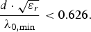
Apparently, the HE11-mode seems to be a good choice, because its field pattern is very similar to the TE11-mode, which is the fundamental mode of a CWG. Figures 2(a) and 2(b) show the field patterns of the TE11-mode and the HE11-mode, respectively. We can excite the HE11-mode very simple by inserting a dielectric fiber into a CWG. To ensure a proper transition, we may step the dielectric fiber's diameter on the CWG's side. When a stepped impedance match is not possible, e.g. due to fabrication, we also may chose a cone-shaped match. Furthermore, a tapered CWG design on the fiber's side will effect the transition behavior positively. Concerning the loss, we can show that the HE11-mode minimizes loss over wide diameter ranges compared with other modes [Reference Gyorgy and Weiss11]. Furthermore, we can assume that the diameter has great influence on mode-conversion. However, if we keep the diameter to wavelength ratio small, it will guarantee a mode-conversion free operation. As a critical value, we can assume:
 $$\displaystyle{{d \cdot \sqrt {\varepsilon _r } } \over {\lambda _{0\comma \min } }}\lt 0.626.$$
Here, d is the diameter of the DWG, ε r the relative permittivity, and λ 0, min the free space wavelength of the highest operating frequency. In terms of radiation behavior, we can assume that fiber discontinuities will always cause radiation. However, since all modes provide this radiation behavior, the HE11-mode is a good choice.
E-Field pattern of: (a) TE11-mode and (b) HE11-mode.

IV CREEP DISTANCE AND INSULATION SETUP
As already mentioned, electrical insulation of mmWave components is an issue when TLPRs are used in an explosive environment. Nevertheless, we can solve the mentioned feeding problems by means of a DWG. Figure 3 shows the necessary parts of the proposed assembly. Due to radiation reasons, we have to seal the whole structure with a concentric metallic housing, which is illustrated in Fig. 3(a). The housing is, except for the diameter of a metallic CWG, closed on the antenna side. On the radar device side, the housing is opened and can be connected to the device housing. To fulfill the creep distance regulations, we have to choose the inner diameter of the housing to be large enough, which can be realized in most cases without problems. The next concentric layer of the setup contains the insulation material. It is shown in Fig. 3(b). The evanescent fields of the dielectric fiber excite higher order modes inside the metallic frame. These modes propagate along the cylindrical housing, reflect at the end of the housing multitudinously, and interfere with the fiber-guided signal. Therefore, we prefer lossy dielectric materials as insulator to attenuate higher order modes. Finally, we position a spacer material as well as the dielectric fiber in the center of the insulation layer. They are illustrated in Figs. 3(c) and 3(d). The spacer material is required to reduce the insulator's influence on the DWG. Therefore, the spacer material possesses a very low permittivity. As long as the mode requirement (1) is kept, nearly all dielectric materials are suitable. On the antenna side of the DWG as well as on the radar device side, the fiber is connected to a DWG feeding as illustrated in Fig. 3(e). While the feeding is set on frame ground on the antenna side, it can be set on any electrical potential on radar device side as shown in Fig. 3(f). As long as the insulation layer is large enough, all requirements concerning creep distances are met.
Schematical drawing of the dielectric guide showing: (a) metallic housing, (b) insulation layer, (c) spacer, (d) DWG, (e) feedings, and (f) complete setup.

A) Simulations
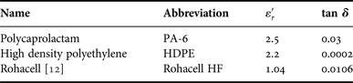
Three-dimensional (3D) electromagnetic field simulations are an indispensable tool for the development and optimization of rf-components. Within CST Microwave Studio 2013 we performed various, broadband simulations. The modeled structure of the DWG is 25 cm long and provides a diameter of 4 cm. To ensure accurate simulation results, a hexahedral mesh type was used. Its definition is given by the “lines per wavelength” and the “lower mesh limit”, which were set to 10 and 5, respectively. A “mesh line ratio limit” of 10 was used which yields a total mesh of approximately 32 million mesh cells. Furthermore, the time domain solver with a simulation accuracy of −60 dB was utilized. Regarding the excitation, the CWG part of the transitions were stimulated with the TE11-mode for a frequency range from 75 to 90 GHz. Firstly, we optimized the transistion CWG–DWG to guarantee a proper excitation of the desired HE11-mode. In further simulations, the fiber diameter steps and the transition tapers were optimized in terms of improved return loss. Therefore, the optimum simulation results were achieved by using two impedance steps with diameters of 1.4 and 0.5 mm and a cylindrical step-length of 1.4 mm each. Finally, we modeled and optimized the surrounding of the fiber, which contains the spacer layer, the insulation layer, and the metallic housing. As a convenient material for the lossy insulation layer, which is widely spread, we chosed polycaprolactam (PA-6). It is used because of its attenuative behavior and easy processability.
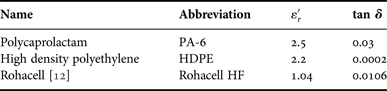
Furthermore, it is cost efficient which makes it suitable for industrial applications. The dielectric properties of PA-6 that were used for the simulation are shown in Table 1. Within the simulation, the other materials parameter were optimized in a realistic range of values to find adequate materials later on. Figure 4(a) shows the return and insertion loss of the whole structure. With a return loss of at least 15 dB for the whole frequency range the waveguide–fiber transitions meet the requirements. Furthermore, the insertion loss is better than 0.35 dB, which shows the nearly loss-free behavior of the DWG. By means of the time domain signals, the dispersive behavior was investigated. Therefore, the transition was shortened on the antenna side. Figure 4(b) shows the envelopes of the normalized excitation pulse |s exc (t)| as well as the received pulse |s rec (t)|. With a relative pulse-spreading of the 3 dB pulsewidth of 10%, the DWG can be assumed nearly dispersion free.
Results of the simulation showing (a) the return and insertion loss, (b) the normalized excitation pulse, and the received pulse.

Dielectric properties of utilized materials for the insulation setup.
B) Measurements
To prove the presented properties of the DWG, the whole structure was built up.
Figures 5(a) and 5(b) show photographs of the disassembled components and the mounted DWG, respectively. The outer diameter of the metallic housing, as shown in Fig. 5(a)(1), is 5 cm. The insulation material, shown in Fig. 5(a)(2), is PA-6 as already used in the simulations. By means of the simulation based optimization the other materials were chosen to be as follows. The spacer element, illustrated in Fig. 5(a)(3), is made of Rohacell HF. It possesses a very low permittivity compared with the fiber and is nearly loss-free. The fiber, illustrated in Fig. 5(a)(4), is made of high-density polyethylene (HDPE), which was chosen because of its easy processability and low costs. The relevant material parameters are also presented in Table 1.
Photographs of the manufactured DWG. Panel (a) shows the disassembled setup with (1) metallic housing, (2) insulation cylinder, (3) spacer, (4) dielectric fiber, and (5) feedings. Panel (b) shows the mounted DWG from the radar device side.

Investigations on the dispersion behavior were carried out with an 80 GHz “frequency modulated continuous wave” (FMCW) radar system that provides a bandwidth of 15 GHz. To prevent radiation of the CWG at the antenna side, it was shortened. For comparison reasons, a second measurement with an equal sized CWG was performed as well. Figure 6(a) and 6(b) show the results of these measurements for a wide time span of 20 ns and the magnified, first received pulse, respectively. Both waveguides show a nearly equal ringing behavior. Furthermore, the “full-width at half-maximum” (FWHM) as well as the 1/e Reference Baer, Schulz, Rolfes and Musch 2 -width criterion were analyzed. The FWHM criterion is defined as the pulse width at its half amplitude. It is commonly used to predict the range resolution of a radar system. Furthermore, the 1/e Reference Baer, Schulz, Rolfes and Musch 2 -width is equal to the distance between the two points on the marginal distribution that are 1/e Reference Baer, Schulz, Rolfes and Musch 2 ≈ 0.135 times the pulse maximum. It is also called Gaussian-width and characterizes the degree of dispersion. Thus, the DWG exhibits 9 and 15.7% relative spreading compared with the theoretical values for the FWHM and 1/e Reference Baer, Schulz, Rolfes and Musch 2 -width, respectively. In comparison, the CWG provides a relative pulse-spreading of 287 and 297.5% for the analyzed values. This result proves the low dispersive behavior of the DWG and shows its applicability for broadband radar applications.
Comparison of the measurements carried out on a CWG with a DWG for (a) a wide time span of 20 ns and (b) the magnified, first received pulses.

V. BENDING SETUP FOR TLPR WALL-MOUNT
A) Setup
We can use the HDPE fiber from Section IV for a bending setup which allows a wall mounting of the TLPR because of its flexible nature. Therefore, we need to adapt the proposed setup. Figure 7(a) shows a possible solution for the DWG-bend. Because the spacer is only used for the detachment of insulator and DWG, we can omit it within the bend. However, we have to ensure sufficient space between dielectric guide and insulator material. If possible, the bend section should contain absorbing insulator material, because it will diminish the influence of higher modes inside of the housing. Apart from these modifications, the feeding on both sides can stay unaltered.
Schematical drawing of the bending setup (a) and photograph of the bending measurement (b).

B) Measurements
By bending the dielectric fiber, we have to investigate radiation effects and additional pulse spreading which might be caused by the bend. Therefore, we set up a test bench, consisting of two feedings, three mountings made of the spacer material, and the DWG. The setup is mounted on a degree scale, which allows for a precise bend investigation of the dielectric guide as shown in Fig. 7(b).
We performed the following measurements with a HDPE fiber of 25 cm length. The bending angle θ varied from 0° to 90°. Figure 8(a) shows the magnitude of the exploited pulse for the different bending angles. With a maximum magnitude fluctuation of below 0.06 dB, we can assume that no additional loss is caused by the bending. Furthermore, we plotted the FWHM and 1/e Reference Baer, Schulz, Rolfes and Musch 2 -width of the pulse in Fig. 8(b). With an additional maximum spreading of 4 and 20 ps for the FWHM- and 1/e Reference Baer, Schulz, Rolfes and Musch 2 -width, compared with the non-bending measurement, we can neglect the influence of the bend. In summary, the DWG is suitable for realizing a broadband and dispersion free 90° bend for TLPR applications.
Measurement results of the bending test showing (a) pulse magnitude in dB (b) the FWHM, and 1/e 2-width over the bending angle θ.

VI. HIGH TEMPERATURE SETUP
A) Setup
In high temperature envrionments like furnaces or batch-containers, we have to ensure a proper heat protection of the TLPR. This can be done by flushing the whole system with cooling nitrogen like proposed in [Reference Chen, Liu, Hou and Lu13], which seems to be very costly. In other high temperature applications, TLPRs are combined with long, heat resistant CWG transitions. These transistions are generally a few 10 cm long and are made of heat resistant materials that propose both, low thermal conductivity and expansion. Nevertheless, due to the length of the CWG, dispersion and attenuation effects occur and that influences the TLPR accuracy negatively. Therefore, DWGs may be used as a cost effective and handsome alternative. We already mentioned that the only requirements to the dielectric fiber are its low-loss and low-dispersion properties, because most field components are guided inside the fiber which was shown in [Reference Zaki and Chen14]. Hence, we may also chose a temperature stable material such as glass to realize a low-dispersion and low-loss heat transition. A further heat resistant material, which can be used for the spacer is porous concrete. To attenuate the evanescent field in the surrounding, we may still use the PA-6. However because of its inappropriate thermal properties we will only use it at the radar side of the transistion, which is the cold end. Figure 9 shows a possible setup for the dielectric, heat resistant transition.
Schematical drawing of the high-temperature setup.

Furthermore, Table 2 shows the relevant material properties for the proposed setup. The glass fiber, the spacer, and the housing dictate the maximum operating temperature, because they are in direct contact with the hot end of the DWG. Therefore, the theoretical maximum temperature is 700°C because of the proposed housing material, which is a stainless steel [15]. However, the maximum suitable temperature depends on the transition's length as well as on the maximum operating temperature of the TLPR electronics. The longer the transistion length, the more cooling-off is effected by means of thermal convection and heat radiation.
Relevant properties of utilized materials for the high-temperature setup.

B) Measurements
To investigate the applicability of the proposed SiO2-fiber, we set up a test bench, consisting of two porous concrete mountings and a glass fiber. Therefore, the fiber had a length of 25 cm and a diameter of 2 mm. For the feedings we used the standard feedings from Section IV. One side was excited with an 80 GHz radar system, while the other side of the DWG was shortened. Figure 10 shows a photo of the proposed test bench.
Photograph of the glass fiber measurement setup, showing the mmWave-radar (a) the glass fiber (b), the porous concrete mountings (c), and the shortend feeding (d).

For comparison reasons, we built up an equivalent test set up with a HDPE fiber with the same length. Figure 11 shows the received first pulse of each measurement. Although the fibers propose the same geometrical length, the propagation time is anisochronous which is caused by the higher permittivity of the glass fiber. Furthermore, the glass fiber exhibits higher loss, because the received pulse is attenuated by 6 dB compared with the HDPE fiber. However, the pulse spreading caused by the glass fiber is moderate with 82 and 134 ps for the FWHM and 1/e Reference Baer, Schulz, Rolfes and Musch 2 criterion, respectively. Therefore, we can assume that the glass fiber is applicable as a component for a heat-resistant transition.
Measurement results of the SiO2 fiber setup in comparison with the HDPE fiber.

VII. CONCLUSION
In this contribution, we presented three different, challenging environments for TLPR. Each of the proposed scenarios demanded for different requirements to TLPR systems like large insulation and creep distances, 90° bending transitions, or temperature-resistant transitions. Owing to layered DWG setups and adequate material selection, we built up high-performance structures that propose innovative approaches to meet the mentioned requirements. By means of 3D electromagnetic simulations, the functionality of the basic DWG was proven. With a return loss better 15 dB and an insertion loss better 0.5 dB the DWG-feeding as well as the excellent propagation properties were shown. By means of measurements on the manufactured DWGs we could prove their low-dispersive transistion behavior. Table 3 shows the summarized results for the FWHM and 1/e Reference Baer, Schulz, Rolfes and Musch 2 criterion. Therefore, we measured a maximum relative pulse spreading of 15.7, 33.3, and 18.4%, for the straight HDPE–DWG, bended HDPE–DWG and SiO2–DWG, respectively. Compared with the pulse spreading of an equal-sized circular waveguide of 287% the manufactured dielectric guides provide low-dispersive behavior. In summary, we may assume that DWGs permit an enhanced applicability for TLPRs in harsh envrionmental operation.
Measurement results concerning the pulse spreading.

 C. Baer was born in Bochum, Germany in 1985. He received his Dipl.-Ing. degree in electrical engineering from Ruhr-University Bochum, Bochum, Germany, in 2009. Since 2009, he has been a Research Assistant with the Institute of Electronic Circuits at Ruhr-University Bochum. His current fields of research concern RADAR systems, antenna design, RF- circuit design, and material characterization. He is the author or coauthor of more than 30 scientific papers and has issued several patents. Baer is a member of VDE.
 C. Schulz was born in Münster, Germany, in 1984. He received his Dipl.-Ing. degree in electrical engineering from Ruhr-University Bochum, Bochum, Germany, in 2009. Since 2010, he has been a Research Assistant with the Institute of Microwave Systems, Ruhr-University Bochum, where he is currently pursuing the Ph.D. degree in electrical engineering. He was a recipient of the IEEE Antennas and Propagation Society Doctoral Research Award in 2014. His current fields of research concern three-dimensional electromagnetic field simulations, plasma diagnostics, radar systems, and antenna design.
 I. Rolfes received her Dipl.-Ing. and Dr.-Ing. degrees in electrical engineering from Ruhr-University Bochum, Bochum, Germany, in 1997 and 2002, respectively. From 1997 to 2005, she was with the High Frequency Measurements Research Group, Ruhr-University Bochum, as a Research Assistant. From 2005 to 2009, she was a Junior Professor with the Department of Electrical Engineering, Leibniz Universitaet Hannover, Hannover, Germany, where she became the Head of the Institute of Radiofrequency and Microwave Engineering in 2006. Since 2010, she has been leading the Institute of Microwave Systems at Ruhr-University Bochum. Her fields of research concern high-frequency measurement methods for vector network analysis, material characterization, noise characterization of microwave devices, sensor principles for radar systems, and wireless solutions for communication systems.
 T. Musch received his Dipl.-Ing. and Dr.-Ing. degrees in electrical engineering from the Ruhr-University Bochum, Bochum, Germany, in 1994 and 1999, respectively. From 1994 to 2002, he was a Research Assistant with the Institute of High Frequency Engineering at the Ruhr-University Bochum working on system concepts and electronic components at microwave frequencies mainly in the fields of fractional-N frequency synthesis and high – precision radar. From 2003 to 2008, he was with Krohne Messtechnik GmbH, Duisburg, Germany. As head of the Corporate Research department he was responsible for the research activities of the Krohne Group. In 2008, he became a full Professor heading the Institute of Electronic Circuits at Ruhr-University Bochum. His current fields of research concern fractional-N frequency synthesis, radar systems and antennas for microwave range finding, industrial applications of microwaves, and automotive electronics.