I. INTRODUCTION
The creation of physical relief structures in metal oxide materials via in situ optical processing enables the photopatterning of diverse structures with the potential to impact a broad range of optical (gratings and waveguides),Reference Scmidt, Krug, Kasemann and Tiefensee1–Reference Tohge, Zhao and Chiba4 chemical, and biological, that is, bioselective interfaces and growth media (cellular scaffolding)Reference Riley, DeRosa, Blaine, Potter, Lucas, Le Coq, Juncker, Boesewetter, Collier, Boussard-Pledel and Bureau5 applications. Specifically, the ability to manipulate the thin film structure at the onset of material formation is key to controlling molecular assembly over multiple length scales and can further influence the thin film’s physical, chemical, and optical properties. Photo-mediated processes have been seen to influence molecular structures in a variety of different metal-oxide systems.Reference Scmidt, Krug, Kasemann and Tiefensee1–Reference Tohge, Zhao and Chiba4, Reference Schneider, Simmons-Potter and Boyle6–Reference Musgraves, Potter and Boyle19 For example, metal-oxide gel films that have been chemically modified with additives, such as β-diketones or hydroxyl-substituted aromatic ketones, have been known to exhibit photosensitivity as well as to suppress hydrolysis and condensation reactions at the ligand sites.Reference Tohge, Ueno, Chiba, Kintaka and Nishii3, Reference Tohge, Zhao and Chiba4, Reference Tadanaga, Owan, Morinaga, Urbanek and Minami7–Reference Imao, Horiuchi, Noma and Ito13 Illumination of these films with UV irradiation has resulted in the decomposition of the chelate rings, altering the solubility of the film in organic solvents or acidic solutions.Reference Tohge, Ueno, Chiba, Kintaka and Nishii3, Reference Tohge, Zhao and Chiba4, Reference Tadanaga, Owan, Morinaga, Urbanek and Minami7–Reference Imao, Horiuchi, Noma and Ito13 As a result, patterned optical exposures with subsequent chemical etching have been used to form spatially defined relief structures.Reference Tohge, Ueno, Chiba, Kintaka and Nishii3, Reference Tohge, Zhao and Chiba4, Reference Tadanaga, Owan, Morinaga, Urbanek and Minami7–Reference Imao, Horiuchi, Noma and Ito13
Past research has demonstrated that (OPy)2Ti(TAP)2, where OPy=OC6H6N and TAP=OC6H2[CH2N(CH3)2]3-2,4,6, is stable in water due to the steric bulk of the TAP ligands and the bidentate nature of the OPy ligands which inhibit conventional hydrolysis reactions.Reference Musgraves, Potter and Boyle17–Reference Musgraves, Potter and Boyle19 UV irradiation with incident energies resonant with cyclic ligand-group transitions has been used to disrupt the ligand structure, resulting in a photoinitiated molecular linking Ti-O-Ti bridging structure through hydrolysis reactions.Reference Musgraves, Potter and Boyle17–Reference Musgraves, Potter and Boyle19 The synthesis of a family of OPy-based titanium metal alkoxides and their response to UV irradiation has been previously reported.Reference Schneider, Simmons-Potter and Boyle6, Reference Musgraves, Potter, Sewell, Boyle, Kalyanaraman, Valbusa and Zhang15–Reference Boyle, Sewell, Ottley, Pratt, Quintana and Bunge20 Films produced from solution using a photodeposition method have been found to reproduce micron-scale, thin-film structure that corresponded to the spatial intensity variations found in the optical patterning beam.Reference Musgraves, Potter and Boyle17, Reference Potter, Musgraves and Boyle18
In the present study, further investigation of the influence of thin film deposition conditions on photoinduced thin film structure is pursued. Here, photodeposited film structures produced from both solutions and solid-state forms of the (OPy)2Ti(TAP)2 precursor molecules are compared. The study thus provides insight into the role of local molecular environment on the photoexcitation process, the resulting activation of intermolecular linking reactions (i.e., hydrolysis and condensation), and the formation of a metal-oxide network structure in these materials. The vibrational modes of these two thin-film types are examined via FTIR spectroscopy, allowing the variation in the nature of photostructural modification in the initial precursor structure to be assessed. Stylus profilometry and scanning electron microscopy (SEM) provide complementary evaluations of the resulting photodeposited films’ microstructure and nanostructure evolving from the different precursor systems while also enabling an examination of the potential spatial resolution of the patterning method itself.
II. EXPERIMENTAL PROCEDURE
A. Precursor preparation
The heteroleptic titanium metal alkoxide (OPy)2Ti(TAP)2 was synthesized in accordance with literature preparatory routes.Reference Boyle, Sewell, Ottley, Pratt, Quintana and Bunge20 In general, (OPy)2Ti(TAP)2 was constructed from the iso-propoxide derivative through alcoholysis exchange. (OPy)2Ti(TAP)2 will be denoted as Ti-TAP. The Ti-TAP molecule is water-stableReference Musgraves, Potter and Boyle17–Reference Musgraves, Potter and Boyle19 and is readily soluble in pyridine, allowing the production of stable solutions for direct photoexposure or for spin-coating deposition of solid-state (unreacted precursor) material.
B. Photopatterned spin-coated precursor films (PSP)
Spin-coated Ti-TAP films were produced by dissolution of the precursor in anhydrous pyridine producing a 30 mM solution. The solution was stirred in a scintillation vial for 30 min under dry argon to yield a yellow-hued, transparent solution. Samples produced for the electron microscopy and stylus profilometry studies were prepared as follows: 0.35 mL of solution was placed on a 1-in2 (6.45 cm2) borosilicate substrate and spun at 350 rpm for 30 s under dry argon. Thin films for FTIR spectroscopy were fabricated using the same procedure above except that a 1-in diameter KBr substrate was used to provide transparency in the infrared wavelength region of the optical spectrum. All films were aged at least 3.5 h in the glove box under dry argon prior to illumination to ensure that no residual solvents were present.
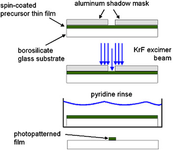
Following spin-coating, a mask was placed on top of the chemically-soluble, solid-state films and the assembly was illuminated with either a 248 nm KrF excimer laser (5 Hz repetition rate, 10 ns pulse) or a 337.1 nm nitrogen laser (5 Hz repetition rate, 800 ps pulse) under ambient laboratory air conditions. Subsequently, the UV-exposed film was washed in pyridine to remove any unreacted film from the substrate. A schematic of this deposition technique (referred to as PSP) is shown in Fig. 1. This process yielded chemically insoluble, photopatterned physical relief structures on the substrates. By contrast, films deposited on the KBr substrates for FTIR spectroscopic analysis were not washed in pyridine following UV-irradiation due to the substrates’ sensitivity to residual water (solubility) in the pyridine (99.0% anhydrous) as well as the amount of time rinsed in pyridine.
Experimental setup for producing photopatterned spin-coated precursor (PSP) films.

C. Direct photodeposition from solution (DPS)
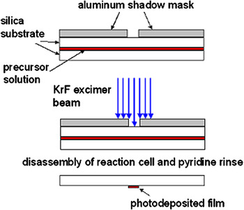
A solution (106 mM) of Ti-TAP dissolved in pyridine was synthesized under dry argon for optical deposition from solution and for subsequent analysis (SEM, stylus profilometry, and FTIR). Films produced for the SEM and profilometry studies were formed from solutions of deionized water (18 MΩ), added to the Ti-TAP solution to create a 4:1 molar ratio of water-to-titanium, and stirred for 30 min. A microliter syringe was used to extract solution (10 μL), which was then deposited onto a fused silica substrate. A second fused silica substrate was placed on top to confine the solution between the two glass layers, effectively creating a deposition cell. A mask was placed on the deposition cell and illuminated with a 248 nm KrF excimer laser (5 Hz repetition rate, 10 ns pulse) in air. The interaction of the laser light with the solution at the interface of the solution and the upper fused silica substrate resulted in the formation of a photodeposited thin film on the substrate. After UV exposure, the cell was rinsed in pyridine to remove any unreacted solution and the deposited film on the upper fused silica substrate was examined. Figure 2 shows a diagram of this deposition technique, termed DPS.
Experimental setup for producing direct photodeposited from solution (DPS) films.

Again, films produced for analysis by FTIR spectroscopy were created using the same general procedure except that the films were photodeposited from solution onto 1-in diameter MgF2 substrates rather than onto fused silica substrates. The MgF2 substrates were chosen for the FTIR analysis not only to provide transparency in the infrared, but also to afford transparency at 248 nm, the wavelength of excitation. Unfortunately, the MgF2 infrared window prevented the acquisition of spectra below 1000 cm−1.
Multiple sample films were produced for both spin-coated solid-state precursor and direct deposition from solution studies. The representative data is shown below in the subsequent sections.
D. Film characterization and modeling
After the PSP and DPS films were generated and dried, they were subsequently characterized by SEM, stylus profilometry, and FTIR spectroscopy. Micrographs were acquired using a Hitachi S-4500 Field Emission Scanning Electron Microscope operated at an accelerating voltage of 15 kV. Prior to use, the thin film samples were coated with platinum to reduce charging effects. Stylus profilometry was performed using a Dektak 6M profilometer with a 12.5 μm radius diamond tip. Infrared transmission spectra were obtained via a Bruker Tensor 27 Fourier Transform IR spectrometer.
Quantum computational modeling was used to predict the specific vibrational modes present in the Ti-TAP molecule using density functional theory (DFT). DFT was performed using the Gaussian 03 software package utilizing the B3LYP hybrid functional and the 6-31g(d) basis set as previously described.Reference Musgraves, Potter, Sewell and Boyle16 Subsequent to energy minimization of the structure, a normal mode analysis was performed to allow comparison with experimentally derived vibrational spectra. While an exhaustive, peak-by-peak analysis of the vibrational spectra was beyond the scope of the present work, the identification of key groupings of resonances associated with the ligand moieties of the Ti-TAP molecule was obtained, enabling the impact of photoexposure on the stability of these structures to be examined.
III. RESULTS
A. Material formation: Vibrational spectroscopy
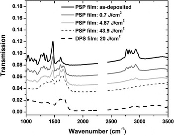
A complete understanding of the photophysics of the ligand structure for both the PSP and DPS processed films is critical to assess the impact of the optical exposures on the material formation processes leading to the final film structure. Figure 3 shows a comparison of FTIR transmission spectra from the as-deposited (not UV irradiated) PSP film and following various accumulated UV irradiation (248 nm) fluences of 0.7, 4.87, and 43.9 J/cm2, respectively, and from a DPS film that was exposed to a total fluence of 20 J/cm2 of 248 nm laser radiation during deposition. The wave number region 2250 to 2500 cm−1 was removed from the data due to the interference from the incomplete removal of atmospheric resonance features. Examination of Fig. 3 reveals that the PSP films exhibited a significant decrease in the peaks located at 1035–1150, 1469, and 2767–2933 cm−1, with increasing irradiation while the intensity of the vibrational peaks located from 1650 to 1700 cm−1 increased in the PSP films with increasing optical exposure. Furthermore, it is interesting to observe that the spectrum of the PSP film irradiated with a fluence of 4.87 J/cm2 exhibits a noticeable decrease in peak heights and a smoothing of peak structure across the spectral range such that it bears strong similarity to the 43.9 J/cm2 PSP spectrum and to the DPS spectrum (20 J/cm2). It is clear that both spectra share the same general features with the DPS spectrum with only minor variations in the resonance features’ intensity in the range of 1000 to 1750 cm−1 and with nearly identical spectral features in the range of 2500 to 3500 cm−1. A summary of select vibrational resonance assignments for Ti-TAP using DFT computations is shown in Table I.
FTIR spectroscopy of an as-deposited PSP film and the effects of 248 nm exposure with optical fluences of 0.7, 4.87, and 43.9 J/cm2. Also shown is a DPS film illuminated with 248 nm light for a total fluence of 20 J/cm2.

Select vibrational resonance assignments.

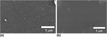
The surface structure of material produced by the DPS and the PSP films was examined via a scanning electron microscope. In this case, both materials were illuminated with a 248 nm laser (10 mJ/cm2/pulse) through a circular aperture with a total fluence of 10 J/cm2. Figure 4(a) depicts the surface of a DPS film consisting of a 4:1 molar ratio of water to titanium.Reference Musgraves, Potter and Boyle19 Nanometer-scale surface roughness with evenly distributed surface porosity (∼10 nm size pores) can be clearly seen in the figure. By contrast, a PSP film, shown in Fig. 4(b), exhibited reduced surface roughness, but contained isolated regions of larger scale porosity (with varying size pores) as a result of unreacted material rinsed away by the pyridine wash.
Nanostructure of (a) DPS film and (b) PSP film exposed to 248 nm light with a total fluence of 10 J/cm2.

B. Photopatterning
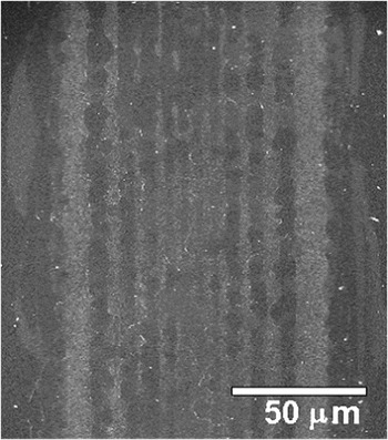
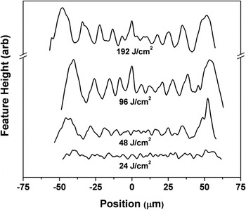
Efforts were made to produce high resolution physical-relief structures using the PSP and DPS deposition techniques. The ability to pattern thin-film structures was investigated using SEM microscopy. Figure 5 depicts an SEM micrograph of a physical-relief structure photodeposited from solution using a 248 nm exposure at 10 mJ/cm2/pulse with a total fluence of 192 J/cm2. The DPS film was photodeposited using a 105 μm single slit aluminum shadow mask placed on top of the deposition cell that contained the Ti-TAP solution with a 4:1 molar ratio of water to titanium. In the figure, it should be noted that the photo deposited film region is confined within the two, thick, pale gray lines in the micrograph such that the bare substrate is depicted outside of those regions. The lighter regions on the photodeposited film image correspond to relative maxima in surface topology height whereas the darker regions correspond to relative minima. Figure 6 depicts an image of this surface topography obtained via stylus profilometry at different points in the photodeposition process as a function of total accumulated UV fluence for the following fluence values: 24, 48, 96, and 192 J/cm2, respectively. The development of the surface structure with increasing exposure can clearly be seen in the figure.
SEM micrograph of the microstructure of a DPS film exposed to 248 nm radiation with a total fluence of 192 J/cm2.

Profilometer trace of the surface topology of a DPS film for four different fluence values: 24, 48, 96, and 192 J/cm2 with an excitation wavelength of 248 nm.

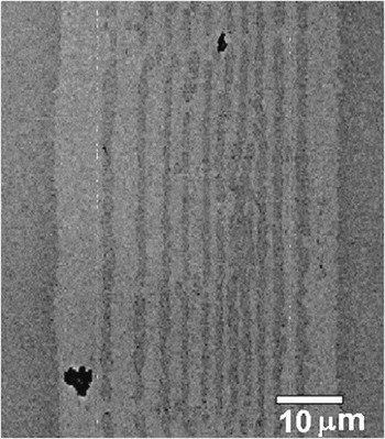
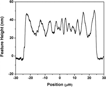
Similarly, PSP films were also examined by SEM following optical irradiation. Figure 7 shows an SEM micrograph of a photopatterned, spin-coated film illuminated through a single slit ∼50 μm aluminum shadow mask. The film received a total fluence of 24 J/cm2 of 248 nm radiation (10 mJ/pulse/cm2). As stated previously, the film was rinsed in pyridine following irradiation to remove any unreacted material. As in Fig. 5, the photopatterned film is located between the two broad light gray lines (outside of those lines is the bare substrate) and the lighter regions represent the relative surface maxima while the darker regions represent the relative minima in height of the surface topology. It should be noted that a larger fluence value was used for the DPS film than the PSP film to demonstrate photodeposited film structure in the SEM micrograph. Figure 8 depicts a profilometry trace of the surface of the film shown in Fig. 7. The photopatterned film of Fig. 8 resembles that of a top hat structure that is ∼50 nm in height with an oscillating height variation. The strong similarity of the photopatterned surface topology of the PSP (Figs. 7–8) and DPS (Figs. 5–6) films is immediately evident.
SEM micrograph of the microstructure of a PSP film exposed to 248 nm radiation with a total fluence of 24 J/cm2 subsequently rinsed in pyridine.

Profilometer trace of the PSP film shown in Fig. 7.

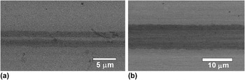
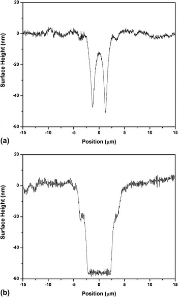
Photopatterning resolution experiments were performed by placing a transparent photomask, which contained a variety of opaque features on the order of 1–10 μm in size, on top of a PSP film and illuminating the sample for a total at-sample fluence of 43 J/cm2 using a 337.1 nm nitrogen laser with a subsequent rinse in pyridine. An excitation of 337.1 nm was chosen due to the transparency of the transmissive regions of the photomask at this wavelength. SEM micrographs, shown in Figs. 9(a) and 9(b), obtained from samples patterned using the shadow mask containing 1–10 μm features, verify the successful photoproduction of physical relief structures from the PSP films. Figures 9(a) and 9(b) show two photopatterned features in which the darker regions coincide with the bare substrate and the lighter regions correspond to the film. The width of the overall features in the micrograph in Figs. 9(a) and 9(b) are ∼3.5 μm (measured from both edges of the darker region) and ∼8.8 μm, respectively. Profilometer traces of these films, shown in Figs. 10(a) and 10(b), were performed and support the data seen in the micrographs. The profilometer traces coupled with the SEM micrograph images affirm the ability to photopattern these PSP films at the micron level. Further optimization of the photopatterning conditions is anticipated to enable the production of submicron scale features.
SEM micrograph of a PSP film illuminated with a 337.1 nm nitrogen laser for a total at-sample fluence of 43 J/cm2. The photomask contained an opaque rectangular feature of (a) ∼5 μm and (b) ∼10 μm.

Profilometer trace, as seen from the SEM micrograph in Fig. 9, of the surface topology of the PSP film after UV illumination of the transparent photomask with an opaque rectangular feature of (a) ∼5 μm and (b) ∼10 μm.

IV. DISCUSSION
It has been previously reported that Ti-TAP is both stable in water and acts as a limiter to conventional hydrolysis kinetics.Reference Musgraves, Potter and Boyle17–Reference Musgraves, Potter and Boyle19 Furthermore, irradiating such solutions with UV light has been shown to cause disruption in the ligand groups resulting in molecular linking through hydrolysis and condensation reactions.Reference Musgraves, Potter and Boyle17–Reference Musgraves, Potter and Boyle19 The resemblance of the vibrational spectra (Fig. 3) of the two film types suggests that the photostructural modification of the Ti-TAP precursor is largely insensitive to the local dynamic environment of the precursor molecule. For the PSP film spectra (Fig. 3), a decrease in most of the sharp vibrational features with increasing fluence was noted. The reduction in the vibrational peaks’ intensity with increasing optical fluence for high (2767 and 2933 cm−1) and low (1035–1150 and 1469 cm−1) resonance frequencies corresponds to disruption in the TAP ligand (Table I). However, the intensity of the vibrational resonance at 1608 cm−1 remained relatively unchanged with increasing irradiation and has been attributed to the OPy ligand, as shown in Table I, from DFT computational calculations. This, therefore, suggests that there is a photoinduced preferential disruption and destabilization of the TAP ligand over that of the OPy ligand. The preferential modification in the TAP ligand allows for hydrolysis and condensation reactions to occur for both of these deposition methods: a DPS technique with the precursor solution containing a 4:1 molar ratio of water-to-titanium as well as a PSP technique with the spin-coated film subject only to atmospheric moisture. Furthermore, for the PSP film, the increase in vibrational intensity in the resonance features, with increasing optical irradiation, for peak positions between 1650–1700 cm−1, has been tentatively identified as an amine-based resonance by comparison with DFT models. This suggests that UV light disrupts and breaks apart the TAP ligand leading to amine-based fragments in the solid-state PSP film. Generally, then, the photodisruption of the ligands allows for photoinduced formation of insoluble, spatially-defined film structures.
While the local environmental conditions sampled by the precursor molecules appear to be ineffective in influencing the intrinsic photophysical response of these precursors, the development of extended structure does appear to be affected, as observed in the film surface structure shown in Figs. 4(a) and 4(b). In these figures, the surface roughness was observed to be typically higher in DPS versus PSP films. The enhanced mobility of the reactants in the solution deposition (DPS technique) likely contributed to the formation of discrete clusters of interconnected, partially reacted precursors upon photoexcitation, thus enhancing the development of a more coarse surface topography as successive layers of partially condensed material, in the form of these clusters, were deposited with each optical pulse. In contrast, precursor molecules in the solid-state (PSP technique) were significantly constrained during the photoexposure process, thus precluding their translational and rotational movement and the probability for close approach of photoactivated ligand sites and bridging bond formation. Coupled with the inability of reacted species to reorient in this environment, it is reasonable to infer that the final, photopatterned material in this case is largely dictated by the initial molecular conformations present in the PSP film, thus limiting the development of larger scale topography with photoexposure. Moreover, the PSP film contained isolated regions of porosity which appear to be the result of unreacted film (presumably due to “cool spots” in the illuminating laser beam) that were washed away in the pyridine rinse. The heterogeneity of the material patterned from the PSP films, when compared to the more evenly-distributed surface porosity of the DSP films, is another effect of the limited precursor mobility in the solid-state system. Thus, in addition to the manipulation of the intrinsic photoexcitation phenomena and the ensuing reaction processes through optical excitation conditions and molecular design, the extended structure of these materials can also be altered via control of the local environmental conditions sampled by the molecules during photoexposure. In this context, the differences in surface topography attainable can be an important distinction between the two deposition techniques for applications (i.e., cellular adhesionReference Riley, DeRosa, Blaine, Potter, Lucas, Le Coq, Juncker, Boesewetter, Collier, Boussard-Pledel and Bureau5) in which surface porosity is a key consideration.
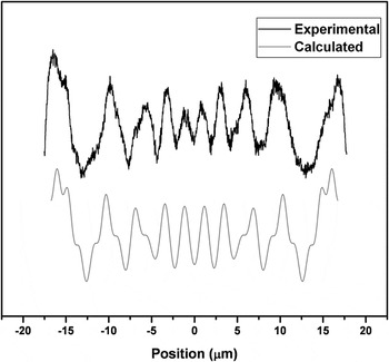
The ability to photopattern physical relief structures directly from solution and from a solid-state spin-coated precursor film was examined and is shown in Figs. 5–8. Immediately obvious is the undulation of the surface profile of the DPS film, seen in the SEM micrograph in Fig. 5, which resembles the intensity variation of a near-field Fresnel diffraction pattern through the single slit shadow mask as previously noted using this deposition technique.Reference Musgraves, Potter and Boyle17 The surface topology of the PSP film, shown in Fig. 8, resembles that of the intensity profile of a near-field Fresnel diffraction pattern as well. Assuming, therefore, that Fresnel diffraction by the slit produced an intensity variation in the illuminating laser beam that was, then, translated into large-scale surface structure in the photopatterned spin-coated film, the anticipated diffraction from the slit was calculated, as previously described,Reference Musgraves, Potter and Boyle17 and compared to the periodicity of the surface topography recorded by profilometry of the film surface. The comparison of the modeled diffraction pattern and the profilometry trace is shown in Fig. 11 with the following parameters: a slit width of 44 μm, a distance of 203 μm between the shadow mask and film, and a wavelength of light of 248 nm. The similarity of the modeled intensity profile of the diffraction pattern and the surface topology of the photopatterned film is clearly seen in the figure. Additionally, the surface topology of the films using both deposition techniques, as shown in Figs. 6 and 8, demonstrated a strong correlation with the anticipated laser beam intensity variation resulting from Fresnel diffraction from the edges of the single-slit aluminum shadow mask. This clearly establishes the impact of optical illumination intensity and fluence on the patterning process and also suggests the capability of photopatterning on a much smaller scale.
The surface topology of a PSP film compared to the intensity profile of the Fresnel diffraction pattern assuming modeling parameters of: 44 μm slit width, 203 μm distance between the shadow mask and film, and 248 nm wavelength of light.

In an attempt to quantify the resolution limit of the photopatterning process in the spin-coated films (PSP), a calibrated, photolithographic photomask was utilized to allow for photoimprinting of micron-size features in the films. Profilometry data of the resulting structures are shown in Figs. 9 and 10. It should be noted that the radius of the profilometer diamond tip was 12.5 μm and thus the smaller features depicted in the profilometry trace of Figs. 10(a) and 10(b) are obscured by the inability of the profilometer stylus tip to reach the unpatterned, bare substrate. This is responsible for the sloped sidewalls evident in Figs. 10(a) and 10(b) and the lack of a flat bottom seen in Fig. 10(a). Moreover, the feature heights depicted in both Figs. 10(a) and 10(b) are not representative of the actual heights of the physical structure due to the tip geometry of the profilometer. The wider feature shown in the image in Fig. 9(b) is clearly depicted by the profilometry trace in Fig. 10(b) showing a feature width of ∼10 μm and a feature depth of ∼56 nm. It should also be noted that an excitation wavelength of 337.1 nm was chosen to photopattern these submicron features due to the transparency of the photolithographic photomask at this wavelength. However, past research has shown a greater photostructural modification at an excitation wavelength of 248 nm than at exposures of 337.1 nm light.Reference Potter, Musgraves and Boyle18 This suggests the possibility to photopattern at an even higher resolution (smaller feature size), potentially leading to sharper features, with an exposure of 248 nm.
V. CONCLUSION
Physical relief structures from oxide-based material were produced by either a direct deposition from solution or from a solid-state, spin-coated precursor film through in situ optical processing. The vibrational structure of both these films were similar and suggests that the optical illumination of the solutions and of the spin-coated films relies on photo-mediated preferential disruption of the TAP ligand leading to hydrolysis and condensation reactions. While the local environment, determined by the deposition technique, appears to be unsuccessful in affecting the vibrational structure between the irradiated solid-state precursor and the photodeposited film, the extended structure (i.e., the surface nanostructure) was seen to be influenced by the different precursor conditions. This is likely due to the variation in reactant-molecule dynamics and optical exposure conditions between solution and solid-state precursor systems.
Furthermore, using an aluminum shadow mask, Fresnel diffraction patterns were observed while photopatterning both types of films, suggesting the potential for high-resolution optical patterning of these materials. In particular, it was shown that feature sizes on the order of ∼1–10 μm could be readily photoimprinted on the solid-state, spin-coated films. The ability to manipulate thin film structures on the microscale and nanoscale by controlling the molecular assembly of units, by various deposition techniques, can be extended to other metal-oxide based systems. The application of theses techniques, then, impacts technologies in which the potential to create insoluble physical relief structures for reproducible production of small feature sizes with in situ optical patterning (i.e., waveguiding structures and gratings) and the ability to control nanostructure through various deposition techniques (i.e., for cellular adhesion) is of great importance.
ACKNOWLEDGMENTS
This research was supported by the United States Department of Energy, Office of Basic Energy Sciences. Partial support was also provided by the University of Arizona, State of Arizona, TRIF Optics Initiative program and by Sandia National Laboratories. Sandia is a multi-program laboratory operated by Sandia Corporation, a Lockheed Martin Company for the United States Department of Energy’s National Nuclear Security Administration under Contract No. DE-AC04-94AL85000.