Introduction
Metal films perforated with an array of sub-wavelength holes have intrigued researchers since the discovery that these arrays show extraordinary transmission of light.[ Reference Ebbesen, Lezec, Ghaemi, Thio and Wolff 1 – Reference Martín-Moreno, García-Vidal, Lezec, Pellerin, Thio, Pendry and Ebbesen 4 ] The enhanced transmission is mediated by surface plasmon polaritons (SPPs) that are excited at the metal surface by diffraction form the array. Arrays of nanoholes find many different applications such as, e.g., in color filters[ Reference Skinner, Talin and Horsley 5 ] nanoscale light concentrators for application in bio-sensors,[ Reference McMahon, Henzie, Odom, Schatz and Gray 6 ] and in solar cells.[ Reference Atwater and Polman 7 , Reference Ferry, Verschuuren, Li, Verhagen, Walters, Schropp, Atwater and Polman 8 ] To realize applications at a large scale, a fabrication method is required that is able to pattern hole arrays with designed geometry, hole size, and pitch at large area and at low cost.
Nanohole arrays in metal films are often made using focused ion beam (FIB) milling of a metal film, or by electron beam lithography in combination with metal lift-off, which are both relatively slow and expensive fabrication techniques. Interference lithography in combination with liftoff is also being used, but is limited to the fabrication of patterns with a fixed period. Moreover, a disadvantage of the metal lift-off procedure is that it often requires the use of a thin (2–5 nm) adhesion layer of titanium or chromium, which strongly absorbs surface plasmons. Furthermore, the lift-off process releases a large density of metal dots, some of which typically adhere to the array, causing imperfect patterns that reduce the optical performance of the array.
Recently, nanoimprint lithography[ Reference Gates, Xu, Stewart, Ryan, Willson and Whitesides 9 , Reference Boltasseva 10 ] was introduced to produce arrays of nanoscale holes in a metal film.[ Reference Kwak, Henzie, Chang, Gray, Schatz and Odom 11 – Reference Yao, Le, Gray, Moore, Rogers and Nuzzo 17 ] While these previous results have been very promising, in some case they resulted in either structures with limited area due to size constrains on the soft-imprint technique, freely floating arrays that are quite fragile,[ Reference Kwak, Henzie, Chang, Gray, Schatz and Odom 11 ] structures in which the holes were not fully continuous through the film,[ Reference Malyarchuk, Hua, Mack, Velasquez, White, Nuzzo and Rogers 12 , Reference Truong, Maria, Yao, Stewart, Lee, Gray, Nuzzo and Rogers 14 ] or structures with limited control over the hole geometry because a self-assembled colloidal mask was used.[ Reference Lee, Bantz, Lindquist, Oh and Haynes 16 ]
Here we introduce an alternative soft-imprint procedure to produce large-area sub-wavelength nanohole arrays. Our substrate-conformal imprint lithography (SCIL) technique uses a composite soft stamp composed of a high-Young's modulus poly-di-methyl-siloxane (PDMS) layer that contains the pattern, laminated to a soft PDMS layer on a soft glass plate,[ Reference Odom, Love, Wolfe, Paul and Whitesides 18 ] and allows for wafer-scale patterning of sub-50 nm features with very low distortions.[ Reference Verschuuren and van Sprang 19 , Reference Verschuuren, Megens and Polman 20 ] The SCIL technique can be used to realize conformal patterns over areas as large as a 15 cm-diameter wafer. We use SCIL to fabricate an array of silica nano-pillars that is then coated with gold, whereupon the silica is chemically dissolved. In this way, hole arrays with a predefined pattern are achieved, free of scattering particles or defects. Optical transmission spectrometry is presented that demonstrates the high optical quality of the imprinted nanohole arrays. By optimizing the imprint procedure metal hole arrays with a symmetric dielectric environment are achieved, that show further optimized extraordinary transmission characteristics.
Fabrication of nanohole arrays using soft-nanoimprint lithography
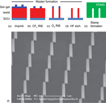
As a master pattern for the soft stamp a square array of 150-nm-diameter dots at a pitch of 780 nm was made in a thick hydrogen-silses-quioxane (HSQ) layer on Si using 100-keV electron-beam lithography (total area 0.5 × 0.5 mm2). After the development of the HSQ the surface of the master pattern is made non-reactive by applying a monolayer of a fluoro-silane by vapor phase deposition.[ Reference Jung, Li, Wu, Chen, Olynick, Wang, Tong and Williams 21 ] A double-layer PDMS rubber stamp[ Reference Schmid and Michel 22 , Reference Odom, Love, Paul, Wolfe and Whitesides 23 ] was then molded from the master. Next, we use this stamp to create a second master pattern with the same pitch and diameter, but with higher aspect ratio structures. This process is schematically indicated in Figs 1(a)–1(e). First, a silicon wafer was sputter-coated with a 50 nm-thick layer of chromium after which a ~1 µm-thick layer of HPR-504 positive photoresist was applied by spin coating. This layer was baked for 30 min on a hot-plate at 250 °C, after which a ~700 nm-thick cross-linked resist layer remains. On top of this layer a precise amount of silicon sol–gel imprint resist[ Reference Verschuuren and van Sprang 19 ] is applied by spin coating. Directly after spin coating, the first stamp molded from the HSQ dots is applied in the sol–gel resist. After 30 min, the sol–gel resist has formed a rigid silica-like material and the stamp was removed by gentle pealing, leaving the silica structure as shown in Fig. 1(a). The residual sol–gel layer under the feature was removed by a CF4/N2 anisotropic reactive ion etch (RIE). The remaining sol–gel resist serves as a mask during a subsequent oxygen RIE etch of the organic resist layer. The remaining sol–gel etch mask is then removed using a 1 wt% hydrofluoric acid (HF) solution. Figure 1(f) shows a scanning electron microscope (SEM) image of the resist pillars. The 600 nm-tall pillars are straight, have smooth side walls and are uniform in height and diameter.
(a–e) Schematic representations of the process steps used to obtain high-aspect-ratio silica pillars; (f) SEM image taken under an angle of ~40° of high-aspect-ratio resist pillars used to fabricate the master. Scale bar is 1 µm.

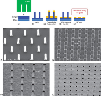
Next, this high-aspect-ratio resist pattern is used as a master to mold a second composite soft PDMS stamp that is used to produce nanohole arrays in a gold film. Figures 2(a)–2(e) show schematic representations of the process steps. SEM images of the different stages of the fabrication of the nanohole array are shown in Figs 2(f)–2(i). A ~100 nm-thick sol–gel layer spin-coated on an AF45 glass substrate is first imprinted with the second stamp. After the sol–gel has solidified, the stamp is carefully removed, leaving an array of silica pillars, which are then cured in an oven at 200 °C in air. Figure 2(f) shows an SEM image of the resulting 650 nm-tall silica pillars. Figure 2(g) shows the sample after gold is deposited over the pillars by sputter deposition to a nominal thickness of 250 nm. The actual amount of gold deposited on the pillar sides is about 100 nm, judging from the increased pillar diameter in Fig. 2(g). Next a thio-urea/iron-sulfate based wet etch is used to remove the metal from the pillar top and side walls.[ Reference Burdinski and Blees 24 ] This mixture has an etch rate on flat sputtered gold of ~32 nm/min at room temperature. Figure 2(h) shows the sample after 3 min of wet etching and clearly shows that all the metal is removed from the pillar sides as well as the top of the pillar. The short etch time required to remove all the metal from the pillars is attributed to porosity of the metal on the pillar sides and the high surface-to-volume ratio of the (250 nm-thick) metal on top of the pillar. The wet etch removes ~120 nm from the planar metal layer, leaving a ~130 nm-thick gold layer with holes at the pillar position. The sol–gel pillars are then removed by a short etch in 1 wt% HF. Figure 2(i) shows the gold nanohole array after the sol–gel pillars are removed. The SEM image clearly shows that the square array is well reproduced. The hole diameter is enlarged to 180 nm compared with the initial diameter of the sol–gel pillar [Fig. 2(f)], which we attribute to a combination of shadow effects during sputter deposition and the removal of metal by the wet gold etch. Replicating thinner pillars would allow to decrease the hole diameter further if desired. The stamp used to fabricate the arrays can be used at least 500 times.
(a–e) Schematic representation of the process steps used to obtain hole arrays in Au; SEM images at different stages in the nanohole array fabrication taken under an angle of ~40°: (f) imprinted sol–gel pillars; (g) imprinted sol–gel pillars after sputter coating with 250 nm gold; (h) the metal is removed from the pillars and a hole array remains with ~500 nm-high silica pillars protruding from the holes; (i) silica pillars are removed by etching in the diluted aqueous HF. All scale bars are 1 µm.

The procedure described above leads to a metal hole array on a glass substrate, i.e., an asymmetric dielectric environment (referred to as sample A). We also studied the fabrication of array geometries with a more symmetric dielectric surrounding as it is known that this enhances the optical transmission through the array. To do so, we used the same procedure as shown in Fig. 1, fabricating a sample in which the sol–gel pillars were left un-etched, thus leaving the holes in the metal filled with sol–gel (sample B). In a third geometry, after the last etch step, Fig. 2(i), a 340 nm thick sol–gel coating was applied on top of the array (sample C). This layer fills up the holes and a uniform sol–gel layer on top the array is formed with a refractive index of n = 1.42, as measured on a planar substrate using ellipsometry. Finally, a fourth geometry was made by first coating the AF45 glass substrate (refractive index n = 1.54) with a 2 µm-thick sol–gel layer. On this sol–gel layer the gold hole array was defined using the same procedure as above, followed by overcoating with a ~2 µm-thick sol–gel layer. This then leads to a symmetric dielectric surrounding with index n = 1.42 on both sides of the metal hole array (sample D).
Optical characterization of nanoholes arrays
Angle-resolved optical transmission spectra were measured for hole arrays with the four different dielectric surroundings. An incandescent lamp was coupled to a 200-μm-diameter multimode fiber of which the output was focused to a ~300 µm-diameter spot on the sample. The transmitted light was sent to a fiber-coupled grating spectrometer. For visible to near-infrared wavelengths (500–1000 nm) we used a charge-coupled device detector (resolution 1.2 nm). For near-infrared wavelengths (900–1700 nm) we used an InGaAs array (resolution 3 nm). The numerical aperture of the incident and transmitted light beam was less than 0.01. Polarizers were placed in parallel parts of the incident and transmitted beams. The substrate was placed onto a rotation mount with the rotation axis aligned with the (0,1) direction of the hole array. The wave vector and polarization of the incident light were perpendicular to this direction (p-polarization).
Figure 3 shows transmission spectra at normal incidence for the four different hole arrays with 180 nm diameter holes at a pitch of 780 nm in a ~130 nm-thick gold film: (a) a hole array on AF45 glass as in Fig. 2(i); (b) a hole array with sol–gel pillars protruding from the holes; (c) a hole array on glass with a 340 nm sol–gel on top; and (d) a hole array surrounded by ~2 µm-thick sol–gel layers. The transmission is normalized to the transmission measured on an area where no metal is present. As can be seen from Fig. 3(a) the hole array exhibits several clear transmission peaks, corresponding to the (1,0) and (1,1) SPP modes at the air side of the array and the (1,0), (2,0), and (1,1) modes at the glass side of the array. The transmission features are similar to those observed earlier for hole arrays made with e-beam lithography, indicating that the soft imprint technique presented here leads to well-defined hole arrays of good optical quality.
Optical transmission spectra of a square array of 180 nm-diameter holes with a 780 nm pitch in a ~150 nm-thick gold film measured normal to the gold array. (a) Hole array with air on top, (b) hole array with sol–gel pillars protruding from the holes, (c) hole array on glass with a 340 nm sol–gel on top, and (d) hole array embedded in ~2 µm-thick sol–gel layers.

Leaving the silica pillars inside the holes [sample B, Fig. 3(b)] leads to small variations in the transmission spectrum that result from the increased refractive index inside the holes. Most pronounced in Fig. 3(b) is the strong reduction of the (1,1) air mode, the broadening and redshift of the (2,0) glass mode, and the increase of the sharp (1,1) glass modal peak to nearly 4%. Covering the hole array with a thick sol–gel layer [sample C, Fig. 3(c)] leads to a strong redshift of the original (1,0) and (1,1) air modes. The fact that these modes do not fully overlap with the (1,0) and (1,1) glass modes is due to the slight asymmetry in refractive index between the two sides of the metal hole array (index sol–gel silica n = 1.42 and index AF45 glass n = 1.52). This asymmetry is removed in Fig. 3(d) which shows the transmission spectrum for the fully symmetric case (sample D). Three main peaks corresponding to the (1,0), (1,1), and (2,0) glass modes are observed indicating the dielectric layers on both sides are well index-matched. The peaks have broadened significantly and in particular for the (2,0) and (1,1) modes the transmission is strongly increased. The peak transmission for the (2,0) mode is 7.1%. Comparing this value to the geometrical surface area of the metal holes of 4.2%, we find an extraordinary transmission coefficient of 170%. The broadened and increased transmission indicates that coupling between SPPs on either side of the array is strongly increased.[ Reference de Dood, Driessen, Stolwijk and van Exter 25 ] Finally, we note that the main peaks in Fig. 3(d) show strong oscillations with a free spectral range of ~10 nm; these correspond to Fabry–Perot resonances in the 2 µm-thick top sol–gel layer.
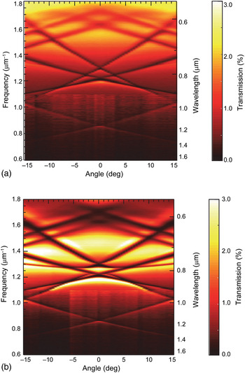
To further study the origin of the transmission minima and maxima and the fine structure in the spectra we investigate the angular dependence of the transmission spectra. Figures 4 and 5 show intensity plots of the transmission as a function of angle of incidence and wavelength for samples A–D. Overall, the dispersive behavior characteristic for metal hole arrays[ Reference van der Molen, Klein Koerkamp, Enoch, Segerink, van Hulst and Kuipers 26 ] is clearly observed in all geometries, testifying of the high optical quality of the soft-imprinted arrays. The minima and maxima in the transmission spectra are caused by Fano-resonances of directly transmitted light and SPP-mediated transmitted light. The different slopes of the dark bands correspond to the different dispersion on the glass side and air side of the metal hole array.[ Reference Stolwijk, Driessen, Verschuuren, ‘t Hooft, van Exter and de Dood 27 ] The modal index found for the modes on the glass substrate side is found to be 1.54, in agreement with the refractive index of AF45 glass. The well-separated dispersion curves in Figs 4(a) and 4(b) clearly reflect the asymmetrical dielectric environment of the arrays. Figure 4(b) shows that the presence of the sol–gel pillars inside the holes strongly increases the transmission of the hole array over the entire angular range. This is ascribed to the increased effective optical cross-section of the hole as the index is increased, in combination with the waveguiding effect of the sol–gel pillars.[ Reference Stolwijk, Driessen, Verschuuren, ‘t Hooft, van Exter and de Dood 27 ]
Angular optical transmission spectra of a square array of 180 nm diameter with a pitch of 780 nm in a ~150 nm-thick gold film. (a) Hole array with air on top and (b) hole array with sol–gel pillars protruding from the holes,

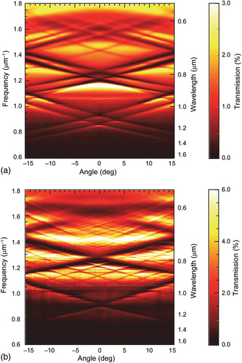
Angular optical transmission spectra of a square array of 180 nm diameter with a pitch of 780 nm in a ~150 nm-thick gold film. (a) Hole array on glass with a 340 nm sol–gel on top, and (b) hole array embedded in ~2 μm-thick sol–gel layers..

Figure 5(a) shows the angle-resolved transmission spectra for the hole array covered with a 340 nm-thick sol–gel layer [sample C, Fig. 3(c)]. Sets of two split dispersive modes are clearly visible, indicating that this sample is not fully index-matched. The effective index of the Au/sol–gel/air mode is found to be n = 1.4, which is slightly lower than that for the sol–gel because the evanescent tail of the SPP mode partially extends into air. Besides the broad transmission minima caused by Fano interference the spectra also contain more narrow transmission minima for wavelengths below 950 nm. We attribute these lines to transverse electric waveguide modes in the top sol–gel layer.[ Reference de Dood, Driessen, Stolwijk, Exter, Verschuuren and ’t Hooft 28 ]
Figure 5(b) shows the transmission data for the metal hole array embedded in sol–gel layers of ~2 µm thickness on either side [sample D, Fig. 3(d)]. As can be seen from the transmission minima, this geometry exhibits no splitting of the equivalent SPP modes, reflecting complete index matching. The strongly enhanced (1,0) and (1,1) modes [see Fig. 3(d)] are clearly seen and show a relatively flat dispersion. A large number of waveguide modes are observed, propagating in the 2 µm-thick dielectric layer. As Fig. 5(b) shows, index matching of the metal hole arrays strongly increases the transmission. For further optimized transmission, the thickness of the sol–gel layers can be optimized, so that coupling to waveguide modes is suppressed at the wavelengths of interest.
Conclusions
We have demonstrated a novel method to fabricate high-quality gold nanohole arrays (180 nm diameter, 780 nm pitch) using a cost-effective soft-nanoimprint method. Using a sequence of soft-imprint processes in combination with evaporation of gold, nanohole arrays are made with both asymmetric and symmetric dielectric surrounding. The arrays show optical transmission resonances and dispersive bands corresponding to the excitation of SPPs on either side of the array. For the fully index-matched array an anomalous transmission of 170% is found at a wavelength of 850 nm. This work shows the potential of the SCIL soft-imprint technique to fabricate metal nanoholes. It may be further expanded to the fabrication of more complex geometries with exciting optical properties.[ Reference Klein Koerkamp, Enoch, Segerink, van Hulst and Kuipers 29 , Reference Kroekenstoel, Verhagen, Walters, Kuipers and Polman 30 ] As the SCIL process can be applied to fabricate nanostructures at 15 cm-diameter wafer scale, this work opens the way to large-area application of metal hole arrays.
Acknowledgments
We thank Ewold Verhagen for useful discussions and insights. The AMOLF part of this work is part of the research program of FOM which is financially supported by NWO. It is also supported by the European Research Counsel and by NANONED, a nanotechnology program of the Dutch Ministry of Economic Affairs.