


1. INTRODUCTION
The civilian and military demands for high power microwaves (HPMs) stimulate the development of relevant technologies, such as pulse power technologies, HPM source technologies, and radiation technologies (Dorranian et al., 2005; Liu et al., Reference Liu, Zhan, Zhang, Liu, Feng, Shu, Zhang and Wang2007; Li et al., Reference Li, Yuan, Zhang, Shu and Zhang2008, Reference Li, Liu, Xu, Chen, Chang, Wan and Wen2009a). There are numerous applications of HPMs in material processing, plasma heating, and environment improving (Barker et al., 2001; Thumm & Kasperak, Reference Thumm and Kasperak2002; Hong et al., Reference Hong, He, Wen, Du, Teng, Qing, Huang, Huang, Liu, Wang, Huang, Zhu, Ding and Peng2009), among others. In recent years, benefiting from the rapid development of pulse power technologies (Liu et al., Reference Liu, Cheng, Qian, Ge, Zhang and Wang2009; Kovalchuk et al., Reference Kovalchuk, Kharlov, Zherlitsyn, Kumpjak, Tsoy, Vizir and Smorudov2009; Mao et al., Reference Mao, Zou, Wang, Liu and Jiang2009; Cheng et al., Reference Cheng, Liu, Qian and Zhang2009), electron emitter technologies (Li et al., Reference Li, Liu, Cheng, Chang, Wan and Wen2009b, Reference Li, Liu, Cheng, Xu, Ge and Wen2009c), and so on (Wang et al., Reference Wang, Lu, He, Zheng and Zhao2009; Aria et al., Reference Aria, Malik and Singh2009), HPM sources generating narrow-band HPMs (Korovin et al., 2003) have been developed extensively. Efforts have also been made on increasing the output power, pulse duration, and conversion efficiency of these devices. However, one of the key issues is that the internal breakdown in these devices limits their power-handling capacities, when the peak power of the microwave increases (Zhang et al., Reference Zhang, Zhong and Luo2004). One method for increasing the power handling capacity of a HPM device is to increase the diameter of its cross-section to several times the free-space wavelength of the generated microwave and consequently reduce the reversed fields in the HPM device for the same power flow. The oversized approach has been successfully used to increase the power-handling capacities of slow-wave HPM devices. Important examples of overmoded devices are the multi-wave Cerenkov generator (MWCG) developed by Bugaev et al. (1990a), the relativistic diffraction generator (RDG) developed by Bugaev et al. (1990b), the relativistic backward-wave oscillator (RBWO) developed by Abe et al. (Reference Abe, Carmal, Miller, Bromborsky, Levush, Anatonsen and Deslter1998), and the surface-wave microwave oscillator developed by Vlasov et al. (Reference Vlasov, Shkvarunets, Rodgers, Carmel, Antonsen, Abuelfadl, Lingze, Cherepenin, Nusinovich, Botton and Granatstein2000). Although significant improvements have been achieved by using overmoded structures to reduce the internal reversed electric fields in HPM devices, there are still other issues that need to be investigated.
However, limited by material technology, the overmoded approach for enhancing the output capacity of HPM sources has its physical limit. Another direct method for enhancing the output capacity of HPM sources is taking advantage of incoherent power combining of several HPM sources (Li et al., Reference Li, Yuan, Zhang, Shu and Zhang2008). Diplexer is such a kind of device, which can be used as a combiner. Usually, diplexer consists of two filters (Fig. 1). Each filter is designed for a narrow-band microwave source, thus, for the simultaneous operation of HPMs, filters employed in the diplexer have their pass band of about 100–200 MHz, and the central frequencies of the filters are the operation frequencies of the narrow-band HPM sources. As the overmoding ratio of the operating waveguide in the X band HPM sources for combining is 12.7, there exist 12 modes, which give difficulties for the design of the combiner. This paper focuses on how to design the X band high power combiner based on overmoded HPM sources, that is, the methods for enhancing the transmission efficiency and power handling capacity, and suppressing the unwanted higher order modes.
(Color online) Sketch of a conventional diplexer (1) filter; (2) metal inserts; (3) tapers; and (4) output waveguide.

Another diplexer with output frequency of L/X band gigawatt level HPMs has been studied by Li et al. (Reference Li, Yuan, Zhang, Shu and Zhang2008). In the diplexer, a set of thin irises is placed in it to transmit and reflect the required microwaves, thus, the dual band microwaves have the same radiation direction. This set of irises is actually a kind of metallic periodic structure, that is, a kind of metallic photonic crystal. Photonic crystal is drawing more and more attention because they may behave like negative refractive index materials (Pendry, Reference Pendry2001) within a certain frequency range. Agi et al. (Reference Agi, Moreland, Schamilogu, Mojahedi, Malloy and Brown1996) presented an application of photonic crystal to a 450 MW HPM, which stands for the early work investigating the applications of photonic crystal to HPMs. Kamil's work demonstrated the frequency selective properties of photonic crystal with HPMs. However, for the application of dual channel gigawatt level X band HPMs, it is necessary to investigate both the stop and the pass properties of a single photonic crystal, thus, the reflection and transmission of the required gigawatt level dual channel microwaves can be realized simultaneously. However, as the gap between the adjacent irises is much smaller than that of the L/X band diplexer, the microwave breakdown problem cannot be neglected anymore according to the experimental results.
In order to solve the breakdown problem, we analyze the photonic crystal applied to X band dual channel gigawatt level HPMs with mode matching and finite difference time domain (FDTD) methods. As illustrated in Figure 2, in the X band, the incident wave is TE polarized (the electric field is perpendicular to the XOZ plane), or TM polarized (the magnetic field is perpendicular to the XOZ plane). With the expansion of incident waves and the application of boundary conditions, the field distributions are obtained with the mode matching method. Then this structure is analyzed by the FDTD method to make a comparison of the numerical results. In the next step, an optimization of the photonic crystal is carried out with the mode matching method, and then validated with the FDTD method. Then, the numerical results obtained from these two numerical methods are discussed together with the experimental results.
Schematic display of photonic crystal applied in HPM system.

Finally, the two methods for enhancing the output capacities of X band microwaves based on overmoded HPM sources are discussed together. Some methods for enhancing the efficiency and power handling capacity are proposed according to the theoretical and experimental results.
2. ANALYSIS
As demonstrated in Figure 3, the slow wave structure cause the microwave to propagate as surface wave, which makes the TM01 mode grows much faster than any other axisymmetrical mode like TMon. Therefore, modern HPM sources generate TM01 circular modes usually.
(Color online). Cross-section of a HPM system based on back wave oscillator. (1) Gas-gap switch for primary storage capacitor. (2) High voltage pulse transformer. (3) Main switch. (4) Intense electron-beam accelerators based on strip spiral Blumlein line. (5) Cathode. (6) Relativistic electron beam. (7) Slow wave structure.

As a result, antennas with the following properties are needed: First, they should be capable of transforming the output TM01 mode into TE11 circular mode or TE10 rectangular mode. Second, they should be capable of transforming the output wave front into a plane-wave front. In this paper, the filters and photonic crystal are investigated assuming that TE10 waveguide modes or linearly polarized plane-waves are incident.
2.1. Diplexer Based on Filter
Figure 4 shows the field distribution of a filter designed with a standard waveguide (22.86 × 10.16 mm2). It is obvious that the maximum electric field exceeds the vacuum breakdown threshold of 1 MV/cm, when the incident power is set to 1 GW. Thus, oversized waveguide should be employed. However, the application of oversized waveguide raises the risk of higher order modes. Therefore, it is necessary to analyze the filters with mode matching method (Reiter & Arndt, Reference Reiter and Arndt1995) to suppress the higher order modes.
(Color online). Field distribution of a filter based on standard waveguide.

Figure 5 gives the schematic display of a section for the microwave filter employed in our diplexer. On the plane Z = 0, the scattered wave is represented by a series of discrete wave, which could be regarded as a representation of all considered higher order modes. The incident wave (FI, BII, BIII, BIV) and reflected wave (BI, FII, FIII, FIV) are expanded by a series of TEm0 modes, which are excited by the discontinuities. FI, BII, BIII, BIV, BI, FII, FIII, FIV are vectors, whose elements stand for the amplitude of the higher order modes. By employing the boundary conditions on the plane Z = 0, we have


A section of microwave filter.

Where the elements of the coupling matrix are given by (here the first coupling matrix is given as an example)

The factor G1 and the wave number of the TEm0 mode are as follows


Where v = 1, 2, 3. Then the general scattering matrix (GSM) on the plane Z = 0 can be evaluated from Eqs. (1)–(7). Because the filter section is symmetrical, the GSM on plane Z = l is the same as it is on plane Z = 0. By cascading the matrixes, the GSM of this filter section can be derived. Therefore, as the GSM of the total filter. At last, a filter with high transmission efficiency is synthesized.
However, in filters, the main waveguide is oversized: a = 46 mm, waveguide height b = 55 mm, a 1 = a 2 = a 3 = 14.4 mm, thickness of the metal insert t = 1.4 mm. Under this situation, the higher order modes at the Y-junction may lead to the reduction of the transmission efficiency and power handling capacity. In order to suppress the higher order modes, the tapered impedance transformer is employed to reduce the width of the main waveguide to 30 mm. As a result, the higher order modes become evanescent modes at the junction, and the transmission efficiency of TE10 mode can be enhanced greatly. The final design of the diplexer has the transmission efficiency above 99.0% in the pass band 9.2–9.4 GHz and 9.5–9.7 GHz. The maximum electrical that appears in the small waveguide formed by the metal inserts field is 622 kV/cm, the field at the Y-junction of the diplexer is within 311 kV/cm, when the incident wave is 1 GW (Fig. 6). Therefore, according to the calculation results, the power handling capacity is as high as 2.58 GW for each channel. The total output capacity will be 5.16 GW.
(Color online) Field distribution of the designed diplexer.

In addition, as illustrated by Eq. (7), the wave number of the TEm0 mode is determined by the width of the specified waveguide section and the mode index m, however, it has nothing to do with the height of the diplexer. Moreover, all the discontinuities in the diplexer are E-plane discontinuities, only TEm0 modes can be excited. Therefore, the height of the diplexer can be adjusted to reduce the reversed field inside the HPM diplexer, without any influence on the transmission properties. For example, if the height of the diplexer is enlarged to 82 mm, the maximum electric field is reduced to 462 kV/cm (Fig. 7), which results in the enhancement of the output capacity from 5.16 GW to 9.35 GW.
(Color oline) Field distribution of the designed diplexer.

2.2. Diplexer Based on Photonic Crystal
Figure 2 shows the structure of the theoretical model of the irises, which form a photonic crystal. For theoretical analysis, the irises can be treated as infinitely long in the X-direction, and periodically spaced in the Y-direction. The thickness of the irises is determined by the value of 2(h-a), where 2h is the period of the irises and 2a is the space between irises. The depth of the irises is w. φ0 is the incident angle of the microwaves.
2.2.1. Analysis with Mode Matching Method
As shown in Figure 2, the polarization of the electric field is perpendicular to the XOZ plane, and the photonic crystal is infinite long in the X direction. In this situation, the scattered wave can no longer be considered as TE or TM wave individually. Namely, the cross coupling of the TE and TM scattered waves should be taken into account. For this reason, we would like to use the plane wave expansion based mode matching method to make a new derivation of the equations for the photonic crystal applied to gigawatt level HPMs. Here, the TE case is given as an example for the analysis. As the incident electric field is perpendicular to XOZ plane and the photonic crystal are infinitely long in the X-direction, and there is no discontinuity in the X-direction, the wave number for the X-direction is a constant for both incident and scattered microwave. The electric and magnetic field of the incident wave is given as follows (Yasumoto, Reference Yasumoto2006)


In accordance with Floquet's theorem (Helfert & Pregla, Reference Helfert and Pregla1998), the reflected and transmitted fields are each the sum of discrete plane-wave harmonics, called Floquet or spatial harmonics; indeed, it is this property of the fields, which motivates the use of a spectral approach with respect to the direction of periodicity. A convenient and useful way to express the solution of a problem is by giving the coefficients of these harmonics, often referred to as the scattering parameters. These parameters include the reflection and transmission coefficients, which are, respectively, the coefficients of the specularly reflected and forward scattered Floquet harmonics. The reflection and transmission coefficient is evaluated here for the structures of Figure 2.
The Borgnis function, with which all the electromagnetic components can be derived, of reflected wave is given by


Therefore, the tangential field of reflected wave can be expressed as


The Borgnis function of transmitted wave is given by


Therefore, the tangential fields of transmitted wave are


Where the Floquet propagation constants in the X-, Y- and Z- directions (m = 0, ± 1, ± 2…) are given by


Considering periodic properties, the electromagnetic fields in the strip region (0 ≤ z ≤ w) may be expanded in terms of waveguide modes, the Borgnis functions of these waveguide modes are



Where


Just as the procedure for deriving the above electromagnetic fields from Borgnis functions, the electromagnetic fields in between the strip are given by (here the detailed expressions are not given)


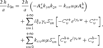
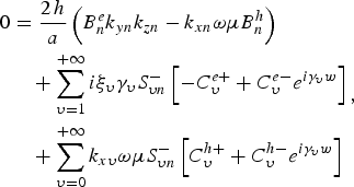
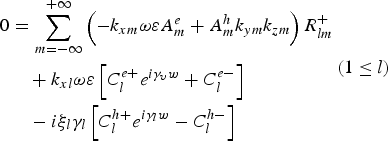
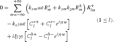
The above-mentioned A m, B m, and C m are all unknown coefficients. Floquet's theorem predicts that the scattered fields will have a discrete plane-wave spectrum and that it is sufficient to determine the fields and fields in a single unit cell because the fields elsewhere will be related to those in the principal cell by a phase shift. Taking into account the continuous conditions of the tangential components of electromagnetic fields cross the boundary planes at z = 0 and z = w between the gap –h ≤ y ≤ h (which is defined as principal cell), we can get the following simultaneous equations for the unknown coefficients
Where


Here the continuous equations for the Y-components of the electromagnetic fields are given. The study of field distributions on photonic structures requires the use of many basis functions as these functions do not take into account any knowledge of the structure or field distribution. It was found that on the order of 30 basis functions per wavelength for the structure of Figure 2 are needed for convergence. This leads to large mode matching matrix sizes. More basis functions are added to more accurately model of the field distribution. Thus, more terms must be included in the summation over the Floquet harmonics in each element of the mode-matching matrix. By solving the linear simultaneous equations, the unknown magnitude of the scattered and transmitted wave can be obtained, as well as the field distributions.
For the case of TM incidence, we want to realize the reflection of the X band microwave; thus, the dual channel microwaves share the same radiation direction. In the calculation, the polarization of magnetic field is in the Y direction of Figure 2. As a result, for a linearly polarized plane wave, the polarization of the electric field is parallel to the XOZ plane; if the distance between irises is smaller than half the wavelength of the X band microwave, it will be reflected. Because the Borgnis function for the scattered and transmitted wave remains the same for the case of TM incidence, as a result, the deduction of TM incidence is the same as the deduction of TE incidence, except the left side of Eq. (17a), which stands for the incident terms.
2.2.2. Analysis with FDTD method
To validate the numerical results obtained by mode matching method, another program based on the FDTD method has been developed. Over the past decades, a range of computational methods have evolved to model photonic crystal structures including FDTD methods (Taflove & Brodwin, Reference Taflove and Brodwin1975), transfer matrix methods (Meade et al., Reference Meade, Rappe, Brommer and Joannopoulos1993), finite element methods (Li & Lin, Reference Li and Lin2003), and so on. Of all these methods, FDTD has been proved to be a rigorous computational electrodynamics modeling technique, and thousands of scientific papers on this method have been published, ever since the basic FDTD space grid and time-stepping algorithm was developed by Yee (Reference Yee1966).
The parameters of the model employed to calculate with FDTD method are identical as what are shown in Figure 2, except the length of the photonic crystal is set to be 1 m. In the calculation, h = 9.5 mm, a = 8 mm, w = 20 mm. Figure 8 shows that both method provide a fairly good agreement with each other, even though the length of the photonic crystal employed in FDTD are not infinite long. However, the FDTD model is the practical model applied in the experiments.
(Color online) Field distribution of y-component of electric field in between the principal cell (between z = 0 and z = w, in the gap –h ≤ y ≤ h).

Without the calculating of the time-domain field distribution at each lattice, the mode matching method provides a faster calculation for this issue. In this sense, the mode matching method turns out to be more efficient for the analysis and optimization of this model. However, because the FDTD method is a rigorous method and can be applied in a wider range, in this part, we use mode-matching method as an optimization method for the primary design of the photonic crystal. The goal of this optimization is to maximize the reflection efficiency and transmission efficiency with equal weight factor for the dual channel X band microwaves. After the optimization, the model is calculated with FDTD method for validation of the mode matching method.
Noticing that the transmission efficiency and the reflection efficiency in steady-state are constant when they are calculated by the FDTD method, we integrate the fields to get the powers of the incident waves, and the scattered wave in-between the irises. Then we can obtain the transmission efficiency of the TE and TM polarized microwave separately. For the transmission of the TE polarized microwave, the transmission efficiency is expressed as

For the reflection of the TM polarized microwave, the reflection efficiency cannot be given directly by the FDTD method. If we consider the metal photonic crystal to be lossless, the reflection efficiency is given by,

The calculation results reveal that the transmission efficiencies of TE wave calculated by mode matching method and FDTD method are 99.80% and 99.08%, respectively; the transmission efficiencies of TM wave calculated by mode matching method and FDTD method are 99.61% and 99.14%, respectively, which once more demonstrate the good agreement of both methods.
The grid spatial discretization in the FDTD calculation must be sufficiently fine to resolve both the smallest electromagnetic wavelength and the smallest geometrical feature in the model. As a result, the grid numbers should be large enough for both channels of microwaves with acceptable time consumption. In our calculation, the grid dimension in X, Y, Z direction are 3 mm, 1 mm, and 1 mm, respectively, the snapshots of the field distributions are displayed in Figures 9–12.
(Color online) Snapshot of the electric field distribution on XOZ at 9.6 GHz, TE incidence.

(Color online) Snapshot of the electric field distribution on YOZ at 9.6 GHz, TE incidence.

(Color online) Snapshot of the electric field distribution on XOZ at 9.6 GHz, TM incidence.

(Color online) Snapshot of the electric field distribution on YOZ at 9.6 GHz, TM incidence.

As shown in Figures 9 and 10, the TE polarized microwave is transmitted by the photonic crystal without fatal attenuation. Figures 11 and 12 show that the TM polarized microwave is not transmitted by the photonic crystal, it has been reflected. This is a further demonstration of the mode matching method.
Up to now, the diplexer base on photonic crystal is analyzed theoretically. However, according to the previous analysis, the cross-polarization issue can not be neglected. To reduce the high cross-polarization of the element, a special crystal configuration for the array, containing columns with an even number of elements, is considered. The configuration uses elements that are located symmetrically about the column's Y-axis. Mirror-image symmetrical transition lines with equal amplitudes and a 180° phase difference excite any pair of symmetrically located elements. The amplitude of any pair can be arbitrarily selected. One side of the pair now produces the cross-polarization, which cancels the cross-polarization of the other side of the pair. This arrangement can be used for any array with an even number of elements. The proposed arrangement is very versatile, and various modifications can be used according to system requirements.
Arranging the photonic crystal with such a method, the cross polarization is minimized according to the calculation results of mode matching method and FDTD method. Also taking the TE polarized incidence as an example, with h = 9.5 mm, a = 8 mm, w = 20 mm, the X-component of the cross polarized electric field has a magnitude of 10−5 V/m level, and Z-component of the cross polarized electric field has a magnitude of 0.12 V/m level on the plane z = 0, when the incident electric field is 1 V/m. That is to say, the cross-polarization levels are very low. And what is more, according to Eq. (13c), the higher-order space harmonics are all evanescent modes, because Kz(1), Kz(2), Kz(3) et al. are all imaginary. As a result, within several wavelengths, all higher order space harmonics (1, 2, 3…) of scattered and transmitted wave will fade down.
3. EXPERIMENTS
Both methods for enhancing the output capacity of X band HPMs are needed to be validated by low power and high power experiments. The low power tests are intended to measure the transmission efficiency and reflection efficiency of both diplexers. The high power tests are designed to validate the power handling capacity of both diplexers. However, as the circular-to-rectangular mode converters for the diplexer based on filters are non-standard: the height of waveguide is 82 mm, and the width is only 46 mm, it is hard to control the output mode to be TE10 rectangular mode with conventional mode converters. That is to say, the input mode is not pure. This results in a 0.5 dB transmission loss in the low power test, which is not acceptable in the high power test. Because, if the transmission efficiency is not very high, the heat dissipation will lead to microwave breakdown problem in the high power tests, therefore, to validate this idea, the mode converters need to be further optimized.
A low power test facility has been built in an anechoic chamber to check the performance of the photonic crystal applied to the HPMs. The transmission measurement device consists of a vector network analyzer (Agilent E8363), a mode transducting antenna (transform the input TM01 mode into a TE11 mode and the wave-front into a plane-wave front), a photonic crystal optimized by the above methods as the device under test, and a probing antenna to measure the electric-field distribution in a defined linear polarization (horizontal or vertical). The probing antenna is fixed on a movable table in order to scan the distribution at an arbitrary position.
The average measured transmission efficiency at a given distance is up to 98.8% at a given distance for the TE incidence and the average reflection efficiency at a given distance is as high as 98.5% for the TM incidence, which is close to the results of the numerical calculation. It is very important to keep the magnitude and the waveform of the dual channel HPMs. Therefore, these high efficiencies are very useful for HPM experiments. High power measurements were performed with two high power backward wave oscillators of gigawatt level. Finally, the photonic crystal is tested with HPMs generated from two backward wave oscillators, which are driven by two self-built 700 kV, 100 ns, and repetitive pulsers SPARK-04. Though operated simultaneously, the TE and TM polarized HPMs are measured separately, and are isolated from each other in the measuring system. A post analysis for the power density shows that the power radiated from the 10 pulses is up to 1.9 GW and 2.0 GW, respectively (Figs. 13–14 ). Thus, the total power is 3.9 GW.
(Color online) High power test of photonic crystal with TE incidence.

(Color online) High power test of photonic crystal with TM incidence.

Further analysis of the experimental results show that, for the TE incidence, only three pulses maintain the normal magnitude, seven pulses have the problem of microwave breakdown; and for the case of TM incidence, only one pulses maintain the normal magnitude, nine pulses have the problem of microwave breakdown. As the repetitive operation of HPMs can be regarded as long pulse operation, the microwave breakdown issues become obvious as the pulse duration and magnitude increase. Thus, for the 10 pulses, 250 ns operation of TE incident wave, 75 ns HPM operation succeeds; for the 10 pulses, 250 ns operation of TM incident wave, 25 ns of HPM operation succeeds. As a result, only a pulse of 2 5 ns, 3.9 GW of HPMs has been obtained.
As the gap between irises is only 16 mm, fields can be intensified several times, which leads to the breakdown of some pulses. As displayed in Figures 8–10, for the TE incidence, the electric field has been intensified to be 1.625 times compared with the incident field. And from Figures 11 and 12, we can conclude that the electric field has been intensified to be 2.840 times compared with the incident field. However, this breakdown issue can be solved by surrounding the photonic crystal with 1 atm. of SF6, which can enhance the electric breakdown threshold with microwave operation to 4.1 times higher than that of photonic crystal exposed in atmosphere. However, the photonic crystal needs a big chamber to hold it. This idea is going to be validated in future experiments.
4. CONCLUSIONS
In order to increase X band microwave powers, two methods have been discussed in this paper, that is, diplexer based on filters, and photonic crystal. Formulas for analyzing the diplexers have been discussed here. The results show that both methods have advantages and disadvantages. For the case of diplexer based on filters, the polarization directions of the dual channel microwaves are the same. As the waveguides are non-standard, and the height is bigger than the waveguide width, it is difficult to control the modes. Thus, the mode converter needs further optimization for future experiments. However, as this kind of diplexer can be pumped down to vacuum condition, the power handling capacity cannot be a problem. In the second part of this paper, the application of photonic crystal for dual channel HPMs have been validated using the mode matching method, the FDTD method, as well as low power and high power experiments. The results from numerical simulations and experiments are in good agreement, namely, that the highly efficient transmission and reflection of TE and TM polarized microwaves have been achieved with a single photonic crystal; thus, these dual channel HPMs can transmit in the same radiation direction. However, the photonic crystal can only handle a pulse of 3.9 GW HPMs with duration of 25 ns. When the number of pulses increases, the breakdown issues become obvious. For future experiments, both methods are going to be optimized and further tested, even though a pulse of 3.9 GW, 25 ns of HPM operation have been successfully obtained.
ACKNOWLEDGMENTS
The authors would like to thank Dr. Jianbo Jin and Professor Borie Edith, Forschungszentrum Karlsruhe, Germany, for some useful discussions about the modeling of the photonic crystal. This work was supported by National University of Defense Technology, Changsha China and China Scholarship Council.



