I. INTRODUCTION
Organic light emitting diodes (OLEDs) have been studied for many applications such as display and lighting since a pioneering work by Tang and Van Slyke. Reference Tang and Van Slyke1 The OLED devices have structure of multi-layer consisted of organic thin films and two electrodes. The films are currently formed by vacuum evaporation, spin-coating, or electrochemical deposition (ED). The evaporation method is the most popular, but requires expensive machines and more complex techniques to make uniform thin films. The spin coating method is difficult to control the thickness and uniformity of the film. Compared with these methods, the ED method is relatively simple and low cost and allows easy control of the film thickness and formation of large area film. Reference Wang, Wong and Hu2–Reference Kathalingam, Kim, Chae, Rhee and Mahalingam4
Many papers have been published on the OLEDs with thin layer formed by the ED method. Reference Damlin, Gstergard, Ivaska and Stubb5–Reference Liu, Luo, Shi, Yang, Chi and Ma14 Several papers reported the external quantum, luminance, and power efficiencies. For example, Ostergard et al. reported the external quantum efficiency of about 0.35 × 10⁻³ at the maximum current density of 2.5 A/cm2 from OLED with the poly(para-phenylene) (PPV) emitting layer, Reference Ostergard, Kvarnstrom, Stubb and Ivaska8 Zhu et al. reported a luminance efficiency of 3.9 cd/A from the OLEDs with peripheral carbazole substituted ruthenium(II) complexes which was used as emitter, Reference Zhu, Gu, Tang, Fei, Gu, Wang, Wang, Wang, Lu and Ma9 Li et al. reported a maximum luminescence of 3080 cd/m2 at 14 V and luminous efficiency of 0.35 cd/A at 14.5 V, and maximum external quantum efficiency of 0.6% from OLED with structure of ITO/TCPC (film thickness of 80–120 nm)/Ba/Al containing blue emitting peripheral carbazole substituted 9,9-spirobifluorene (TCPC) ED film. Reference Li, Tang, Shen, Liu, Wang, Lu, Hanif and Ma10 Li et al. reported a maximum external quantum efficiency of 0.72% and the maximum luminescence and luminous efficiency of 4224 cd/m2 and 0.47 cd/A, respectively, from ITO/TCPC (∼100 nm)/Ba/Al, Reference Li, Tang, Shen, Liu, Xie, Xia, Liu, Tian, Xie, Lu, Hanif, Lu, Cheng and Ma11,Reference Li, Tang, Shen, Xie, Xia, Liu, Tian, Xie, Hanif, Lu, Cheng and Ma12 Gu et al. reported a maximum luminance of 3672 cd/m2 at a maximum luminance efficiency and power efficiency of 4.4 cd/A and 1.3 lm/W, respectively, from OLED with device structure is ITO/TCPC (∼120 nm)/TPBi (30 nm)/LiF/Al, Reference Gu, Tang, Yang, Liu, Wang, Yang, Hanif, Lu, Shen and Ma13 and Liu et al. reported maximum luminance of 489 cd/m2 and maximum luminance efficiency of 0.38 cd/A using OLED containing film of a carbazole functionalized aggregation-induced emission (AIE) molecule. Reference Liu, Luo, Shi, Yang, Chi and Ma14
For high performances in the OLEDs, a special attention should be address to the external quantum efficiency which is directly affected by the charge injection and transport across these sandwich structures. Reference Sun, Wu, Xu, Hu, Bai, Wang and Shen15 This external quantum efficiency is dependent by the internal quantum efficiency which is an intrinsic property of the organometallic compound and it is given by:
 $$\eta = \gamma \times {r_{\rm{s}}} \times q\quad ,$$
where γ represent the ratio between the total number of excitons formed during the charge injection and the total carriers, r s is the fraction of singlets among excitons while q is the decay efficiency of these singlet excitons.
The external quantum efficiency of the OLEDs is closely connected with the internal one (by q factor) which drastically depends on the emission properties of the organometallic compounds. Efficient OLEDs have high electroluminescence due to their metal-to-ligand charge transfer (MLCT) between iridium and phenylpyridine ligands in the case of Ir(ppy)3 organometallic compound. The main disadvantage of such compounds is the single color electroluminescence, in this case the green one. To construct RGB (red-green-blue) matrices, a good way is to synthesize organometallic compounds with different ligands which can give dual or even triple basic colors. But those heteroleptic compounds have generally lower emission efficiency due to a reduced MLCT because the bound between the metallic central ions and ligands are formed by Ir-O and Ir-N less efficient in the charge transfer compared with the Ir-C bonds.
A way to increase the efficiency of the OLEDs based on heteroleptic compounds is the increasing of the concentration in the active area, normally 5–8% wt in the case of Ir(ppy)3 to 8–15% wt in the case of IrQ(ppy)2 heteroleptic compounds which is a dual emission organometallic compound (red and green) with two different ligands phenylpyridine and quinoline. The electroluminescence is induced by the MLCT between iridium and phenylpyridine gives the green color while the red one is mainly intraligand transition in the quinoline ring. Reference Ciobotaru, Polosan and Ciobotaru16 At higher concentrations the close packing of the organometallic molecules may lead to crystallization processes which influence the electrical conductivity across the active layer of the OLEDs.
The morphology of the active layer in OLEDs influences the charge transport properties. In the conjugated polymers and in a great number of the amorphous molecular materials, the electrical conduction is given by the hopping mechanisms. This is because the structural disorder and conjugation length and defects require a very low efficiency for the charge transport with carrier mobilities of 10−5 cm2/(V s). Reference Garnier17 Attempts to increase this low mobility value by increasing the dopant concentration which leads to higher conductivity, reveals an increasing of the thermally activated hopping mechanism for charge transport. More than that, the long range order and low grain boundaries concentration can increase the conductivity up to 10−1 cm2/(V s).
In the case of organic semiconductors the molecules are connected with the weak electronic interactions among discrete molecules, by concentration, which influences the charge migration and follows a localized charge transport model. The energy transfer for the injecting charges are determined primarily by molecular orbital energy levels. For OLEDs and FET operations, holes are injected in molecules with oxidation potential around 1 V versus standard calomel electrode and electrons in molecules with potential around or slightly under 0 V. Reference Katz, Dodabalapur, Bao and Fichou18–Reference Nelson, Lin, Gundlach and Jackson20 From the spectroscopic point of view, these orbitals are overlapped by increasing the concentration of dopants leading to attenuation of traps and barriers. Crystalline semiconductors have a high degree of structural organization increasing the overlap of the molecular orbitals. Reference Garnier17 Even in the case of thermal evaporation at elevated temperatures a low deposition rate on heated substrates lead to maximized film orientation during vapor deposition. Reference Horowitz, Hajlaoui, Fichou and El Kassmi21,Reference Hajlaoui, Fichou, Horowitz, Nessakh, Constant and Garnier22
A case study concerning the ordering in the active layer is presented in both cases of doped conducting polymers and ED of the organometallic thin layers which have direct consequences on the internal quantum efficiency of the OLEDs devices. In this respect, the thickness of the electrochemical deposited thin films can be controlled by the electrodeposition time, while in the case of conducting doped polymers used as active layers, the ordering can be controlled by the concentration of the organometallic compound in the polymer matrices. In the last case, the spincoating method is the most efficient one with disadvantages concerning the uniformity of the active thin layer.
II. EXPERIMENTAL PROCEDURE
The synthesis of IrQ(ppy)2 was described previously. Reference Ciobotaru, Polosan and Ciobotaru16 The ED was performed by the following two step procedures. The first step is the cyclic voltammetry (CV) measurement, Reference Polosan, Ciobotaru and Tsuboi23 and the second step is deposition of film by chronoamperometry. The voltage for oxidation, which was determined by the CV, was used for ED in the chronoamperometry. An HCl solution containing IrQ(ppy)2 of 10−3 M and tetra-n-butylammonium perchlorate electrolyte of 0.1 M was used for the CV measurement. Platinum plates were used as working and counter electrodes, while Ag/AgCl (called Ag/Ag+) as a reference electrode.
Before the chronoamperometry, IrQ(ppy)2 (1 mM) was dispersed in 0.1 M HCl deionized water and sonicated for 3 h. This solution was used for ED on ITO coated on glass plate (called ITO/glass plate) with a sheet resistivity of 8–10 Ω/square. The chronoamperometry was performed using a three-electrode electrochemical cell, ITO as the working electrode, a platinum plate as the counter electrode and Ag/Ag+ electrode as the reference electrode under a constant potential of 0.66 V for the Ag/Ag+ electrode, with 100 mV/s scan rate. A Voltalab PGZ 100 potentiostat (Radiometer Analytical SAS, Lyon, France) was used in the CV and ED processes. The thickness of the ED film was measured with FR-pOrtable handheld spectroscopic reflectance tool (Thetametrisis, S.P.S. Vertriebs GmbH, Ingolstadt, Germany).
In the case of doped polymers, used as active layers in OLEDs, concentrations of 8 and 15% wt of IrQ(ppy)2 dual emitter compound were dissolved in CBP and deposited by spincoating (Osilla, Sheffield, United Kingdom). The thickness was constantly monitored between 150 and 200 nm.
The X-ray diffraction (XRD) measurements were performed on a Bruker D8 Advance type (Bruker Corporation, Karlsruhe, Germany) X-ray diffractometer with copper target X-ray tube and LynxEye one-dimensional detector. The X-ray tube was operated at 40 kV and 40 mA. A Cu Kα1 radiation (λ = 1.54056 Å) was used as X-ray source. Crystal Sleuth software (RRUFF Project, University of Arizona, Tucson, Arizona) was used for XRD analysis.
The scanning electron microscope (SEM) images and backscattered electrons (BSE) images were measured with a Zeiss EVO 50 (Carl Zeiss AG, Berlin, Germany) scanning electron microscope with LaB6 cathode using 20 kV electron beam and Bruker energy-dispersive system (EDS; Bruker Corporation).
The luminance measurements were performed with Minolta CS-2000 spectroradiometer (Konica Minolta, Tokyo, Japan).
III. RESULTS AND DISCUSSIONS
A. Electrochemical deposited film
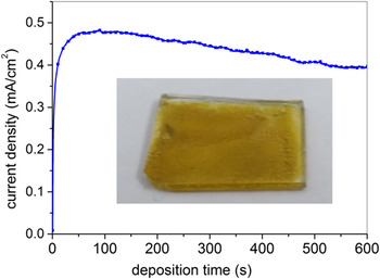
Figure 1 shows the chronoamperometric curve plotted against deposition time. A rapid increase of current density is observed at 0–80 s, then the current density decreases gradually over 100 s as the deposition time is passing. It is suggested that the process at 0–80 s is due to capacitive current, while the process over 100 s is due to diffusion current. In inset of Fig. 1 is shown a picture of the IrQ(ppy)2 ED film which was deposited on ITO/glass substrate for 30 min. A yellow-brown color film is observed. The film thickness is about 1 μm.
Electrodeposition IrQ(ppy)2 thin film.

B. Morphology
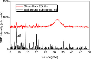
The XRD pattern of 50 nm thin film consists of continuous curve with a broad band at 2θ = 32° and several very weak discrete lines (Fig. 2). This film was obtained by ED time of 4 min. It seems that the continuous part reflects noncrystalline amorphous phase. After subtraction of the background due to amorphous phase, we obtained a pattern consisted of sharp lines as shown at the bottom of Fig. 2.
X-ray diffraction patterns of ED film with 50 nm thickness.

These sharp lines seems to reflect the crystalline phase which is related with the rectangular products observed in the SEM image. To check the origin of the sharp lines of XRD, we examine the SEM image and XRD of another ED film which is much thicker than 50 nm.
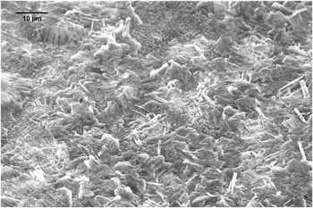
The SEM image is shown for a IrQ(ppy)2 ED film with thickness of 50 nm in Fig. 3. The SEM image indicates the amorphous phase in the whole area. From careful examination of the image, we found several small slender rectangle products with micro-size, which are immersed in the amorphous phase. These minor products suggest presence of micro-crystals.
SEM image of ED film with 50 nm thickness.

Formation of amorphous phase has been reported for the organic compounds electrochemically deposited on ITO, for compound peripheral carbazole substituted 9,9′-spirobifluorene (TCPC) by Gu et al. Reference Li, Tang, Shen, Liu, Wang, Lu, Hanif and Ma10–Reference Gu, Tang, Yang, Liu, Wang, Yang, Hanif, Lu, Shen and Ma13 and for polybithiophene (PBTh) by Wang et al. Reference Wang, Wong and Hu2
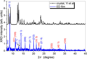
The XRD of the 1 μm thick ED film is shown at the bottom of Fig. 4. The pattern is the same as the XRD pattern shown at the bottom of Fig. 2, which was obtained from the 50 nm thick ED film. This indicates that the small rectangle-like products observed in the 50 nm thick film were grown to the parallelogram-shape products by increase of the deposition time from 4 min to 30 min.
X-ray diffraction patterns of ED film with 1 µm thickness.

By the analysis of the XRD pattern obtained from the 1 μm thick ED film using the Crystal Sleuth software, we obtained coexistence of two kinds of monoclinic structures, i.e., (i) the peaks at 2θ (°) = 8.8, 12.7, 13.0, 13.9, 15.9, 18.1, 20.0, and 23.6 are related with the (
 ${\rm{10}}\bar 1$
), (
 $11\bar 1$
), (111), (
 $10\bar 3$
), (200), (
 $21\bar 1$
), (212), and (
 $21\bar 4$
) lattice planes, respectively, [the (hkl) lattice plane indices indicated by blue letters in Fig. 4] of a monoclinic structure (space group P21/n) with crystal parameters of a = 10.85 A, b = 9.13 A, c = 21.79 A, α = 90°, β = 92°, and γ = 90°, and (ii) the peaks at 2θ (°) = 11.1, 11.3, 21.3, 22.5, 29.5, 32.6, and 35.4 are related with the (021), (120), (
 $10\bar 3$
), (050), (232), (
 $42\bar 1$
), and (124) planes [the (hkl) indices indicated by red letters in Fig. 4] to another monoclinic structure (space group P21/n) with a = 11.5 A, b = 19.72 A, c = 12.59 A, α = 90°, β = 110°, and γ = 90°. It is suggested that the latter and former monoclinic structures with β = 110° and 92° correspond to the parallelogram- and triangle-like products observed from the SEM images respectively.
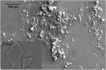
Figure 5 shows the SEM image for a 1 μm thick IrQ(ppy)2 ED film. This film was obtained by ED time of 60 min. Unlike the case of the 50 nm thick film, the SEM image clearly shows the presence of many randomly distributed crystal-like products. Some products show parallelogram- and rectangle-like shapes. Most products; however, are fragments with various shapes. It seems that the fragments have not completed the crystallization into single crystal. Many products are poly-crystalline states which consist of several domains of single crystals randomly oriented.
SEM and BSE (inlet) images of ED film with 1 µm thickness.

To find single-crystal-like products, we examined the BSE image in a small area of the 1 μm thick ED film. They are shown in Fig. 5 inlet. A parallelogram-like product with angles of about 108° and 72° is observed, together with a triangle-like product with an angle of about 92°. This 92° is close to β = 93° in the monoclinic structure obtained by Yi et al. Reference Yi, Yang, Liu, Xu, Wang, Cao and Gao24 and Kappaun et al. Reference Kappaun, Eder, Sax, Mereiter and Slugovc25 The BES and SEM images suggest appearance of two kinds of monoclinic structures.
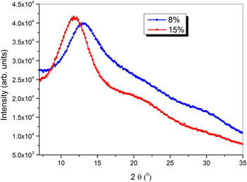
Orientation of emitting dipoles in organic light-emitting diodes (OLEDs) due to the crystallization behaviors as a result of close packing process induces a strong coupling efficiency. Using grazing incidence X-ray diffraction (GIXRD), we find that the emitter form crystallite grains that are pertained even when the emitter is doped into a host. Figure 6 shows the grazing incident X-ray diffraction in the case of 8% wt and 15% wt doped CBP films.
Grazing incidence X-ray diffraction measurements on IrQ(ppy)2:CBP films.

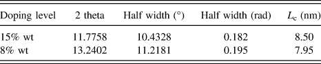
The Bragg reflections at 11.8° and 13.2° show the variation of the crystalline grains of IrQ(ppy)2 with the concentration of the emitter molecules in CBP. To quantify the grain size, we fitted the GIXRD spectra with Gaussian functions to extract the exact position and FWHM of the Bragg reflection. From the peak position 2θ and the FWHM, the coherence length L c can be calculated via the Scherrer equation Reference Rivnay, Mannsfeld, Miller, Salleo and Toney26 :
 $${L_{\rm{c}}} = {{K\lambda } \over {\cos \left( {{{2\theta } \over 2}} \right){\rm{FWHM}}}}\quad ,$$
where K denotes a shape factor that is set to 1, while λ is the wave length of the X-rays. The resulting L c and 2θ are summarized in Table I.
Fitting parameters of Bragg reflections as obtained from GIXRD spectra of IrQ(ppy)2.

The coherence length significantly decreases when doping level increases. In these investigations, the coherence length denotes the minimum size of an aggregate in out-of-plane direction (i.e., perpendicular to the substrate). Hence, aggregates may be much larger if the concentration of dopant is higher.
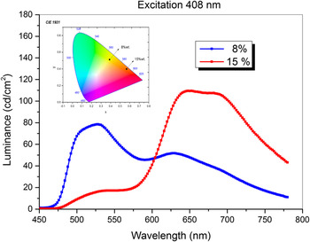
The crystallization behaviors can be seen in the luminance spectra which gives a direct measure of the internal quantum efficiency of the two concentrations in CBP. Depending on doping level the luminance is balanced between red and green emission (Fig. 7). CIE measurements suggest a shift of the all over emission color from yellow to red with the concentration going from 8% wt to 15% wt.
Luminance and CIE measurements on IrQ(ppy)2:CBP films.

For the IrQ(ppy)2 organometallic compound, the stacking distances between quinoline ligands compete with the intermolecular interactions Reference Ding, Gao, Fu, Cheng, Ma and Wang27 and induces inter-ligand energy transfer (ILET). Reference You and Park28 After excitation in the 1MLCT state, an efficient inter-system crossing to the 3MLCT occurs due to the strong spin–orbit coupling.
The experimental measurements of the IrQ(ppy)2 photoluminescence versus stacking in the CBP matrix show drastically decreasing red emission resulting from destruction of the crystalline structure. It can be clearly observed that the emission changes from red to green colors are controlled by the quinoline ancillary ligand. This observation is confirmed by other iridium based organometallic compounds with ancillary ligands, such as 1-isoquinolinate and 3-isoquinolinate. Reference Holmes, Forrest, Tung, Kwong, Brown, Garon and Thompson29 When the concentration of IrQ(ppy)2 molecules increases in CBP film, the crystallization phenomena can be observed due to the reduction of the distances. In this case the orientation of the quinoline ligands lead to intermolecular transfer across the π–π stacking between molecules. According to the Forester energy transfer model, the transfer rate is increased with decreasing of the distances between neighboring molecules. Reference Dale, Eisinger and Blumberg30,Reference Mersol, Wang, Gafni and Steel31
The stacking of the IrQ(ppy)2 in CBP can also influence the electroluminescent behaviors of the organometallic compound. This situation is similar to IrQ(ppy)2-5Cl stacked in a CBP conducting polymer, which exhibits higher red electroluminescence than the green electroluminescence. Reference Pommerehne, Vestweber, Guss, Mahrt, Bassler, Proseh and Daub32
IV. CONCLUSIONS
Neat films of IrQ(ppy)2 were directly obtained by ED on ITO/glass substrates. The electrodeposition potential was set at 0.66 V where the first quasireversible oxidative wave with anodic peaks is observed, which was assigned to the oxidation of the Ir metal center [Ir3+/Ir4+]. The deposition time changes the thickness for the ED film which influences the morphology of their surfaces and the emission properties of the ED film. It was found from the SEM and BSE images and the XRD pattern that (i) amorphous phase is predominantly formed in thin IrQ(ppy)2 ED film with thickness of 50 nm although very small amount of crystalline products are formed, and (ii) the crystalline phase is grown and many micro-crystals are randomly distributed in the IrQ(ppy)2 ED film by the increase of the film thickness. The crystalline phase consists of two kinds of monoclinic structures with different β angles, one is β = 92 and the other is β = 110°.
Like the cases of IrQ(ppy)2 in solution and spin-coated film, dual emission of green and red emission bands is observed in the IrQ(ppy)2 ED films too. The red emission intensity relative to the green emission intensity is found to change by the thickness of ED film. Higher green emission intensity than the red emission is observed in the thin ED film with thickness of 50 nm, while the reverse is observed in the thick film of 1 μm as the case of IrQ(ppy)2 powder. This is understood by the coexistence of the amorphous phase and the crystalline phase in the ED film, i.e., minor micro-crystal products are present in the amorphous phase in the thin film, while the many micro-crystals are randomly distributed in the thick ED film.
For doped conducting thin films, the level of doping induces the aggregation processes of the IrQ(ppy)2 organometallic compounds, in which the orientation of the quinoline ligands lead to intermolecular transfer across the π–π stacking between molecules. Modifications in the coherence length with the doping level indicates the formation of the crystalline phase with π–π stacking between molecules which influences the energy transfer between molecules and change the luminance properties of the active layer and the internal quantum efficiency.
ACKNOWLEDGMENTS
This work was supported by a grant of the Romanian National Authority for Scientific Research, CNCS-UEFISCDI, Project number PN-II-ID-PCE-2011-3-0620 and Core Program of NIMP PN16-480103.