I. INTRODUCTION
The electrodeposition for preparation of thermoelectric films has gained a lot of interest because of its simplicity, scalability, low cost, and high growth rate.Reference Boulanger1 Therefore, characterization for thermoelectric properties of electroplated films is important. Seebeck coefficient is determined from the voltage ΔV generated between two points over which a temperature difference ΔT is maintained

This principle works well for bulk samples or films prepared on nonconductive substrates (such as by evaporation or sputtering). However, electroplated films always consist of a conductive seed layer, which may cause short circuit effect during measurement of Seebeck coefficient. Therefore, direct application of this method for electroplated films will lead to incorrect results.
This challenge has been recognized and treated elsewhere in literature.Reference Lim, Kim and Oh2–Reference Li and Wang7 Based on the sense that if the seed layer is resistive enough, its effect on the measurement result may be negligible, Lim et al.Reference Lim, Kim and Oh2 used the poor conductivity metal (1 μm of Ti) as the seed layer to prepare bismuth (antimony) telluride testing samples. Although Yoo et al.Reference Yoo, Huangb, Limb, Hermanb, Ryanb, Fleurial and Myung3 used sputtered bismuth telluride seed layers for electrodepositing bismuth telluride films, they believed the seed layer and the film had the same Seebeck coefficient. Even though the approaches seemed logical, there was no quantitative evaluation for the effect of the seed layer on the measured Seebeck coefficient. Miyazaki and KajitaniReference Miyazaki and Kajitani4 removed the electroplated films from the seed layer before measuring the Seebeck coefficient to eliminate the seed layer’s effect. Other authors transferred the deposited films to new nonconductive substrates.Reference Takahashi, Kojima, Ohnisi, Nishiwaki, Wakita, Miyuki, Ikeda and Muramatsu5–Reference Li and Wang7 Although this approach completely eliminates the effect of the seed layer, the transfer may introduce stress and cracks into the films, which possibly change the films’ properties.Reference Boulanger1
In this work, the effect of the seed layer on in-plane Seebeck coefficient measurement of electroplated films is quantitatively studied and validated by finite element simulation and experiments. Based on the results, methods to minimize the effect of a seed layer are discussed and a new method to determine Seebeck coefficient of electroplated films is suggested and examined.
II. THEORETICAL CONSIDERATION
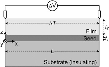
The setup to measure in-plane Seebeck coefficient of an electroplated film in presence of a seed layer is shown schematically in Fig. 1 where, for clarity, the dimensions in the thickness direction are exaggerated compared to the length of the specimen. We assume the material properties are isotropic and temperature independent because measurements are usually carried out over a narrow temperature range. On the other hand, since the thickness of the film and the seed layer are much smaller than their width and length, temperature can be considered uniform over the width and the thickness of the sample (y- and z-directions in Fig. 1). As a result, no heat exchanges through the interface. If the charge exchanged through the seed–film interface is negligible, the film and the seed layer can be treated as two individual thermoelectric elements. The equations that govern the steady-state transport of heat and charge for each layer in the system are given by


Schematic of a setup for measuring Seebeck coefficient of electroplated films. For clarity, the vertical dimensions are grossly enlarged compared to the length of the specimen.

together with the constitutive thermoelectric equationsReference Landau and Lifshitz8


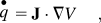
where
T = absolute temperature, K;
V = electric potential, V;
 = heat production rate per unit volume, W/m3;
q = heat flux vector, W/m2;
J = electric current density vector, A/m2;
λ = thermal conductivity, W/(m·K);
σ = electrical conductivity, 1/(Ωm);
α = Seebeck coefficient, V/K.
Considering the film, because temperature is uniform over the y- and z-axes, the problem becomes 1-D, and the divergences of temperature and electrical potential in Eqs. (4)–(6) can be replaced by gradients  and
 , respectively. Substituting Eq. (4) into Eq. (6) with notation of Eq. (3) yields
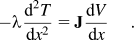
When the seed layer is very resistive, the net current J in Eq. (5) is close to zero, and hence,  can be approximated to zero. The temperature gradient is, thus, a constant,
 where L is the length of the sample (see Fig. 1). As a result, the potential gradient is also a constant,
 The current flowing in the film can be obtained from Eq. (5)
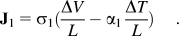
Likewise, the same derivation yields the current flowing in the seed layer
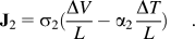
Application of Kirchhoff’s law at one end of the sample yields

where t denotes thickness and w the width of the sample (w 1 = w 2), subscripts 1 and 2 denote the seed layer and the film, respectively. By rearranging this equation and noting sheet resistance as R □ = 1/σt, the Seebeck coefficient of the seed–film system α measured by the setup is given by

III. SIMULATION AND EXPERIMENTAL VALIDATION
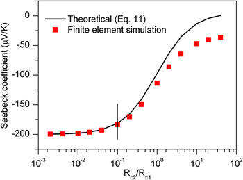
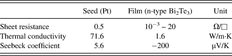
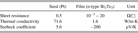
The validity of Eq. (11) was examined by comparing it to finite element calculation using COMSOL. A seed–film system was simulated with material properties of a Bi2Te3 film on a Pt seed layer, as summarized in Table I. Seebeck coefficients of the seed–film system predicted by Eq. (11) and those calculated by COMSOL are compared in Fig. 2. The Seebeck coefficients overlap at low sheet resistance ratios R □2/R □1 because Eq. (11) is derived based on the assumption that the current in the system is small, i.e., when the seed layer is very resistive. Figure 2 shows that if an accuracy of 1% is considered, a ratio R □2/R □1 of 0.1 can be taken as the application limit of Eq. (11).
Seebeck coefficients of Bi2Te3 / Pt films by finite element simulation as a function of the sheet resistance ratio R□2/R□1 compared to the theoretical calculation using Eq. (11). Up to R□2/R□1 = 0.1, the deviation is less than 1% (left side of the bar).

Materials properties used in finite element simulation.
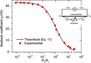
To experimentally examine the calculation, an “imaginary” seed–film system was subjected to Seebeck coefficient measurements illustrated in the inset in Fig. 3. In the experiments, a constantan wire (which acts as the “film”) and a copper wire (acting as the “seed layer”) were fused together at both ends. The resistance of the “seed layer” was changed by inserting different resistors in series with the copper wire. Figure 3 shows the Seebeck coefficient of this modified T-type thermocouple as a function of the resistance ratio between the resistor and the constantan wire in comparison to the prediction by Eq. (11). The agreement between Eq. (11) and the experiments holds up to a ratio R □2/R □1 of 2. This higher limit compared to the case of simulation can be understood because the “film” and the “seed layer” were not in contact, which perfectly satisfied the assumption that heat and charge did not exchange through the interface.
Seebeck coefficients of a modified type-T thermocouple in comparison with theoretical calculation using Eq. (11). Resistance ratio is changed by varying the parallel resistors (see inset).

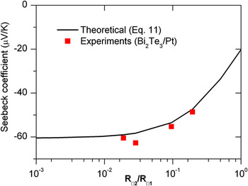
Next, the analysis is examined on real seed–film systems, which are bismuth telluride films on Pt (10 nm)/Ti (10 nm) seed layers on SiO2 (500 nm)/Si substrates. The films were electroplated from a bath containing 1 M HNO3, 0.02 M TeO2, and 0.0075 M Bi2O3 at 50 °C by applying constant current density of 3 A/dm2. To obtain different sheet resistances, the films were prepared up to different thicknesses by varying deposition time, 10, 20, 60, and 75 min, respectively. The sheet resistances were directly measured by the 4-point method without determining film thickness. Measurements on the seed layers indicate its Seebeck coefficient α 1 = +20.1 μV/K. As shown in Fig. 4, the measured Seebeck coefficient decreases, following the trend predicted by Eq. (11) when the sheet resistance ratio increases (thinner film). Here, Seebeck coefficient of the thickest film, −61.5 μV/K, was used for α 2 in Eq. (11) as the real Seebeck coefficient of the bismuth telluride material. It can be observed from the figure that all the experimental data points distribute only on one side of the theoretical prediction (higher absolute values). This is because the Seebeck coefficient of the thickest film used as α 2 in Eq. (11) for the theoretical calculation is experimentally measured in presence of a seed layer; it is certainly smaller than the real Seebeck coefficient of the deposited material.
Seebeck coefficients of bismuth telluride films electroplated on Pt/Ti seed layers in comparison with theoretical calculation using Eq. (11). The films are grown from a bath containing 1 M HNO3, 0.02 M TeO2, 0.0075 M Bi2O3, at 50°C by applying constant current density of 3 A/dm2 in different deposition time 10, 20, 60, and 75 min.

IV. DISCUSSION
Equation (11) implies that, in presence of a seed layer, the conventional measurement [as in Fig. 1 and using Eq. (1)] does not give the Seebeck coefficient of the thermoelectric film, but an average Seebeck coefficient of the film and the seed layer, weighted by their sheet resistances. The effect of the seed layer (relative error of the experiment) can be quantitatively estimated
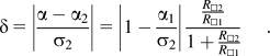
To reduce this effect, one may choose a seed layer that has similar Seebeck coefficient to the deposited film. In this case, the first factor in Eq. (12) will be close to zero, and so will δ. Although this approach has been utilized in the work by Yoo et al.,Reference Yoo, Huangb, Limb, Hermanb, Ryanb, Fleurial and Myung3 in which a bismuth telluride seed layer was used to prepare bismuth telluride films, it is not practically relevant. First, most of thermoelectric materials are alloys, whose Seebeck coefficient usually varies in a wide range, even changes from negative to positive or vice versa depending on the alloy composition. This makes the error uncertain and possibly very large. Second, materials with high Seebeck coefficient usually have higher electrical resistivity. Thus, a thick layer is required to provide sufficient conductance for electrodeposition, which makes the preparation of such seed layers costly and time consuming.
If low Seebeck coefficient materials, such as metals, are used for a seed layer, the first factor in Eq. (12) is limited to 1 because Seebeck coefficients of metals are usually much smaller than those of thermoelectric films. The second factor can be minimized by reducing the sheet resistance ratio, which in turn can be reduced by either lowering sheet resistance of the film or raising the sheet resistance of the seed layer. By choosing Ti, a high resistivity material, as seed layer for the electrodeposition of bismuth antimony telluride films, Lim et al.Reference Lim, Kim and Oh2 has applied the former approach. However, in this work, the authors failed to determine correct Seebeck coefficient of the deposited films. The sheet resistance ratio, estimated for 1-μm-Ti seed layers and 2-μm-bismuth antimony films, was about 47 (ρ 1 = 0.42 μΩm, ρ 2 = 40 μΩm, t 1 = 1 μm, t 2 = 2 μm2), giving the relative error of more than 97%, which is not negligible.
Thus, the requirements to determine the real Seebeck coefficient of an electroplated film in presence of a seed layer are (i) the seed layer should be prepared from low Seebeck coefficient materials and (ii) the sheet resistance ratio between the film and the seed layer R □2/R □1 should be small. If an accuracy of 99% is desired, a ratio of 0.01 or lower is required for the sheet resistance ratio. This condition requires very thin seed layers and/or very thick films. For example, if a seed layer of 10 nm Pt (ρ 1 = 0.1 μΩm) is used for electrodeposition of bismuth telluride films (ρ 2 = 10 μΩm9), the film thickness t 2 should be more than 100 μm, which is not practically relevant.
However, Seebeck coefficient of the film can be estimated from Eq. (11) as
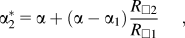
where Seebeck coefficients of the seed layer α 1 and of the seed–film system α can be measured with the setup in Fig. 1 and the sheet resistances can be determined, e.g., by 4-point measurement. Applicability of this method depends on the validity of Eq. (13), or actually Eq. (11), which in turn is determined by the sheet resistance ratio R □2/R □1. As seen in Fig. 5, where this method was applied to the data of Section 3, the correct Seebeck coefficients can be estimated up to a sheet resistance ratio R □2/R □1 of at least 0.1. This limit is 10 times higher than 0.01 in case of neglecting the seed layer’s effect, which means the film thickness required for measurement is reduced with a factor of 10 (about 10 μm for the Bi2Te3 films on the 10 μm Pt seed layer in the example discussed above).
Corrected Seebeck coefficient α2* evaluated by Eq. (13) for the simulated Bi2Te3 / Pt films, the type-T thermocouple, and the electrodeposited Bi2Te3 / Pt films as functions of sheet resistance ratios R□2/R□1.

Application of Eq. (11) can explain the contradictory experiment result by Takahashi et al.Reference Takahashi, Kojima, Ohnisi, Nishiwaki, Wakita, Miyuki, Ikeda and Muramatsu5 that negative Seebeck coefficient was observed for bismuth telluride films, whereas p-type behavior was confirmed by Hall effect measurement. In that experiment, a p-type bismuth telluride film was transferred to resin (nonconductive) substrates before Seebeck coefficient measurements to eliminate the effect of the original seed layer. However, the depth profile showed a Te-rich layer near the seed layer, whose conductivity was determined of 100 times larger than that of the p-type layer. Because thicknesses of those two layers were similar, their sheet resistance ratio R □n/R □p was about 0.01. As a result, the authors observed 99% property of the n-type layer in Seebeck coefficient measurement.
The failure of the analytical model [Eq. (11)] to describe seed–film systems in Seebeck coefficient measurement at high sheet resistance ratio (R □2/R □1 > 0.1) can be explained by the dissatisfaction of the central assumption that no electric current flows through the seed–film interface (except at two ends). To understand this phenomenon, it should be noticed that charge carriers in a thermoelectric element subjected to a temperature gradient are driven by both temperature and potential gradient, creating j Q and j E, respectively. In equilibrium, these two currents compensate and the net current flowing in the element is zero. This is the case for a thermoelectric film on a resistive seed layer where j E (of the film) flows within the film. However, charge carriers of the film prefer flowing in the seed layer when the seed layer is more conductive than the film, forming an electric current through the interface. The higher sheet resistance ratio, the higher this current, and as a result, the less valid is the calculation [Eq. (11)] as previously observed in the validation results.
V. CONCLUSION
Quantitative analysis has been performed for Seebeck coefficient measurements of electroplated thermoelectric films in presence of a seed layer (seed–film systems). It is found that the measurement result is the weighted average of Seebeck coefficients of the film and the seed layer. The contribution of the film and the seed layer to the measured result is determined by their sheet resistance, rather than bulk resistance. Finite element simulation and experiments verified that the analysis is valid as long as the ratio of sheet resistances of the film and the seed layer is smaller than 0.1. The analysis is applicable for Seebeck coefficient measurement of any two-layer system.
Based on the analysis, approaches to minimize the seed layer’s effect have been discussed and related to cases in literature. According to that, to neglect the effect of the seed layer, low Seebeck coefficient materials should be used and the ratio between sheet resistance of the film and the seed layer should be smaller than 0.01. The latter condition requires very thin seed layer and/or very thick films. This condition contradicts with the vital requirement in electrodeposition that the seed layer must be highly conductive. We proposed and examined a more practically relevant method, in which the required sheet resistance ratio is reduced by a factor of 10, i.e., thicker seed layers and thinner films can be characterized. This approach for determining Seebeck coefficient is simple, and more importantly, electroplated films can be characterized in their statu nascendi.
ACKNOWLEDGMENT
The authors acknowledge the Holst center (The Netherlands) for financial support.