Introduction
Semiconductor to metal contact engineering and contact material development have become crucial in recent years to keep pace with the continual improvement in electronic device performance. As device dimensions shrink and device performance improves, increasing current densities in devices is causing the semiconductor-metal contacts and semiconductor junctions to severely affect the device performance. This will require new contact materials and innovative materials engineering to cater to complementary metal-oxide semiconductors (CMOS) in dual n-type and p-type contacts requirements. In addition, introduction of new device architectures such as FinFET (fin-shaped field-effect transistor) and nanowire FETs is also accompanied by technological challenges in contacts, such as requirements for three-dimensional contact schemes.
This review focuses on some of the key issues in the development of contact materials for advanced Si CMOS technologies. Various ways to engineer highly conductive silicide contacts (see Figure 1 in the article by Wen and Chambers in this issue) for a sub-32 nm technology node will be explored. Techniques of lowering Schottky barrier height (SBH) in nickel silicide by usage of low work function metals, improved carrier concentration via dopant segregation, implanted impurity, and silicide phase modulation will be discussed, with particular focus on the technology requirement of contact pitch scaling for a sub-32 nm technology node.
Silicide contacts
Ohmic contacts to semiconductors have typically been achieved through a single metal or silicide to degenerately doped silicon. For sub-50 nm gate length, the contribution of the contact resistance R co (or contact resistivity ρCO when normalized by area), which is the resistive component from the metal silicide to the highly doped source drain, is expected to dominate over other parasitic components.Reference Kim, Park and Woo1 Yu proposed a theoretical model for thermionic field emission between the metal/silicide and silicon, which shows ρCO is directly proportional to the SBH, ϕB, and is inversely proportional to the square root of the dopant concentration, N d, in the semiconductor.Reference Yu2 See Equation 1 in the introductory article of this issue.
Work function modulation
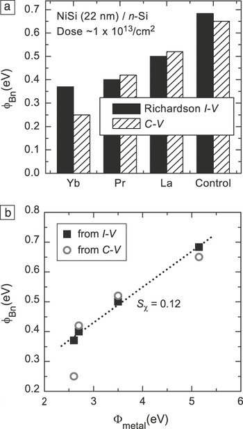
While NiSi has a low Schottky barrier to p-Si(100), ϕBp, it has a complementary high Schottky barrier, ϕBn, of 0.65–0.7 eV on n-Si(100), since ϕBn + ϕBp = 1.1 eV (Si bandgap). Using rare-earth metals (which have one of the lowest metal work functions), Tu et al. have shown a low ϕBn of 0.37–0.39 eV for disilicides of Dy, Er, Gd, Ho, and Y to n-Si.Reference Tu, Thompson and Tsaur3 Further studies also have shown that a very high hole Schottky barrier ϕBp of 0.82 eV (corresponding to ϕBn ~0.27 eV assuming ϕBn = E g – ϕBp) can be obtained with YbSi2.Reference Zhu, Chen, Li, Lee, Singh, Zhu, Du, Tung, Chin and Kwong4 Instead of adopting the dual silicide (for n- and p-type contact) approach, an alternative is to use a single silicide but to incorporate the rare-earth impurities into the NiSi/Si interface. Figure 1a shows the measured ϕBn of nickel silicide with different metal implanted into n-Si prior to the nickel silicidation (the “pre-silicide” state). The rare-earth metal is implanted into the n-Si prior to the nickel deposition at a similar dose of 1 × 10¹³/cm2 but with a slightly different energy to achieve the same projected range (to cater to the difference in rare-earth metal atomic mass). Secondary ion mass spectroscopy depth profile of the subsequent nickel silicide shows segregation of the rare-earth at the NiSi/Si interface, which is similar in behavior to dopant segregation in nickel silicide.Reference Kinoshita, Tanaka, Uchida and Koga8, Reference Zhang, Knoch, Zhao, Breuer and Mantl9
According to Mott-Schottky theory,Reference Schottky10, Reference Mott11 the SBH, ϕB, between a metal/silicide with a work function of ΦM and a semiconductor with electron affinity χ is given by

(a) Schottky barrier height (SBH) of NiSi on n-Si with various pre-silicide implants (implant fluence of 1 × 10¹³/cm2). SBH, ϕBn is measured using a Richardson plot of reverse leakage currentReference Chino6 at 0.5 V and depletion capacitance-voltage (C-V) measurementsReference Chino6, Reference Sze7 at 100 kHz. A significant discrepancy is observed in the ϕBn measurement from Richardson plot and depletion C-V for Yb, and this is attributed to frequency-dependent traps response during the C-V measurement. Reprinted with permission from Reference 5. © 2010, American Institute of Physics, (b) Measured SBH for NiSi on n-Si with various pre-silicide metal impurities versus the metal work function. A less than unity interface index Sχ, as defined in Equation 2, shows an imperfect interface with a high degree of Fermi-level pinning.

Equation 1 suggests a unity slope between ϕB and metal/silicide work function ΦM, with  . In reality, most experimental results show various degrees of Fermi-level pinning, with a less than unity interface index Sχ defined as

Low values of Sχ are observed, especially in covalent semiconductors (e.g., Si and Ge). Figure 1b shows the correlation between the measured ϕBn and the work function of the rare-earth metal and control samples with Ni. A linear correlation between the measured ϕBn and metal work function is observed, although the slope S χ = 0.12 is much lower than unity. This agrees with the Fermi-level pinning effects observed in the studies by TungReference Tung12 and Kurtin,Reference Kurtin, McGill and Mead13 which show a low S χ of between 0.1 to 0.2 for silicon. The effective modulation of ϕB in implanted rare-earth impurities NiSi shows that pre-silicide ion-implantation can be a viable alternative to dual metal silicides.
Interfacial dielectric dipole engineering
The low interface index S χ for Si suggests that interface properties rather than bulk properties such as metal work function govern the actual ϕB. Two main theories explaining the mechanism have been proposed: (1) Dipole formation due to bond polarization at the metal-semiconductor interface and (2) metal-induced gap states (MIGS), which explain Fermi-level pinning in a metal-semiconductor coupling as the extension of the metal wave function into the semiconductor. The MIGS theory assumes that the metal/silicide induces the gap states, but the actual density of the gap states is dependent on the semiconductor.Reference Tejedor, Flores and Louis14, Reference Tung15 According to the MIGS theory, passivating the gap states of the underlying semiconductor will relieve the Fermi-level pinning effect, and hence recover the unity relation between ϕB and the metal work function.
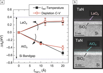
Several groups have reported great success in relieving the Fermi-level pinning effect by the insertion of an ultrathin dielectric into various semiconductors. Connelly et al. showed Mg and Yb contacts to n-Si with interfacial silicon nitride that demonstrate a low barrier height of 0.2 eV.Reference Connelly, Faulkner, Grupp and Harris16 Similiarly, Takahashi et al.Reference Takahashi, Nishimura, Chen, Sakata, Kita and Toriumi17 and Kobayashi et al.Reference Kobayashi, Kinoshita, Saraswat, Wong and Nishi18 both separately demonstrated good device performance on a Ge substrate using metal-to-Ge with an interfacial GeOx or SiN layer, respectively. An alternative approach is to use an interfacial layer that both passivates and incorporates dipoles to help modulate the final ϕB.Reference Coss, Loh, Oh, Smith, Smith, Adhikari, Sassman, Parthasarathy, Barnett, Majhi, Wallace, Kim and Jammy19,Reference Coss, Loh, Wallace, Kim, Majhi and Jammy20 Figure 2 shows the near band-edge SBH using TaN with AlOx/SiO2 or LaOx/SiO2 interfacial dipoles. The LaOx and AlOx dielectrics are deposited onto a clean n-Si, and interfacial SiO2 is formed naturally during the annealing cycle due to the difference in electronegativity and oxygen affinity. The inclusion of about 1 nm of high-κ dielectrics is able to both passivate and modulate the ϕBn of TaN on n-Si by more than 0.2 eV, achieving close to band edge modulation with 2 nm of dielectrics. The observed ϕB shifts correspond closely to the reported dipole moment for AlOx/SiO2 and LaOx/SiO2 interfaces.Reference Kita and Toriumi21 While higher dielectric thickness incorporates higher amounts of dipoles, tunneling probability is also reduced due to the enhanced thickness, and hence optimization of the process is required for contact application. Due to the conformal deposition of high-κ dielectrics or SiN, this contact scheme can ideally be implemented in any two- or three-dimensional contact structure.
(a) Schottky barrier height (SBH [ϕB]) tuning as a function of AlOx and LaOx, high-κ thickness on p-Si calculated with respect to TaN/p-Si control. Nearly band-edge SBHs are obtained using LaOx and AlOx on p-Si. (b) A transmission electron microscopy image of 10 nm of LaOx and AlOx capped with TaN metal on a n+Si substrate. Reprinted with permission from Reference 20. © 2009, American Institute of Physics.

Phase modulation of nickel silicides
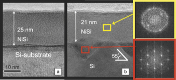
Nickel is known to form three different phases of silicide (Ni2Si, NiSi, and NiSi2), depending on the annealing temperature.Reference Lauwers, Steegen, de Potter, Lindsay, Satta, Bender and Maex22, Reference d’Heurle, Peterson, Baglin, La Placa and Wong23 At temperatures <350°C, Ni-rich Ni2Si is formed with intermediate resistivity and high ϕBn, while at temperatures >750°C, a Si-rich NiSi2 phase is formed with ϕBn ranging from 0.4 eV to 0.65 eV,Reference d’Heurle, Peterson, Baglin, La Placa and Wong23, Reference Fujitani24 but with significantly higher resistivity. Using nitrogen implantation, a phase-modulated Ni silicide has been demonstrated for CMOS integration at the same silicidation temperature.Reference Loh, Hung, Coss, Kalra, Ok, Smith, Kang, Lee, Oh, Sassman, Majhi, Kirsch, Tseng and Jammy25 Figure 3 shows the cross-sectional transmission electron microscopy images of the control NiSi (unimplanted sample) and samples on Si(100) with a high dose (3.5 × 10¹⁵/cm2) of N implanted before Ni deposition. The resistivity of the N-implanted NiSi is higher than NiSi but significantly lower than NiSi2. In addition, implanted samples also show pyramidal silicide at the {111} facet, which is attributable to preferential NiSi2 formation along the Si(111) plane, although these facets are sparse.
High-resolution transmission electron microscopy micrograph of (a) control NiSi without a N-implant and (b) with a N-implant (3.5 × 10¹⁵ N/cm2). NiSi with a N-implant shows a thinner silicide with facets observed at the Si(111) interface. The scale is the same for (a) and (b). Fast Fourier transforms (FFTs) (right) on bulk Ni silicide and on the interfacial facets for samples with N-implant are also shown. FFTs on interfacial facets show fcc structures, epitaxial to the underlying Si substrate.

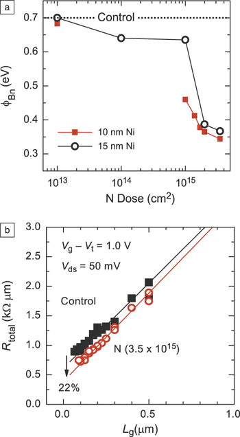
The electrical characteristics of N-implanted NiSi also have been studied. Figure 4a shows the Schottky barrier extracted from a Richardson plot using the reverse leakage for both control NiSi (without pre-silicide implant) and N-pre-silicide implanted samples, with temperatures ranging from 300 K to 400 K. For the N-implanted dose of > 1 × 10¹⁵/cm2, the Schottky barrier, ϕBn, reduces from the control of 0.7 eV to about 0.34 eV. The large reduction in ϕBn is consistent with reported Schottky barriers for NiSi2.Reference Tung, Levi, Sullivan and Schrey26 A source/drain dopant segregated n-channel MOSFET with N-pre-silicide implanted NiSi has been fabricated and characterized.Reference Loh, Hung, Coss, Kalra, Ok, Smith, Kang, Lee, Oh, Sassman, Majhi, Kirsch, Tseng and Jammy25 Figure 4b shows the extracted total resistance from drive current at overdrive of gate voltage, V g – V t = 1.0 V (where Vt is the threshold voltage) as a function of different gate length, L g. Series resistance R ext for N-implanted samples shows a 22% reduction, due mainly to R co reduction.
(a) Summary of electron ϕBn for various doses of N-implant. At high dose, N-implanted samples show ϕBn close to typical values for NiSi2. Solid symbols reflect data for thin 10 nm Ni, while open symbols show data for thicker Ni silicide with 15 nm of deposited Ni. (b) Total device resistance (R total) as a function of printed gate length, L g, in dopant-segregated source/drain (DSS) n-channel MOSFETs. Control samples without nitrogen implant are shown as solid symbols, while open symbols reflect data for N-implanted samples. N-implanted DSS-nFETs show a 22% reduction in R total compared to control due to a reduction in R co.

Summary for silicide contacts
This article discusses the various schemes for modulating the Schottky barrier height ϕB to reduce contact resistivity. Significant progress in tuning the ϕB has been achieved using low work function metals such as YbSi2 (ϕBn < 0.3 eV)4 or by pre-silicide ion-implantation and segregation (ϕBn < 0.4 eV). To relieve the Fermi-level pinning observed mainly in Si and Ge with covalent bonds, interfacial layer engineering has reduced ϕBn of metal-to-n-Si to 0.2 eV.Reference Connelly, Faulkner, Grupp and Harris16 Complementary metal oxide semiconductor compatible dielectric dipole mitigated contacts have also been demonstrated, which could reduce ϕB to both n-Si and p-Si by insertion of LaOx or AlOx, respectively.Reference Coss, Loh, Oh, Smith, Smith, Adhikari, Sassman, Parthasarathy, Barnett, Majhi, Wallace, Kim and Jammy19,Reference Coss, Loh, Wallace, Kim, Majhi and Jammy20 Finally, phase modulation of NiSi is observed when nitrogen is implanted prior to silicidation. Nitrogen acts as a Ni diffusion barrier and enhances NiSi2 interfacial formation, which reduces ϕBn from nominal values of 0.7 eV to 0.34eV.Reference Loh, Hung, Coss, Kalra, Ok, Smith, Kang, Lee, Oh, Sassman, Majhi, Kirsch, Tseng and Jammy25 The various schemes show substantial ϕBn modulation down to 0.3 eV, which is critical for achieving sub 10−8 Ωcm2 contact resistivity for the sub-32 nm technology node.