Introduction
Due to the emergence of microwave and millimeter-wave communication, high gain and wideband electronically beam scanning antenna are in high demand. Achieving high antenna gain often results in narrower beam-widths and reduced spatial coverage, which underscores the critical importance of beam-scanning capabilities. Moreover, to keep up with the growing need for higher data speeds, there is often a demand for wide operating bandwidths to accommodate more communication channels. Consequently, wideband high-gain antennas with efficient beam-scanning capabilities are becoming increasingly attractive for applications in radar, remote sensing, and future wireless communication networks [Reference Chowdhury, Shahjalal, Ahmed and Jang1, Reference Guo, Lin, Zen and Kuo2].
An effective way to achieve high-gain characteristics and beam scanning is through the use of phased array technology [Reference Wen, Wang, Hong, Pan and Zheng3–Reference Guo, Hong, Tian, Jiang, Zhou, Chen, Wang, Zhiqiang, Yu, Zhai, Zhang, Hou, Yang, Chen, Fan, Yingrui, Shu, Huang, Zhu and Hao5]. It is feasible to precisely and efficiently direct the radiation beam in 2D by adjusting the excitation phases of each element. But these analogue systems require sophisticated feeding networks [Reference Wen, Wang, Hong, Pan and Zheng3, Reference Sun and Wong4], increasing the complexity of the design and increasing the power consumption. Researchers have spent the past decade integrating different reconfigurable techniques into reflector antenna (RA) designs. These advancements aim to enable the arrays to dynamically steer their beams, thereby enhancing their versatility and adaptability in varying operational environments [Reference Huang and Encinar6, Reference Hum and Perruisseau-Carrier7]. The hybrid of the phased array antenna and the traditional parabolic reflector, known as RRA, has become more and more popular as a high-gain, highly efficient choice for beam scanning applications. In summary, RRAs can not only achieve flexible beam control, but also combine the advantages of low weight, low cost and low system complexity, which makes RRA gradually become an ideal alternative to the phased array in some applications. In recent research, a variety of RRAs have been proposed, incorporating PIN diodes [Reference Yang, Yang, Shenheng, Mao, Maokun, Cao and Gao8–Reference Wang, Yuehe, Jixiong, Chen, Guowei, Wang, Liu, Zhang and Chen15], varactors [Reference Hum, Okoniewski and Davies16–Reference Hum, Okoniewski and Davies18], and MEMS switches [Reference Rajagopalan, Rahmat-Samii and Imbriale19–Reference Debogovic and Perruisseau-Carrier21] to enhance functionality.
The 1-bit RRA is a widely favored option for beam scanning technologies due to its effective balance between performance and design complexity, with each element requiring only a single PIN diode [Reference Han, Long, Liu, Zhao and Shi10, Reference Zhou, Zhao, Xu, Luo, Sun, Chen and Jiao11]. In [Reference Han, Long, Liu, Zhao and Shi10],  ${180^\circ \pm 20^\circ}$ phase difference between two reflective states was achieved and
 ${12 \times 12}$ 1-bit RRA fabricated and tested, allowing for beam scanning across a
 ${\pm50^\circ}$ range. The PIN diode is positioned along the edges of each patch antenna element’s surface in [Reference Yang, Yang, Shenheng, Mao, Maokun, Cao and Gao8, Reference Yang, Yang, Cao, Shenheng, Gao, Chen, Maokun and Tong9] to enable dynamic adjustment of the reflection phase. Effective manipulation of the reflection phase is achieved by changing the diode on and off. PIN diode integration along a delay line is examined in [Reference Ning, Zhu, Chu, Zou, Zhang, Jinxin, Xiao and Gaosheng13–Reference Wang, Yuehe, Jixiong, Chen, Guowei, Wang, Liu, Zhang and Chen15, Reference Luo, Jiao, Chen and Zhao22]. The PIN diode, as utilized in [Reference Zhang, Chen and Wang14], adjusts the current flow path along a delay line, resulting in a
 ${180^\circ}$ phase shift between its on and off states. Implementing this method, a
 ${14 \times 14}$ RRA achieves beam scanning across a
 ${\pm60^\circ}$ range. It has been demonstrated that all of this research effectively implemented beam scanning in the aforementioned 1-bit RRAs. However, these elements exhibit narrow bandwidth, high power consumption and high scan loss, with the scanning gain loss in these studies exceeding 2.5 dB within the
 ${\pm50^\circ}$ scanning range.
In this paper, a 1-bit wideband RRA element with a rectangular patch embedded with slots is proposed to achieve wide band, low cost, low power, and low scan loss for beam scanning. The band width of the element ranging from 11.27 to 13.74 GHz corresponds to 19.75%. Measured results demonstrate excellent radiation performance with a large scanning range of  ${\pm50^\circ}$ in 2D planes. The scan gain reduction is 1.88 dB for
 ${-50^\circ}$ scanned beam in E-plane while 2.21 dB for
 ${50^\circ}$ scanned beam in H-plane which shows that low scanning loss is achieved. The realized maximum gain in the broadside direction is 21.1 dB with a peak aperture efficiency of 20.9%. The 1-dB gain bandwidth of RRA is 15.1%. The comprehensive experimental validation demonstrates the superior performance of the proposed work.
Design of 1-bit RRA element
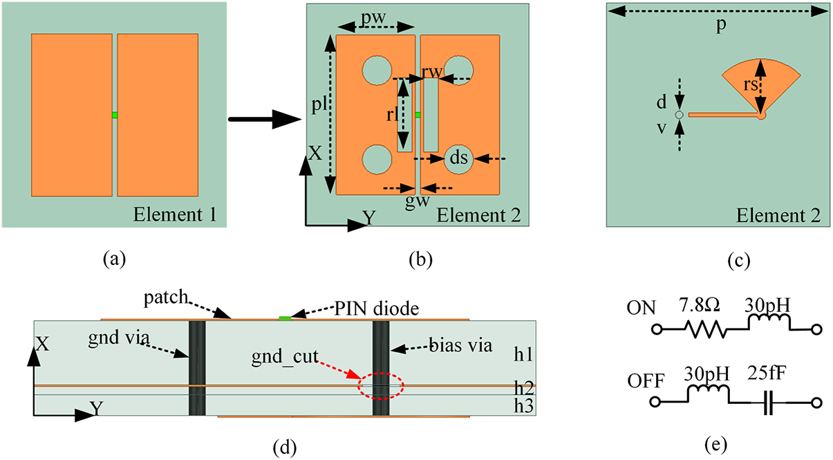
The wideband 1-bit design process of the proposed element configuration can be seen in Fig. 1. The configuration includes three layers of metal, two dielectric substrate layers, and a single prepreg layer. There is no airgap between two dielectric layers used for this element, Rogers RO4003 ( $\varepsilon _{r} = 3.55$,
 $\tan \delta = 0.0027$) with thickness of
 $\mathrm{h}1 = 1.524\,\mathrm{mm}$ and FR-4 (
 $\varepsilon _{r} = 4.3$,
 $\tan \delta = 0.02$) with thickness of
 $\mathrm{h}3 = 0.5\,\mathrm{mm}$ are bonded together with thick FR-4 layer which have thickness of
 $\mathrm{h}2 = 0.2\,\mathrm{mm}$. Firstly a simple 1-bit element based on rectangle patch is designed with circle slots and divide it into two patches and integrated PIN diode at center of the patches can be seen in Fig. 1(a). These connected patches serve as a scatterer when illuminated by an incoming wave. The right-side patch is connected with bias via to provide DC supply while the left side patch connected to the ground. Thus, with the state ON “1” or OFF “0” switching of the PIN diode, there are two resonance states excited accordingly. To broaden the bandwidth slots are added can be seen in Fig. 1(b). These slots are strategically placed to modify the current distribution across the patch. This modification can bring a flatter frequency response and improved bandwidth characteristics. The proposed Element2 depicted in Fig. 1(b), is the combination of rectangular and circle slots which further diversifies the current distribution and optimizing bandwidth. The two through holes are designed between the patch and bias circuit. To further choke high frequency circuit, a radial stub and quarter-wave length microstrip line have been designed on the lower most layer to provide the necessary voltage for DC supply can be seen in Fig. 1(c). The ground layer is drilled with a via of 0.45 mm to prevent the via from causing a short circuit to ground at the bias position, while the second via connected to the ground can be seen in Fig. 1(d).
Structure of the 1-bit RRA element. (a) Basic structure. (b) Structure with circle and rectangle slots (c) bottom layer. (d) Front view. (e) Equivalent circuit of PIN diode. p = 12 mm,  $p_w=8.8$ mm,
 $p_l=8.6$ mm,
 $r_w=0.8$ mm,
 $r_l=4$ mm,
 $g_w=0.3$ mm,
 $r_s=3$ mm,
 $d_s=1.6$ mm,
 $d_v=0.4$ mm.

In the design of the proposed wideband element, the dimensions of the rectangular patch are specifically optimized to achieve a phase shift of  ${180^\circ \pm 20^\circ}$. Even minor deviations from these dimensions could disrupt the required phase shift. We choose the high frequency and low loss MADP-000907-14020x PIN diode [Reference Ning, Zhu, Chu, Zou, Zhang, Jinxin, Xiao and Gaosheng13]. The equivalent circuit of the PIN diode can be seen in Fig. 1(e). For forward bias, the PIN diode is simulated as lumped resistance with the typical value of
 $\mathrm{R} = 7.8\Omega$ and an inductance of
 $\mathrm{L} = 30\,\mathrm{pH}$, whereas for reverse bias, it serves as an inductance of
 $\mathrm{L} = 30\,\mathrm{pH}$ and a lumped capacitance with the typical value of
 $\mathrm{C} = 0.025\,\mathrm{pF}$.
Analysis of current distribution patterns across the element designs reveals significant differences when element is illuminated by normal y-polarized waves can be seen in Fig. 2. Element1 consist of a simple patch with a central PIN diode, exhibits edge-constrained current distribution in the OFF state, limiting radiation performance. When activated, the current distribution becomes more uniform. Element2 improves the design, enhancing the efficiency of current flow. It demonstrates the most uniform current distribution and highest efficiency, particularly in the ON state, outperforming element1. The analysis reveals that the integration of design features, such as slots, notably enhances the performance of reconfigurable antennas. Slots facilitate improved current distribution, reduce segmentation, and strengthen coupling with electromagnetic waves, leading to increased radiation efficiency. The simulated results of reflection magnitude and phase performance comparison between two elements evaluated to assess their suitability can be seen in Fig. 3. The simulation results indicate that low reflection magnitude, wide bandwidth and phase difference of the proposed Element2 can be effectively suppressed compare to Element1.
Current distribution patterns comparison between patches at 12.5 GHz when ON and OFF. (a) Element1. (b) Element2.

Simulated results of reflection magnitude and phase performance comparison between Element1 and Element2 of the 1-bit RRA element.

After carefully doing the parametric analysis the simulated results of the reflection phase and reflection magnitude of the proposed 1-bit RRA element under both ON and OFF states of the diode are presented in Fig. 4. Additionally, these results have been validated with ADS, and Fig. 4, compares the outcomes from HFSS and ADS simulations. The figure makes it clear that for proposed Element2  ${180^\circ \pm 20^\circ}$ phase difference between 11.27 and 13.74 GHz is obtained, resulting in 19.75% relative bandwidth and the reflection loss is 1.5 dB at the central frequency of 12.5 GHz. The simulation results indicate that low reflection magnitude and wide bandwidth of the proposed Element2 can be effectively suppressed compare to Element1. The results demonstrate the wideband capability and reconfigurable performances of the element. The proposed RRA element meets our design expectations. The flexible design is ensured by the RRA element overall satisfactory performance.
Simulated results of reflection magnitude and phase performance of the proposed element comparison between HFSS and ADS of the 1-bit RRA element.

The proposed 1-bit RRA element has been simulated under floquet port and periodic boundary conditions. The simulated results under the normal incidence angle  ${0^\circ}$ to incidence angle
 ${30^\circ}$ can be seen in Fig. 5. It can be observed that the cell performance undergoes only a small variation as compared to that at the normal incidence. At the incident angle
 ${30^\circ}$ the magnitude variation is 0.2 dB, indicating that each element’s reflective magnitude is almost equal. While at the incident angle
 ${30^\circ}$ the reflective phase variation is approximately
 ${24^\circ}$, indicating a stable phase distribution for the proposed element design. The results demonstrate the wideband capability, oblique incidence and reconfigurable performance of the element.
Simulated oblique incidence performance of the RRA element.

Design and optimization of RRA
Based on the proposed 1-bit wideband RRA element, a  $14 \times 14$ square aperture is designed. The entire aperture size of the RRA is approximately
 $200 \, \text{mm} \times 200 \, \text{mm}$ while the effective aperture area is
 $7\lambda_{0}^{2}$ with total 196 PIN diodes. The standard feeding horn is employed as a feed source to illuminate the RRA, which corresponds to a source with radiation pattern characterized by
 $\cos^q \theta$ (q = 5.575). The feeding horn focal height from phase center to the RRA is 152 mm to provide maximum illumination efficiency and spillover efficiency [Reference Ang, Yang, Elsherbeni, Huang and Rahmat-Samii23]. The F/D ratio is 0.9. Furthermore, in order to increase the aperture efficiency and reducing the feed blockage, the feeding horn is titled from the center point of the aperture and the angle of the offset degree has been set as
 ${17^\circ}$ placed in the H-plane from the center of RRA.
Once the placement of the feeding horn and the dimensions of the aperture have been determined, the initial required phase adjustment for the coordinates  $(\theta_0, \phi_0)$ and the phase shift of the ijth element are computed using the following method:
 \begin{equation}
\phi_{1-\text{bit}}(ij) = k\left({\mathbf{Q}}_{ij} - \hat{\mathbf{z}}_0 \cdot \vec{\mathbf{q}}_{ij}\right) + \Delta_\phi.
\end{equation}
where k is refer to the free space wavenumber,  ${\mathbf{Q}}_{ij}$ is the spatial distance from the feed to the ijth element,
 $\vec{\mathbf{q}}_{ij}$ is refer to the position vector to the ijth element and
 $\hat{\mathbf{z}}_0$ represents the unit vector in the main beam angle
 $(\theta_0, \phi_0)$. Furthermore
 $\Delta_\phi$ represents a constant reference phase used for additional optimization of the steering beams. The Eq (1) allows for continuous phase shift adjustments ranging from 0∘ to 360∘, where every element has only two possible states. Here we are using RRA elements with 1-bit phase resolution values 90∘ and 270∘ with a standard 180∘ to quantize phase shifts. The quantized phase can be obtained as follows,
 \begin{equation}
\phi_{ij}^q = \begin{cases}
90^\circ, & 0^\circ \leq \phi_{1-\text{bit}}(ij) \lt 180^\circ \\
270^\circ, & 180^\circ \leq \phi_{1-\text{bit}}(ij) \lt 360^\circ
\end{cases}.
\end{equation}
Equations (1)–(2) can therefore be used to determine the phase shift distribution across various scanning angles at the operating frequency. Apart from that, Equation (2) could be used to accomplish quantization in order to retrieve the array’s 1-bit phase distribution, specifying the particular state (ON or OFF) of the diodes in the element. The continuous phase pointing in the  $(\theta_{0^{\circ}}, \phi_{0^{\circ}})$ beam direction at various scanning angles can be seen in Fig. 6. The reflectarray overall phase errors are to be reduced with the help of this phase optimization.
Phase distribution at different scanning angles (a)  $(\theta_{0^{\circ}}, \phi_{0^{\circ}})$. (b)
 $(\theta_{40^{\circ}}, \phi_{0^{\circ}})$. (c)
 $(\theta_{-30^{\circ}}, \phi_{90^{\circ}})$. (d)
 $(\theta_{-40^{\circ}}, \phi_{0^{\circ}})$.

Simulated and measured results
To verify the performance of fabricated prototype RRA, the experiment is conducted in an anechoic chamber with a setup of vector network analyzer setup, DC bias micro-controller circuit board with power supply, 3D holder with array and receiving horn are depicted in Fig. 7. A DC bias board is mounted on the rear side of the ground area. The DC bias configuration for each element consists of a thin DC line and FPC socket. There are 14 FPC sockets welded on the back side of the RRA to connect the biasing lines and control circuit board, which are distributed on the right and left of the reflectarray. To determine the effective operational performance of the designed RRA for adaptive beam scanning, the measured and simulated patterns of the RRA operating at 12.5 GHz are presented in Fig. 8. At each scanning angle, the main beams are aligned to specified angles according to computed coding sequences. Because of the symmetrical phase distribution and configuration of the feed horn, the scanning beams exhibit almost minimal variation at both planes.
Employing a deviated feed horn helps mitigate the blocking effect on the RRA when radiating at wide scanning angles. Furthermore, careful selection of a suitable reference phase  $\Delta\phi$ can balance the gain distortion due to phase errors across various scanning angles. Moreover, with the low reflection loss element, the RRA can maintain minimal gain loss within a scanning range of
 $\pm50^\circ$ in a 2D plane. The measured gain reduction across the scanning range is approximately 1.88 dB along the E-plane and 2.21 dB along the H-plane. Furthermore, the measured gain for the broadside beam is 21.1 dB with a indicative aperture efficiency of approximately 20.9%. The primary cause of the minor discrepancy within the simulated and measured results is due to the inevitable misalignment that occurred during the experimental setup between the horn antenna and the array prototype. Moreover, the findings reveal that positioning the feed horn in the H-plane introduces a blocking effect due to the offset feed, which results in high sidelobe levels (SLL).
Fabricated view of array with 3D holder, control board, DC lines and receiving horn.

Simulated and measured radiation gain patterns of RRA for 1-bit beam scanning. (a) E-plane. (b) H-plane.

To further explore the capabilities of the proposed RRA, simulations were conducted for beam scanning up to  $\pm60^\circ$. The simulated results, as shown in Fig. 9, indicate that the RRA can theoretically achieve beam steering at these wider angles. However, the gain reduction at
 $\pm60^\circ$ exceeds 3 dB in both the E-plane and H-plane, primarily due to increased path length differences and phase errors at extreme angles. Additionally, practical limitations in the experimental setup, such as feed blockage and alignment inaccuracies, made it challenging to obtain reliable measured results for
 $\pm60^\circ$. These findings highlight the trade-off between scanning range and radiation efficiency in the proposed design. As a result, the RRA exhibits superior beam-scanning capabilities in the E-plane, where there is no feed blockage. This absence of obstruction in the E-plane also results in lower SLL compared to the H-plane, further enhancing overall performance. Despite these factors, the overall consistency within the measured and simulated results is maintained. These results demonstrate a good agreement between the simulated and measured values. The tested results also evaluates the bandwidth performance of the
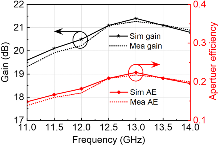
 $14 \times 14$ RRA, analyzing radiation gain and aperture efficiency across various frequencies, as shown in Fig. 10. The gain remains consistent within the desired frequency range. The measured 1 dB gain bandwidth ranges from 12.03 to 14 GHz, achieving a relative bandwidth of 15.1%, highlighting the wideband performance of the proposed RRA compared to conventional approaches. The proposed RRA performs in an enhanced manner compared to the recent 1-bit RRA reported in the literature, in terms of element bandwidth, phase, peak gain, aperture efficiency, as well as radiation gain steadiness across the scanning range. These advancements, clearly demonstrated in Table 1, represent a significant step forward in RRA.
Simulated radiation gain patterns of RRA for 1-bit beam scanning. (a) E-plane. (b) H-plane.

Simulated and measured radiation gain patterns of RRA for 1-bit beam scanning.

Comparison of antenna array performance with state-of-the-art designs

a AE: Aperture efficiency
b N/A: Not available
Conclusion
In this paper, we propose a wideband RRA element using 1-bit resolution for 2D beam scanning capability at the Ku-band. It consists of two relatively simple metallic patches with slots. By carefully controlling these patches, the 180∘ phase difference using a single PIN diode is achieved with a corresponding wide bandwidth of 19.75%. Furthermore, a wideband  $14 \times 14$ RRA is tested and measured. Measured results show that beam scanning in 2D plane within the range from
 $\pm50^\circ$ could be achieved. The maximum gain reduction is 1.88 dB in the E-plane and 2.21 dB in the H-plane within the
 $\pm50^\circ$ scanning range. The 1-dB gain bandwidth of RRA is 15.1%. These findings highlight the trade-off between scanning range and radiation efficiency in the proposed design. Future work could focus on optimizing the element design and feed configuration to mitigate losses at extreme angles, enabling broader coverage while maintaining high gain and efficiency. The proposed design, with its low power consumption and cost-effectiveness, is a promising candidate for wireless communication, sensing, and imaging applications.
Data availability statement
The data that support the findings of this study are available from the corresponding author upon reasonable request.
Acknowledgements
This work was supported by the National Natural Science Foundation of China (NSFC) under Grant 62321001.
Competing interests
The authors affirm that they do not possess any identifiable financial conflicts of interest or personal connections that might have seemed to exert an influence on the research presented in this paper.

Zahid Iqbal received the B.S. degree in electrical technology from Government College University Faisalabad, Pakistan, in 2017, and the M.S. degree in electrnics and communication engineering from Beijing University of Posts and Telecommunications, Beijing, China in 2020, where he is currently pursuing the Ph.D. degree with the School of Electronic Engineering and the Beijing Laboratory of Work Safety Intelligent Monitoring. His current research interests include reconfigurable antennas, wideband antennas and reflectarray antennas.

Xiuping Li received the B.S. degree from Shandong University in 1996, the Ph.D. degree from Beijing Institute of Technology in 2001. From 2001 to 2003, she joined in Positioning and Wireless Technology Center, Nanyang Technological University in Singapore, where she was a research fellow and involved in the research and development of RFID system. In 2003, she was a research professor in Yonsei University, Seoul, South Korea. Since 2004, she joined Beijing University of Posts and Telecommunications as associate professor, and promoted to professor in 2009. She has been selected into the New Century Excellent Talents Support Plan in National Ministry of Education, the Beijing Science and Technology Nova Support Plan, in 2007 and 2008 respectively. She won the second prize of the Progress in Science and Technology of China Institute of Communications and the Excellent Achievements in Scientific Research of Colleges and Universities in 2015 and 2018, respectively. She is the author of 4 books, over 200 journal and conference papers. She is also awarded more than 20 PRC patents. Her current research interests include millimeter-wave antennas, THz antennas, RFID systems, and MMIC design.

Zihang Qi received the B.E. degree in electronic and information engineering from China Three Gorges University, Yichang, China, in 2013, and the Ph.D. degree in electronic science and technology from the Beijing University of Posts and Telecommunications, Beijing, China, in 2019. He is currently an associate research fellow with the Beijing University of Posts and Telecommunications. His current research interests include OAM antennas, millimeter-wave/THz antennas and microwave filters.

Wenyu Zhao received a B.S. degree and Ph.D. degree from the Beijing University of Posts and Telecommunications, Beijing, China, in 2018 and 2023, respectively. He is currently a post-doctoral with the School of Electronic Engineering and the Beijing Key Laboratory of Work Safety Intelligent Monitoring at the Beijing University of Posts and Telecommunications. His current research interests include dual-polarized antennas, millimeter-wave antennas, and reflect array antennas.

Zaid Akram received the B.Eng. degree, in 2012, and the Ph.D. in Electronic Science and Technology from the Beijing University of Posts and Telecommunications, China, in 2021. He is currently a research assistant with James Watt School of Engineering, University of Glasgow, UK. His current research interests include millimeter-wave/THz reconfigurable metasurface, wideband antenna and integrated sensing and communication.

Yaohui Niu received the B.E. degree from Beijing University of Posts and Telecommunications, Beijing, China, in 2020, where he is currently pursuing the Ph.D. degree with the School of Electronic Engineering. His current research interests include RFID antennas, millimeter-wave antennas, phased array and metasurface antennas.

Muhammad Ishfaq received a B.S. degree in electrical engineering in 2009 and an M.S. degree in electrical engineering, with a specialization in signal processing and wave propagation, from Linnaeus University, Vaxjo, Sweden, in 2013 supplemented by participation in Europe’s Erasmus Exchange Program (MS) Université de Technologie de Belfort Montbéliard (UTBM), Belfort, France. He received the Ph.D. degree in electronics engineering from the Beijing University of Posts and Telecommunications, Beijing, China in 2024. He is currently a postdoctoral with the School of Electrical and Information Engineering at the Lanzhou University of Technology, Lanzhou, China. His current research interests include OAM antennas, RIS antennas, and transmitarray/reflectarray metasurfaces.