I. INTRODUCTION
Shape memory alloy (SMA) thin films based on nickel-titanium (NiTi) alloys of near equiatomic compositions have received considerable attention because of their potential for applications in microelectromechanical systems (MEMS) devices such as microactuators, microvalves and microgrippers.Reference Wayman and Tsakalakos1–Reference Kahn, Huff and Heuer4 These shape memory thin films exhibit higher work density and larger recoverable strain as compared with other competing materials such as electrostatic, electromagnetic and piezoelectric materials.Reference Jardine, Mercado, Atzmon, Greer, Harper and Libera5 However, to use a NiTi film in microactuator applications, a precise control over its composition, structure and microstructure (hence its transformation temperature) and a good mechanical response is a prerequisite.
In NiTi alloys, the shape memory effect arises due to the reversible phase transformation from high-temperature austenite (B2) phase to low-temperature martensite (B19′) phase. Thus NiTi films have to be in crystalline form to show the shape memory effect. However, NiTi films produced by sputter deposition at low ambient conditions are usually amorphous in nature.Reference Seguin, Vendan, Isalgue, Esteve-Cano, Carchano and Torra6 Therefore, these films have to be annealed above their crystallization temperature to crystallize them.Reference Yang, Jia, Zhang, Shen, Hu and Wang7, Reference Bush, Johnson, Lee and Stevenson8 The effect of annealing temperature on the phase transformation behavior of NiTi alloy is very well established in the literature.Reference Huang and Liu9–Reference Satoh, Birnbaum and Yao11 Annealing treatment often results in oxidation of these films especially if the vacuum is not very high. The high-temperature oxidation behavior of equiatomic bulk NiTi alloys has been investigated in previous studies.Reference Chu, Wu and Yen12–Reference Wang, Mao, Cao, Qing, Jiang and Peng15 It has been reported that a multilayered scale consisting of an outer rutile layer (TiO2), an inner Ni3Ti layer and an intermediate layer mixed with TiO2 and NiTi is formed during thermal oxidation of bulk NiTi alloy. Compared with relatively dense bulk materials, sputter-deposited Ti–Ni thin films are often porous with microcracks and voids.Reference Miyazaki and Ishida16–Reference Huang, Liu, Wilson and Varadan18 These microdefects derived from the vapor supply and surface mobility of atom during sputtering provides short circuit pathways for the inward diffusion of oxygen during oxidation.Reference Badini and Laurella19 Thus the oxidation behavior of Ti–Ni thin films, such as the formation and growth of the oxide scale, the in-depth diffusion of oxygen and the distribution of oxides may differ from that of bulk Ti–Ni materials.
No systematic investigation has been carried out in literature on the effect of annealing on oxidation and its consequent effect on microstructure and mechanical properties in NiTi films. Hence, in this work, the effect of annealing temperature on oxidation and its consequent effect on microstructure and mechanical properties in NiTi film deposited on silicon substrates by DC magnetron sputtering were studied.
II. EXPERIMENTAL
A. Film deposition
Thin films of NiTi were deposited by DC magnetron sputtering from a NiTi alloy target (48:52: Ni:Ti at.%) on (100)-oriented Si wafer substrate heated to 300 °C. Argon was used as sputtering gas at a working pressure of 1.5 x 10⁻³ mbar. Prior to film deposition, the oxide layer and other target contaminations were minimized by pre-sputtering of the alloy target in a closed shutter position. The pre-sputtering was carried out for 15 min. The film thickness was measured by creating a step on the substrate and measuring the step height using a surface profilometer. The thickness of the deposited films was ∼1 μm. The composition of the films determined by Rutherford backscattering (RBS) technique was found to be Ni-49 at.% Ti. The variation of film composition with depth was investigated by Secondary Ion Mass Spectroscopy (SIMS) analysis. The films deposited at 300 °C were subsequently annealed at different temperatures viz., 300, 500, 600 and 650 °C for 4 h at a vacuum of 10−6 mbar. The temperature was raised to the annealing temperature at a ramp rate of 50 °C/min.
B. Transmission electron microscopy (TEM)
The microstructure of the films was characterized by TEM of cross-sectioned specimens. Cross-sectional TEM (XTEM) specimens were prepared by a standardized cross-sectioning technique. A Tecnai G2 30ST analytical transmission electron microscope (AEM) equipped with ‘EDAX’ x-ray energy dispersive spectrometer (EDS) was used for conventional TEM and nanoscale composition analysis of the deposited films. Scanning transmission electron microscopy–x-ray energy dispersive spectrometry (STEM-EDS) spectrum imaging technique was used to reveal elemental distribution and composition profile across the film thickness and the film–substrate interface.
C. Nanoindentation
In the present work, all nanoindentation studies were performed using a Nanoindenter from CSM Instruments, with a three-sided pyramidal Berkovich diamond indenter having an included angle of 142.3° between the opposite faces. First, tests were performed over a range of loads to identify the load where the depth of indentation is such that it is significantly more than the surface roughness but less than the film thickness to ensure that there is no substrate effect. In all the tests, films were loaded to the maximum load and were held constant for 10 s at maximum load followed by unloading. The loading and unloading rates for all the nanoindentation tests were kept constant at 6 mN/min. More than 20 tests were performed for each NiTi film. Atomic force microscope (AFM) was used to measure the surface roughness of thin films prior to nanoindentation tests as well as after the nanoindentation tests to examine the residual indents for sink-in or pile-up.
III. RESULTS
A. TEM studies of annealed NiTi thin films
TEM studies of the cross-sectioned samples were carried out to reveal the microstructure across the film thickness. The salient results pertaining to the films annealed at different temperatures are presented below.
1. NiTi thin film deposited at 300 °C
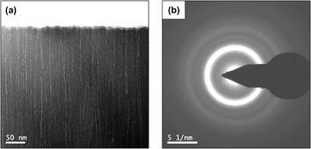
It should be noted that the as-deposited (at 300 °C) film was amorphous in nature and the films subsequently annealed at 300 for 4 h showed no significant crystallization. Since there is no change in the features, the TEM micrograph for only the film after annealing for 1 h is shown in Fig. 1. It can be observed that both the as-deposited and as-deposited and annealed films exhibit a nearly featureless morphology, which is typical of amorphous materials [Fig. 1(a)]. This is confirmed by the selected area diffraction pattern (SADP) shown in Fig. 1(b). However, fine porosity in the form of nanochannels, only a few nanometers in width, running from top to bottom of the film perpendicular to the Si substrate were observed. The fine columnar structure is a growth morphology, which has been reported to evolve due to reduced surface diffusion of the atomic species under higher argon pressure during sputter deposition and a similar microstructure was observed earlier.Reference Chu, Lai, Lin and Wang20, Reference Eswar Raju, Bysakh, Sumesh, Kamat and Mohan21 These nanochannels remained undisturbed in spite of annealing at higher temperatures, as will be shown in Sec. III. A. 2–Sec. III. A. 5.
XTEM results of the film annealed at 300 °C: (a) bright-field TEM image of top part of film cross-section, (b) SAD pattern of the film.

2. NiTi thin film annealed at 500 °C
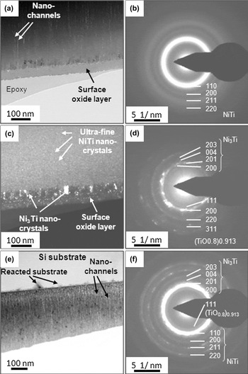
Figure 2(a) is the bright-field TEM image showing the cross-section nanostructure near the top surface of the film annealed at 500 °C. The upper part of the film exhibits a nearly featureless morphology, except for the nanochannels running from top to bottom of the film perpendicular to the Si substrate, which can be attributed to the alignment of fine porosity. Such nanoscale columnar morphology existed in the as-deposited film as mentioned earlier, and notably, remained undisturbed. In addition, a distinct layer of about 60 nm thickness on top of the film surface can be very clearly seen. This formation of oxide layer on film surface is also supported by SIMS studies. SIMS data show that the oxide layer thickness increased from 10 nm to 60 nm as the annealing temperature was increased from 300 to 500 °C. EDS composition analyses at many locations along the top layer revealed that this layer contains titanium and oxygen. Just underneath this surface oxide layer, a layer of similar thickness showing a dark contrast can be observed. The SADP taken from the NiTi film [Fig. 2(b)] shows several broad rings. This is suggestive of the presence of extremely fine nanocrystals within the otherwise amorphous matrix of the film. The ‘d-spacing’ values calculated from the ring diameters correspond to the reflections of B2 austenitic NiTi phase. The dark-field TEM image [Fig. 2(c)] formed by selecting a part of the first strongest diffraction ring in the SADP clearly reveals the very fine nanocrystals within the amorphous NiTi film. Also revealed are nanocrystals of different sizes present in the two distinct oxidized layers on the film surface. The characteristic SADP [Fig. 2 (d)] from the oxidation-affected surface layers shows both smooth rings and spots, which are from the topmost oxide layer and the underlying nanocrystalline layer, respectively. Analysis of this composite diffraction pattern suggested that the smooth rings correspond to (TiO0.8)0.913 oxide phase, whereas the spots have been identified as the reflections from the Ni3Ti phase in nanocrystalline form present in the underlying thin layer. The bottom half of the film thickness near the Si substrate, the NiTi film showed a coarser nanocrystalline microstructure in the bright-field TEM image [Fig. 2(e)]. The corresponding SADP in Fig. 2(f) shows smooth and spotty rings, which can be indexed for B2-NiTi and Ni3Ti phases, respectively. Small triangular or pyramid-shaped reaction zones grown from the interface into the Si substrate can also be observed. Correspondingly, a modulation in contrast can be observed within the NiTi film adjacent to the substrate. However, they are too small for obtaining SADP for structural information.
XTEM results of the film annealed at 500 °C: (a) bright-field TEM image of the film section near the top surface; (b) selected area diffraction (SAD) pattern from near the top surface of the film showing halo and several rings, suggesting the presence of fine nanocrystals in otherwise amorphous film; (c) dark-field image reveals nanocrystals in the surface oxide layer; (d) SADP from the oxide layer containing (TiO0.8)0.913 oxide phase; (e) bright-field image showing the bottom part of the film containing well-formed nanocrystals and reaction pyramids at the film–substrate interface; and (f) SAD pattern from the bottom part of the film showing diffraction rings of NiTi and Ni3Ti.

3. Ni-Ti thin film annealed at 600 °C
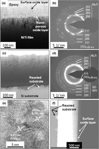
The results of cross-section TEM characterization of the film annealed at 600 °C are presented in Fig. 3. The bright-field TEM image [Fig. 3(a)] shows the cross-section microstructure near the top surface of the film. In this case, three distinct oxidized layers can be seen very clearly. A top oxide layer of about 100 nm thickness with considerable surface roughness, an intermediate layer of about 25 nm thickness with occasional nanoporosity along its interface with the topmost oxide layer and the 50 nm thick bottom layer exhibiting nanocolumnar nanoporous structure. Nanoprobe STEM-EDS analyses of these three layers revealed that the oxygen concentrations in these three TiOx layers are different. Local variations in concentration across the thickness of each layer were also detected. The SADP given in Fig. 3(b) was obtained by selecting the top columnar portion of the film, just below the surface oxidation layers. The spotty diffraction rings are the reflections from the relatively large Ni3Ti nanocrystals just below the oxide layer. However, the smooth broad rings can be indexed for the (TiO0.8)0.913 oxide phase. The broad nature of the rings suggests extremely fine size of the nanocrystals of this suboxide, which coexists with the coarser Ni3Ti at the top part of the metallic film. The TEM micrograph form the lower part of the film is shown in Fig. 3(c). The SADP [Fig. 3(d)] taken from this region shows several broad rings although they are more spotted than those in case of 500 °C annealed film. This is suggestive of the presence of nanocrystals, albeit coarser, compared with those seen in the film annealed at 500 °C. The ‘d-spacing’ values calculated from the ring diameters also correspond to the reflections of B2 (austenite) NiTi phase and Ni3Ti phase. The high-resolution electron microscopy (HREM) image in Fig. 3(e) shows the lattice fringes from the nanocrystals and the granular phase-contrast from the residual amorphous phase. The triangular shaped reaction zones growing from the interface into the Si substrate revealed in the high angle annular dark-field (HAADF) image [Fig. 3(f)] are found to have become larger on annealing the film at 600 °C. Since HAADF image shows Z-contrast, it suggests that the triangular or pyramid-shaped reaction zones are enriched with heavier elements, as will be shown subsequently. The image also reveals composition modulations resulting in layers of different compositions parallel to the substrate.
XTEM results of the film annealed at 600 °C: (a) bright-field TEM image of top part of film cross-section showing the microstructure of the oxidation layer, (b) SAD pattern from the film just beneath the oxide scale, (c) TEM image from the bottom part of the film close to Si substrate, (d) the corresponding SADP from the film. (e) high-resolution electron microscopy (HREM) image of the film showing lattice fringes in the nanocrystals, and (f) high-angle annular dark-field imaging (HAADF) image reveals z-contrast modulation across the film thickness indicating variation in concentration of the constituent elements in different layers.

4. Ni-Ti thin film annealed at 650 °C
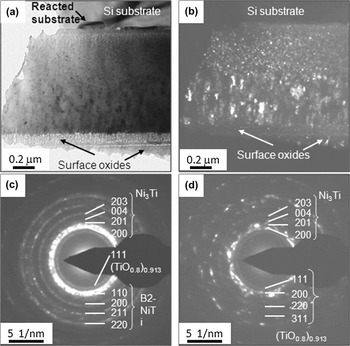
A representative bright-field TEM image of the entire film cross section is shown in Fig. 4(a). Notably, two distinct microstructures can be observed across the film thickness. The top half of the thickness shows larger columnar grains, whereas the bottom half shows a microstructure composed of equiaxed nanocrystals. The dark-field image in Fig. 4(b) shows this difference more clearly. Electron diffraction patterns from the bottom half and top half of the film, just underneath the oxidation-affected surface layers, are shown in Figs. 4(c) and 4(d), respectively. These SADPs from the NiTi film show several broad rings although they are much more spotted than those observed in the films annealed at 500 and 600 °C. This is suggestive of significant coarsening of the nanocrystalline grains. In this case as well, the calculated ‘d-spacings’ from the ring diameters correspond to the reflections of B2 NiTi phase and Ni3Ti phase. The diffraction rings in Fig. 4(c) can be indexed as the reflections from both B2-NiTi and Ni3Ti. The pattern in Fig. 4(d), however, suggests the presence of primarily Ni3Ti, along with a small amount of the fcc-oxide (TiO0.8)0.913. At or near the interface, the triangular shaped reaction zones growing from the interface into the Si substrate seen in the film annealed at 500 °C and 600 °C are seen to have become even larger on annealing the film at 650 °C.
XTEM results of the film annealed at 650 °C: (a) bright-field, (b) dark-field TEM images at low magnification reveal two distinct microstructures of the top and bottom halves of the film cross-section, (c) SADP from bottom half suggests coexistence of B2-NiTi and Ni3Ti, and (d) SADP from the top half of the film suggesting Ti-oxide coexisting with coarse Ni3Ti.

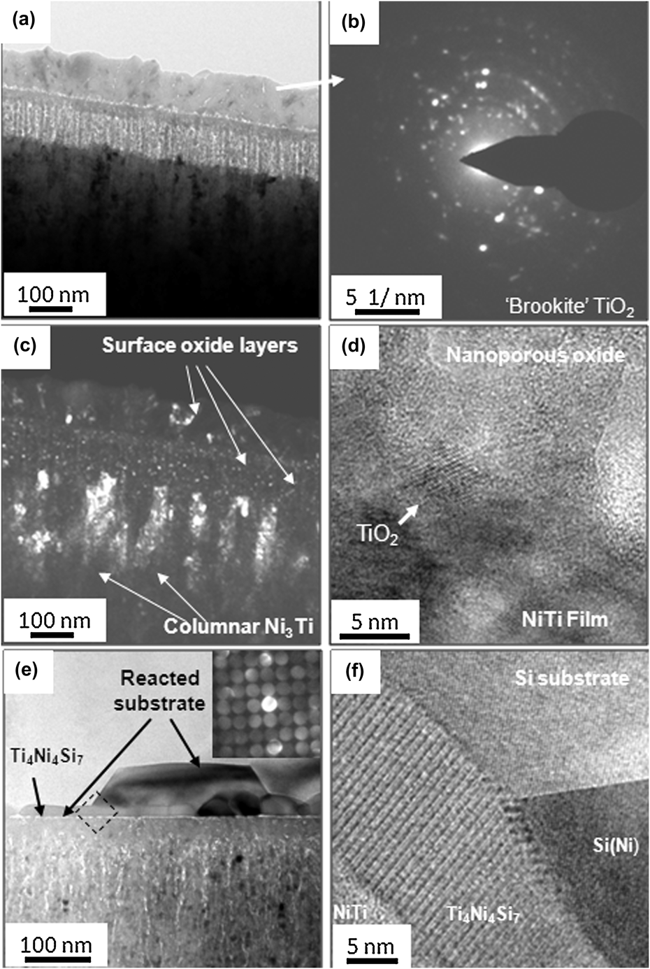
The high magnification bright-field TEM image in Fig. 5(a) shows the top portion of the film that was annealed at 650 °C with the surface oxide layers. The oxidation layer on film surface of the film annealed at 650 °C is much thicker compared with the oxidation layers on respective film surfaces of the films annealed at 500 and 600 °C. Interestingly, it is the nanoporous nanocolumnar TiOx layer that has grown significantly more than the other two layers. The topmost layer has developed a greater crystallinity as suggested by the bright-field image and confirmed by the spotty SAD pattern Fig. 5(b), and the corresponding dark-field image in Fig. 5(c). Analysis of the pattern suggests the formation of Brookite phase. Figure 5(d) is the HREM image showing a TiO2 nanocrystal at the film–nanoporous oxide interface.
XTEM results of 650 °C annealed film (contd.): (a) bright-field image at higher magnification reveals three distinct oxide layers, (b) SADP from the topmost oxide layer suggesting Brookite TiO2, (c) dark-field image revealing columnar Ni3Ti crystals in the film and fine nanocrystals in the oxide layers, (d) HREM image shows lattice fringes in a TiO2 nanocrystal at the interface of film and nanoporous oxide, (e) BF image showing reaction layers at the film–substrate interface. Inset: microdiffraction along [001] zone of the Ti4Ni4Si7 layer and (f) HREM image showing ordered lattice structure of Ti4Ni4Si7 at the interface.
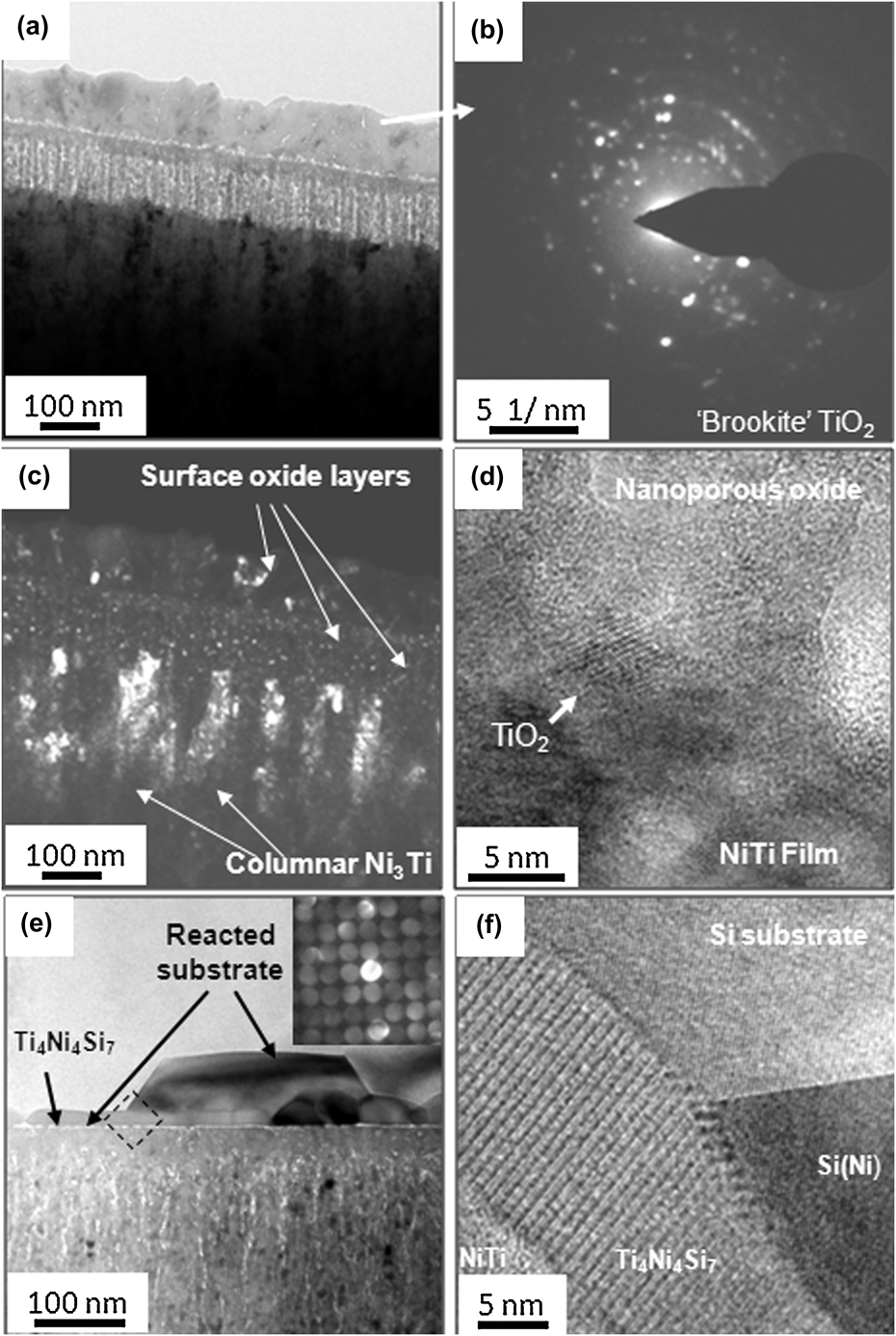
Annealing at 650 °C results in two layers of reaction products at the film–substrate interface being formed as shown clearly in the high magnification Bright-field TEM image [Fig. 5(e)]. The inset of this figure shows the microdiffraction pattern from the reaction layer next to the film interface. The pattern can be indexed as the [001] zone axis of tetragonal Ti4Ni4Si7 intermetallic compound. EDS composition analysis suggests a composition of about Si-19Ti-22Ni (at.%), which is close to that of Ti4Ni4Si7. The trapezoid-shaped feature, however, contain mainly Ni with a composition of about Si-25at.%Ni (Si3Ni), though the cubic structure is retained. Jarrige et al.Reference Jarrigea, Holligerb, Nguyenc, Ip and Jonnard22 and Fenske et al.Reference Fenske, Schöpke, Schulze and Selle23 also reported the formation of silicide (Si3Ni) at film–substrate interface. The HREM image from the boxed area in Fig. 4(e) of the film–substrate interface region is presented in Fig. 5(f). The portion of the trapezoid feature is seen to maintain epitaxial relation with the (111) planes of the parent Si substrate. The Ti4Ni4Si7 intermetallic layer shows periodic modulation of lattice image contrast typical of chemically ordered atomic layers present in intermetallic compounds.
5. STEM-EDS composition mapping of annealed Ni-Ti thin films
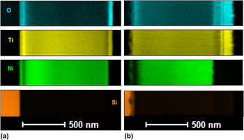
To better understand the oxidation behavior, STEM-EDS composition mapping was carried out for the ‘as-deposited’ as well as for all the annealed films using nanoprobe electron beam in the TEM. The STEM-EDS characteristic x-ray elemental maps are presented in Figs. 6(a) and 6(b) for films annealed at 500 °C and 650 °C, respectively. The maps reveal distinct layers of different composition and therefore, the distribution of different elements present in these layers of varied concentrations. The quantitative maps also reveal the nanothreads of high and low Ni concentration running across the film thickness and roughly perpendicular to the substrate surface.
STEM-EDS characteristic x-ray elemental maps of the cross-sectioned film annealed at (a) 500 °C and (b) 650 °C. The maps clearly reveal distinct layers in which Ni, Ti and O are distributed in different proportions.

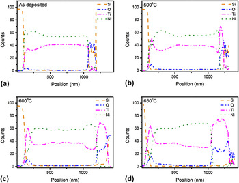
The line-averaged composition (wt%) plots for as-deposited as well as films annealed at 500, 600 and 650 °C are presented in Figs. 7(a)–7(d), respectively. It is evident from Fig. 7(a) that there is no significant oxygen pick-up during the deposition process. From these composition plots, it is also obvious that on annealing, the concentrations of both O and Ti are of maximum value in the topmost oxide layer, which is almost completely depleted of Ni. The nanoprobe STEM-EDS quantitative analysis also revealed large fluctuations in local composition within the porous nanocolumnar TiOx (1.0 < x < 2.0) layer, and the average composition was found to be about TiO1.5. There is also depletion of Ni (more so at 650 °C than at 600 °C and 500 °C) at the silicon-NiTi film interface.
STEM-EDS line-averaged wt% composition profiles for Ni, Ti, O, and Si showing the concentration variation of the respective elements across the film thickness for (a) as-deposited film and the film annealed at different temperatures; (b) 500 °C, (c) 600 °C, and (d) 650 °C.

B. Nanoindentation and atomic force microscopy studies of annealed Ni-Ti thin films
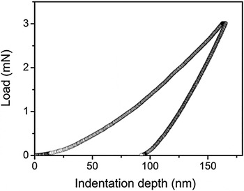
The representative load versus indentation depth plot obtained from a nanoindentation test is shown in Fig. 8. The Oliver and Pharr methodReference Oliver and Pharr24 was used for analyzing the data to obtain hardness and elastic modulus. The hardness is expressed as a ratio of peak load (P max) to the contact area (A c) as given below:

A representative load versus indentation depth plot obtained from a nanoindentation test for as-deposited NiTi film.

where, the contact area (A c) is a function of contact depth (h c):  and the contact depth (hc) is defined as the function of maximum displacement (h max) of the tip (i.e., penetration depth at P max) and unloading stiffness
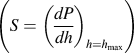 at maximum load:
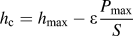 ;
The elastic modulus of the sample (E) is determined by the following equation:

where, ν and νi are the Poisson’s ratio of the sample and indenter, respectively, Ei is the elastic modulus of the indenter material and E eff is the effective modulus of the combined system of indenter and sample, which is defined as: 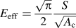
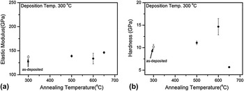
Plots of elastic modulus (E) and hardness (Hv) values derived from nanoindentation experiment, against annealing temperature are presented in Figs. 9(a) and 9(b), respectively. Though the elastic modulus value did not change significantly, the hardness showed an increasing trend up to 600 °C but dropped to a lower value for the annealing temperature of 650 °C.
Plots of (a) elastic modulus and (b) hardness of the films versus annealing temperature.

C. AFM studies of annealed Ni-Ti thin films
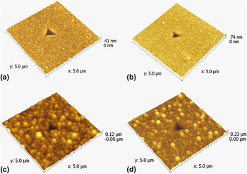
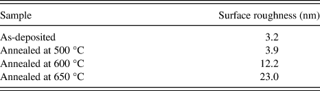
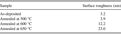
AFM has been demonstrated to be a very versatile and powerful tool for surface imaging at the nanometer level and the revelation of the surface characteristics of the films. Figure 10 depicts the typical three-dimensional AFM images (5 × 5 μm) of Ti–Ni thin films in the as-deposited condition as well as after annealing at different temperatures. The as-deposited Ti–Ni thin film exhibits a relatively smooth surface consisting of coalescent islets [Fig. 10(a)]. As the images show, the film roughness gradually increases with increasing annealing temperature. This is confirmed by the surface roughness values calculated from the AFM images given in Table I. This behavior is contrary to the observations of Zhang et al.Reference Zhang, Xie and Wu25 who observed smoothening of the film surface on thermal oxidation at higher temperatures.
AFM images showing surface morphologies of the films in (a) as-deposited and annealed at (b) 500 °C, (c) 600 °C, and (d) 650 °C conditions.

Variation of surface roughness with annealing temperature.
IV. DISCUSSION
A. Effect of annealing temperature on oxidation and microstructure
The effect of annealing temperature on oxidation and hence the microstructure of NiTi thin film is discussed below. The NiTi film in the as-deposited condition is amorphous and remains so even after annealing it at 300 °C for 1 h. The nanocolumnar morphology with intercolumnar nanochannel porosity observed in the as-deposited film can be attributed to the growth mechanism of the thin film from vapor state. The observation of amorphous nature of the as-deposited (substrate temperature of 300 °C) as well as films which have been annealed for 1 h at 300 °C is consistent with literature as the reported crystallization temperature in these films is ∼483 °CReference Otsuka and Ren26. The absence of any significant oxide layer in the film deposited at 300 °C suggests that these films do not show significant oxidation up to 300 °C for an exposure time of 1 h. Annealing at 500 °C results in partial crystallization of the NiTi film but the film also starts showing effects of oxidation. Oxidation results by the diffusion of oxygen into the film as the initial oxygen content at the film–substrate interface is negligible [Fig. 7(a)]. It should also be noted that there is no Ni oxide formed on the surface. This may reflect the difference in the oxygen affinity between Ti and Ni, i.e., Ti is easily oxidized whereas Ni is more difficult to be oxidized.Reference Chan, Trigwell and Duerig27 Therefore, titanium is oxidized first to form oxide on the film surface whereas Ni remains unchanged. As the oxidation occurs, titanium atoms diffuse outward whereas oxygen atoms diffuse inward. The diffusivity of Ti in TiO2 rutile is faster than that of oxygen.Reference Kekare, Shelton and Aswath28 Hence there is a depletion of Ti and enrichment of Ni just underneath the top oxidized layer. The enrichment of the film in Ni in the upper part of the film should result in the formation and stabilization of B2 NiTi phase at room temperature because the transformation temperature of Ni-rich NiTi compositions is well below room temperature.Reference Otsuka and Ren26 The enrichment of Ni is also expected to result in the formation of Ni3Ti phase. Both the phases are experimentally observed (Figs. 2–5) on annealing at temperatures between 500 and 650 °C. The increase in crystallization and coarsening of the NiTi grains with increasing annealing temperatures is also along expected lines.
Near the substrate, there is a marginal depletion of Ni. Both Ti4Ni4Si7 and Si3Ni are formed at the substrate and film interface. The extent of intermetallic formation is much higher at higher annealing temperatures. It is thus clear that both the thickness of the oxidation layer as well as the reaction zone at the interface of the Si wafer and the film, increase with increase in annealing temperature. This suggests that annealing in these films should be carried out at the lowest temperature possible so that the deleterious effect of oxidation and interfacial reactions can be avoided. However, as mentioned earlier, the crystallinity of the film is an essential requirement for obtaining shape memory effect in these films and it is evident from this study that only partial crystallization occurs at 500 °C, even though it is above the reported temperature of crystallization in these alloys. Thus annealing above 500 °C cannot be avoided. Hence care should be taken to keep the vacuum in the sputtering chamber as high as possible. Also since the best shape memory effect is observed in equiatomic films, it may be advisable to start off with a Ti-rich composition so that most of the film becomes equiatomic after annealing treatment for crystallization.
The results in this study show that NiTi films should be annealed in a narrow temperature range after deposition. The temperature should be greater than the crystallization temperature but not high enough to cause oxidation of the film as this leads to the deterioration of the shape memory properties of the film. Additional research on the effect of vacuum levels during deposition and annealing as well as the effect of capping layer on oxidation behavior is required.
B. Effect of annealing temperature on mechanical properties
As discussed in the previous section, the microstructure of the film is highly inhomogeneous and evolves with change in annealing temperature. Thus the measured mechanical properties by nanoindentation technique are not a reflection of the mechanical properties of NiTi film alone. The measured elastic modulus and hardness reflect a complex interplay of these properties of the individual constituents, their crystallinity and grain size as well as their relative thicknesses for different annealing temperatures and thus it is not at all easy to explain why the mechanical properties behave the way they do with annealing temperatures. However, the observation of a significantly higher measured elastic modulus and hardness values in the present study as compared with those measured in bulk NiTi alloysReference Tall, Ndiaye, Beye, Zong, Soboyejo, Lee, Ramirez and Rajan29 can be attributed to these complex interactions since the elastic modulus and hardness values of titanium oxides are much higher than those of NiTi.
V. SUMMARY
The Ni-49Ti films deposited by DC magnetron sputtering on Si wafers were amorphous in the as-deposited condition and only partially crystallized on annealing at 500 °C. However, at 500 °C, a distinct oxidation layer on the film surface was formed. Small triangular shaped reaction zones growing from the interface into the Si substrate were also observed. With increasing annealing temperature, a gradual increase in thickness and number of layers of various titanium oxide stoichiometries was observed. Growth of triangular shaped reaction zones was also seen with increase in annealing temperature. Nanoindentation studies showed that the film hardness values increase with increase in annealing temperature up to 600 °C and subsequently decrease at 650 °C although it is difficult to ascribe the causes for such behavior because of the complex effects involved.
ACKNOWLEDGMENTS
One of the authors S. Bysakh is grateful to Director, Central Glass and Ceramic Research Institute (CGCRI), Kolkata and two authors (A. Kumar and S.V. Kamat) are grateful to Director, Defence Metallurgical Research Laboratory (DMRL), Hyderabad for giving permissions to publish this paper. The authors also acknowledge the support of Defence Research Development Organization under Project DMR-275 to carry out this research work. The other author (S. Mohan) acknowledges the financial support received from National Program on Smart Materials (NPSM) and Ministry of Communication and Information Technology (MCIT).