I. INTRODUCTION
With continuing device scaling, electromigration (EM) has become a critical reliability concern for flip chip solder joints due to the demand in higher input/output density, higher power density, and finer interconnect pitch. The problem is further complicated by the recent European Union Directive for Reduction of Hazardous Substances, which mandated the replacement of the Pb-based solders by Pb-free solders in electronics products. This has generated extensive interests in the industry to study the EM reliability for Pb-free solders, particularly for applications in high-density and high-performance flip-chip packages.
The Pb-free solder joints that have been widely implemented by the industry are Sn-based alloys with minor alloying elements.Reference Kang and Sarkhel1 One important characteristic in addressing EM reliability of Sn-based Pb-free solder joints is the formation and growth of intermetallic compound (IMC) induced by material reaction between Sn and the contact metallization. A uniform IMC layer promotes adhesion between the solder and the substrate. Excessive formation of IMC, on the other hand, can lead to complete consumption of the under-bump metallization (UBM) and cause EM failure. Unfortunately, this is usually a more serious concern for Pb-free solder joints as compared with Pb-based solders, since the former has an ample supply of Sn that is available to react and consume the finite source of UBM material at the contact. Moreover, the IMC growth rate is enhanced under current stressing. Consequently, the kinetics of EM-enhanced IMC formation becomes a key factor for improving EM reliability.Reference Chao, Chae, Zhang, Lu, Ding, Im and Ho2
The predominant EM failure modes in Sn-based Pb-free solders are void formation resulting in open-circuit failure. Either vacancy flux divergence or fast diffusion paths can give rise to substantial void formation.Reference Lu, Shih, Lauro, Goldsmith and Henderson3 The vacancy flux divergence is a result of the EM-induced atomic flux, which leads to vacancy supersaturation, void nucleation, and growth at the IMC/solder interface. The fast diffusion path in Sn-based Pb-free solder joints, on the other hand, denotes the c-axis of the Sn crystal, along which noble and near-noble elements in the UBM, e.g., Cu and Ni, diffuse interstitially at a rate substantially faster than Sn self-diffusion. This would rapidly deplete the UBM material and fail the solder joint. Therefore, the kinetics controlling EM failure for Sn-based solders is a competitive process between void propagation and UBM consumption; either process that develops faster and more severe would cause eventual failure. Whether vacancy diffusion or interstitial diffusion mechanism dominates has been reported to be closely related to the Sn grain structure and orientation.Reference Lu, Shih, Lauro, Goldsmith and Henderson3–Reference Lee, Kim, Tsukada, Sugamuna, Yamanaka, Kuritani and Ueshima5 Sn has a body-centered tetragonal structure with lattice parameters a = b = 5.83 Å and c = 3.18 Å. The material properties of Sn are highly anisotropic; for example, the interstitial diffusivity of Cu along the c-axis of Sn is 40 times faster than that along the a-axis at 150 °C.Reference Dyson, Anthony and Turnbull6 The difference is even more remarkable for Ni, which has a directional difference in diffusivity by a factor of 104 at 150 °C.Reference Yeh and Huntington7 As the UBM is typically made of Cu or Ni, the anisotropic diffusion behavior of these fast diffusing species in Sn is critical to the understanding of IMC formation and growth kinetics, and thus the Pb-free solders EM reliability.
The effect of grain orientation on EM reliability of Sn-based Pb-free solders has generated a great deal of interest and has been extensively investigated.Reference Bieler, Lehman, Kirkpatrick, Cotts and Nandagopal8–Reference Seo, Kang, Shih and Lee10 Recently, the correlation between the Sn grain orientation and the EM degradation mechanism has been reported by Lu et al.Reference Lu, Shih, Lauro, Goldsmith and Henderson3, Reference Lu, Lauro, Shih, Polastre, Goldsmith, Henderson, Zhang and Cho4 and Lee et al.Reference Lee, Kim, Tsukada, Sugamuna, Yamanaka, Kuritani and Ueshima5 It is unclear, however, from these studies not only about how the Sn grain structure would affect EM lifetime and statistics but also on possible approaches to control the Sn grain structure for better EM reliability. Thus, it is the purpose of this study to investigate the effect of grain structure on EM lifetime and statistics for Sn-based Pb-free solder joints as well as to explore the use of multiple solder reflows for structural optimization to improve the EM reliability.
II. EXPERIMENTAL
A. EM test
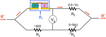
The composition of solder joints used in this study was Sn-based alloy with 2.5 wt% of Ag. The UBM on the cathode side was a trilayered sputtered film of TiW/Cu/Ni. The anode side was a Cu pad with Sn plating surface finish and Sn–2.3Ag stencil printed SOP. The samples were divided into two groups, where one group was subjected to a single solder reflow process during assembly, while the other group was subjected to four additional reflows post-assembly. All reflow processes during assembly and post-assembly followed an industrial standard procedure for Pb-free solders, with a peak temperature of 240 ± 5 °C and a cooling rate of 0.5–2.0 °C/s. A series of accelerated EM tests were performed on a pair of solder joints in each test structure. The EM stressing conditions ranged from 1.39 × 10⁴ to 2.19 × 10⁴ A/cm2, where the current density was calculated based on the UBM opening area. The temperature increase induced by Joule heating was determined using a die metal thermistor. The oven temperature was set such that the actual temperature of the test structures ranged from 150 to 166 °C. To detect damage formation and the time to failure, resistance changes were monitored by the Wheatstone bridge method, which has been discussed elsewhere.Reference Ding11Figure 1 shows the schematic of the Wheatstone bridge setup, where R1 represents the pair of solder joints under test.
An illustration on the Wheatstone bridge method to track resistance change in solder joints during electromigration (EM) tests.

B. Analysis of Sn grain structure
Microstructure characterization was performed at several stages during test: on solder joints prior to EM tests to investigate the effect of solder reflows, on solder joints failed during EM tests to determine failure mechanisms, and on solder joints subjected only to thermal aging to separate the thermal effect from the EM-induced effect. All bumps under investigation were cross-sectioned and examined using the backscattered scanning electron microscopy (BS-SEM) to observe IMC growth and void formation. This was supplemented with an energy dispersed x-ray (EDX) analysis to identify the IMC phase, and finally used the electron backscattering diffraction (EBSD) technique to determine the Sn crystallographic orientation and grain size. The EBSD patterns were obtained in the SEM by focusing the electron beam onto the sample surface at a tilt angle of 70° with respect to the horizontal. Since it is a surface sensitive technique with its diffraction region formed within the top 10–20 nm of the specimen, it is important to have a defect-free sample surface. A final polishing, using 0.05-μm colloidal silica, is required in addition to grinding and polishing steps to assure high-quality EBSD patterns.
In this study, solder joints were investigated using a Zeiss (Thornwood, NJ) Neon40 field emission SEM equipped with an EDAX (Mahwah, NJ) APEX 2 integrated EDS and EBSD system. The scanned data were post analyzed using the EDAX TSL OIMTM 5.0 software.
III. RESULTS AND DISCUSSION
A. Failure analysis of EM-tested solder joints
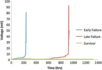
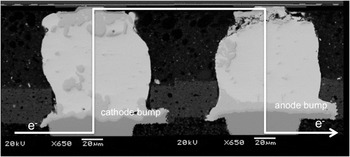
EM tested samples were cross-sectioned and analyzed using SEM. Figure 2 shows Wheatstone bridge voltage (V g) traces as a function of testing time for three test samples, representing early failure, late failure, and survivor. For the first two samples, V g was found to increase first slowly in the initial stage, and then followed by an abrupt jump corresponding to 90–95% opening of the solder joint. The first resistance jump was taken to be failure of the test vehicle. Figure 3 shows the BS-SEM image of a typical pair of solder bumps after the EM test, with arrows indicating the electron flow direction. The anode bump where electrons flowed from the UBM side to the substrate pad suffered from local current crowding, and as it turned out, was the weaker bump that failed first. As shown in Fig. 3, EM damage was found near the UBM side. Although the cathode bump contained a large amount of Cu6Sn5 IMCs accompanied with extensive Cu dissolution, no crack or extended void accumulation was observed. Failure analysis from hereinafter will focus on the anode bumps only.
Change of the voltage across the Wheatstone bridge (V g) versus EM test time of three test vehicles.

Backscattered scanning electron microscopy (BS-SEM) image of a pair of cross-sectioned solder joints after EM testing.

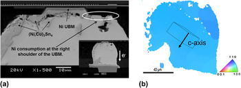
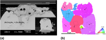
Figure 4 shows the cross section of a solder joint, which was the first to fail among all test samples. The BS-SEM image [Fig. 4(a)] reveals that most of the Ni UBM layer was consumed under the EM test and the open failure occurred at the interface between the IMC and the solder material. (Ni,Cu)3Sn4 IMCs were observed to be swept away from the UBM region to the other side of the solder joint verified by the EDX analysis. Figure 4(b) is the EBSD mapping of Sn, and the legend of the inverse pole figure color is shown as inserted. Figure 4(b) indicated that the solder joint was mono-oriented with a single grain. The angle between the c-axis of the Sn grain and the electron flow direction was calculated using a mathematical relationship between the Euler angle of the crystal orientation (ϕ1, ϕ, ϕ2) and the Cartesian coordinate system transformation matrix g. The value of the angle was found ranging from 0 to 90° characterizing how closely the c-axis of the Sn grain aligns to the electron flow direction. The angle goes to 0° when the c-axis is perfectly parallel with the electron flow direction and conversely goes to 90° when the c-axis is perpendicular to the electron flow direction. This is worth noting that the angle offers a way to verify the significance of the interstitial diffusion of Ni in the Sn matrix contributing to damage formation. In this particular solder joint, for example, the Sn grain was oriented such that its c-axis was aligned 36° off from the current direction, as illustrated in Fig. 4(b). This fact, combined with the BS-SEM image shown in Fig. 4(a), clarifies the role of the Sn grain orientation in affecting the IMC formation during EM tests. First, the IMC did not grow strictly following the current direction; instead, they tended to form at the left side of the solder joint, especially at the lower left corner [Fig. 4(a)], which was exactly along the direction of the c-axis. Second, the right shoulder of the UBM away from the current crowding area suffered a more severe Ni consumption than the left shoulder, which could not be explained unless we considered the grain orientation effect. In other words, the tetragonal cells provided Ni/Cu with an interstitial diffusion path that was much faster than Sn self-diffusion. This suggested that the low-angle alignment facilitating fast IMC growth and Ni depletion, together with the EM-enhanced vacancy transport, caused the early failure of the solder joint under current stressing.
Cross-sectional analysis of an early failed solder joint, which failed after 237 h of current stressing. Test condition: 5.57 × 10⁴A/cm2, 158 °C. (a) BS-SEM image and (b) Electron backscattering diffraction (EBSD) inverse pole image of the Sn grain with c-axis alignment illustration.

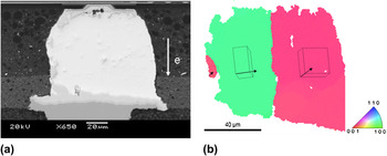
Figure 5 shows the case of a late failure. The black holes inside the IMCs were not due to EM damage; they were particles embedded during polishing. It was found from the BS-SEM image [Fig. 5(a)] that although Ni dissolution led to extensive IMC growth in the forms of (Cu,Ni)6Sn5 and (Ni,Cu)3Sn4, IMCs were limited near the UBM region rather than spreading out elsewhere in the solder joint. This implied a mechanism that helped slow down the diffusion process of the fast diffusion species and block Ni from further depletion. We attributed this EM degradation mechanism to the specific Sn grain structure as shown in Fig. 5(b). The EBSD mapping revealed a multigrain structure with various grain orientations. In this case, we were particularly interested in the crystallographic orientations of grains adjacent to the UBM region where IMC formed. The angles between the c-axis of the three top grains and the current direction were found to be 58, 89, and 59°, respectively. Thus, the grain orientations displayed a relatively high angle against the current direction compared to that of the early failure. The fast interstitial diffusion path was therefore cut off by both moderately high-angle alignment and multigrain structure.
Cross-sectional analysis of a late failed solder joint, which failed after 924 h of current stressing. Test condition: 5.57 × 10⁴A/cm2, 158 °C. (a) BS-SEM image and (b) EBSD inverse pole image of Sn grains with c-axis alignment illustrations.

The solder joint that was even more resistant to the EM test is shown in Fig. 6. It was a survivor that did not fail according to the V g trace (Fig. 2) after 1295 h of testing under 1.39 × 10⁴A/cm2 at 158 °C. As revealed in Fig. 6(a), the Ni UBM remained intact, functioning as an excellent electrical contact. A uniform thickness of IMC layer also minimized the volume shrinkage that would increase the stress level at the IMC/solder interface. The EBSD mapping [Fig. 6(b)] shows that the solder joint was composed of three grains, with their c-axes aligned 80, 83, and 80°, respectively, to the current direction. The high angle almost perpendicular alignment again confirmed a strong correlation between the Sn grain orientation and the EM reliability.
Cross-sectional analysis of a surviving solder joint, which did not fail after 1295 h of current stressing. Test condition: 5.57 × 10⁴A/cm2, 158 °C. (a) BS-SEM image and (b) EBSD inverse pole image of Sn grains with c-axis alignment illustrations.

Failure analyses mentioned above indicate that IMC formation strongly depends on Sn grain orientation in various ways, such as how much, how fast, and where they form. Given the present observation, it would be interesting to find any solution that is able to avoid a single large grain with a low-angle current alignment and instead to produce multiple grains with a high-angle current alignment. For this purpose, we subjected the solder joints to different thermal processes and carried out further EBSD analyses. Since the solder microstructure is highly influenced by the solidification conditions, we expected that the grain structure can be modified by changing the solder reflow profile, such as number of reflows, the cooling rate, and the temperature range. Thus, we investigated the effect of multiple solder reflows and the study was supplemented by an investigation on microstructural evolution under thermal aging, which might contribute to EM degradation of the solder joints.
B. Effect of multiple reflows
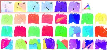
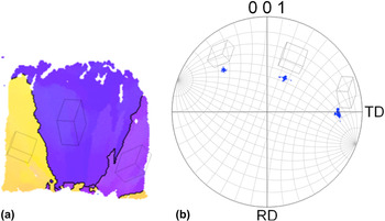
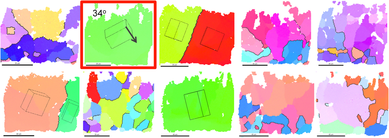
To investigate the effect of multiple reflows on the Sn grain structure, 30 as-received solder joints prior to EM stressing were randomly sampled from each of the single- and multiple-reflow groups. These solder joints were cross-sectioned and characterized using the EBSD technique. Figure 7 is an overview of EBSD mappings of solder joints subjected to a single solder reflow process during assembly. The tetragonal frames at each grain location illustrate grain orientations. After a standard reflow process during assembly, the Sn–2.5Ag solder joints had only a few large Sn grains per bump. In fact, most of them had only one large grain clearly shown in the first three rows of the figure. Moreover, a significant portion of the bumps exhibited a low-angle c-axis alignment to the current flow direction, as presented in the first row of the figure. The numbers in the figure indicate the angles between the c-axis and the electron flow direction. Solder joints with a few large grains are shown in the last row in Fig. 7, where only two to three grain orientations are observed. Grain boundaries with a 60° rotation about the (301) plane and the <100> axis within a tolerance value of 5° were highlighted in black solid lines as shown in Fig. 7. It is interesting to note that such grain boundaries satisfied the β-Sn’s twin misorientation relationship, which is in good agreement with previous observations in large Sn–Ag solder balls.Reference Seo, Kang, Shih and Lee10 The cyclic twin structures are further illustrated in Fig. 8. With the (001) pole figure projected on a Wulff net, the 60° rotational relationship is clearly demonstrated.
EBSD mappings of pristine solder joints subjected to a single solder reflow process.

Cyclic twin structures appeared in solder joints subjected to a single solder reflow during assembly: (a) EBSD mapping and (b) (001) pole figure projected on the Wulff net.

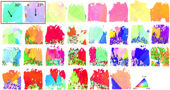
Figure 9 presents the EBSD mappings of 30 solder joints subjected to four additional reflows post-assembly. It was found that grains with smaller sizes were nucleated after multiple reflows. Interestingly, the fine grain structures had a tendency to accumulate at the bottom of the solder joints near the substrate pad side. Only a small fraction of the solder joints had grain structures with a single Sn grain and a low-angle c-axis alignment; instead, multigrain structures were mostly observed. In fact, only 2 out of 30 had this issue as shown in the highlighted boxes.
EBSD mappings of pristine solder joints subjected to four additional reflow processes.

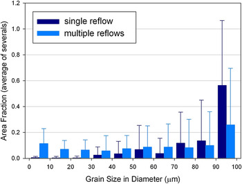
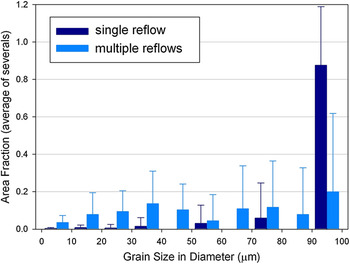
The grain size histogram for groups with and without additional reflows is shown in Fig. 10. The results were an average of grain histograms for 30 cross-sectioned solder joints, where the error bars indicated the standard deviation. The two groups were found to be characterized by different grain size distributions from a statistical point of view. For the single-reflow group, solders tended to form large grains expanding the whole solder bump with an average grain size greater than 60 μm. For solders with multiple reflows, on the other hand, some of the large grains broke down into finer ones, resulting in a more even distribution in grain size.
Grain size histogram for pristine solder joints with single or multiple reflows.

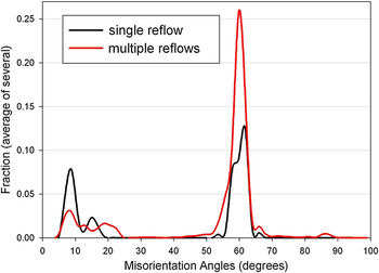
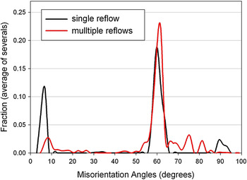
The misorientation histogram for both groups is shown in Fig. 11. The result confirmed that most of the grain boundaries were either small angle boundaries (<20°) or 60° twin boundaries. Moreover, the multiple-reflow group exhibited a smaller fraction of low-angle boundaries and a larger fraction of twin boundaries compared to the single-reflow group. This result, combined with the EBSD mappings, showed that solder joints with a single reflow consisted of cyclic twins, while interlaced twin structures were more commonly observed in solder joints with multiple reflows. Results from Figs. 10 and 11 suggested that both grain size and orientation of solder joints changed after four additional reflows, which will be correlated to its enhanced EM reliability in later discussion.
Misorientation histogram for pristine solder joints with single or multiple reflows.

Previous failure analyses showed that the presence of a single large grain with a low-angle c-axis aligned along the current direction enhanced Ni diffusion, accelerated IMC formation, and increased the statistical probability of early failure. Hence, it is suggested that a single solder reflow process that produced large grains was not favorable for the EM reliability. In contrast, EBSD study indicated that four additional solder reflows resulted in a multigrain structure rendering the diffusion properties of the solder joints less “anisotropic.” This effectively reduced the probability of c-axis alignment with the current flow, and thus minimized the risk of early failure.
C. Effect of thermal aging
At this point, it becomes necessary to investigate the effect of thermal aging on the Sn grain evolution since the EM test temperature may yield the grain structures different from the pristine unstressed ones. Grain structures of solder joints were investigated after isothermal treatment at 150 °C for 450 h. For each group, 10 solder joints were randomly chosen, cross-sectioned, and scanned for EBSD mapping, as shown in Figs. 12 and 13. Twin boundaries were highlighted in dark solid lines. While the group with single reflow (Fig. 12) showed single large grains dominating the grain structure, the group with four additional reflows (Fig. 13) revealed that the majority of the solder joints were composed of multiple grains. The small interlaced twins were observed for solder joints after multiple reflows as shown in Fig. 9, but they tended to grow larger when subjected to thermal aging, as can be seen in Fig. 13. The transformation indicated that the interlaced twinning structures were not thermodynamically favored and would reach equilibrium through grain growth. The grain growth resulted in a reduction in grain boundary areas. Consequently, the system energy was reduced.
EBSD mappings of solder joints after 450 h of thermal annealing under 150 °C. Solder joints were from the group of single reflow.

EBSD mappings of solder joints after 450 h of thermal annealing under 150 °C. Solder joints were from the group of multiple reflows.

Similar quantitative methods as in Figs. 10 and 11 were used to the microstructural characterization, with the results shown in Figs. 14 and 15. Figure 14 shows the grain size histogram averaged over 10 solder joints for each group. Both groups exhibited some limited grain growth after thermal aging. In case of solders with a single reflow, the average grain size exceeded 80 μm, whereas for the multiple-reflow group, grains smaller than 10 μm were coarsened into larger grains. The misorientation histogram for solder joints subjected to only thermal aging is shown in Fig. 15. Compared to the results of pristine unstressed bumps in Fig. 11, fractions of low angle and 60° twinning peaks increased in solder joints in the group of single reflow. The observation indicated that primary grain growth occurred in single-reflowed solder joints during thermal aging, and this grain growth favors the interfacial energy of special boundaries, i.e., low angle and 60° twinning. On the other hand, during subsequent reflows, interlaced twins with much smaller sizes were nucleated. The grain growth of the interlaced twins exhibited a different mechanism that had a preferred interfacial energy of high angle (70–80°) as well as low angle and 60° twinning. Consequently, the Sn grain orientations showed more diversity in the group of multiple reflows as shown in Fig. 15. This effectively made individual solder joints more “isotropic.”
Grain size histogram for solder joints after 450 h of thermal annealing under 150 °C. Groups with single or multiple reflows were compared.

Misorientation histogram for solder joints after 450 h of thermal annealing under 150 °C. Groups with single or multiple reflows were compared.

D. Effects of Sn grain structure on the EM lifetime and statistics
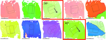
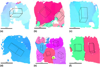
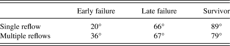
The EM test results were combined with the microstructural characterization to study the effects of Sn grain structure on EM lifetime and statistics. Figure 16 shows a collection of the EBSD mappings for EM-tested solder joints subjected to a single or multiple solder reflows. An early failure, a late failure, and a survivor from each group were shown to illustrate how EM lifetime was affected by Sn grain structure. It was found from Figs. 16(a) and 16(d) that solder joints with single grain structures have a higher risk of early failure under EM than multigrain structures. When the c-axis of the single grain is aligned closely to the current direction, atoms such as Ni and Cu can diffuse interstitially in the Sn matrix along its c-axis with a fast rate. This fast anisotropic diffusion leads to significant depletion of the UBM material in a short time and the eventual open failures. In contrast, multigrains with 60° twin boundaries effectively averaged out the anisotropic properties in the solder joints, and therefore were effective in retarding early failures, which was confirmed by Figs. 16(b) and 16(e). Furthermore, as shown in Figs. 16(c) and 16(f), the grain orientation with the c-axis alignment normal to the current direction led to a longer EM lifetime. It was clear that both Sn grain size and orientation could contribute to the IMC growth and void formation and impact EM reliability of Sn-based Pb-free solders. To better illustrate the combined effect of grain size and orientation, Table I gives the results of angles between the c-axis of the Sn grains and the EM flow direction based on an area weighted average calculation for solder joints shown in Fig. 16. For multigrain structures, the averaged angle with respect to the EM flow direction was obtained by summing up the individual grain orientations weighted by their grain sizes. Again, a good correlation between the grain structure and the EM lifetime was observed.
A collection of EBSD mappings of EM tested solder joints. (a)–(c) were solder joints from the group of single reflow, while (d)–(f) were solder joints subjected to multiple reflows. (a, d) Early failures, (b, e) late failures, and (c, f) survivors.

Results of angles between the c-axis of the Sn grain and the electromigration flow direction based on an area weighted average calculation for solder joints shown in Fig. 16.
The statistical distributions in the EM lifetime for groups with and without additional reflows are shown in Fig. 17. The experimental matrix along with EM statistics was summarized in Table II. The single-reflow group had a standard deviation, σ, larger than that of the multiple-reflow group, which was consistent with the Sn grain characteristics. A small standard deviation is desired when we obtain the EM lifetime under operating temperature by extrapolating the experimental data under testing temperature. Multiple solder reflow processes enabled a more homogeneous Sn microstructure from one joint to another with a small standard deviation, thus effectively improved the EM statistics.
Statistical distribution for EM lifetime for solder joints with and without four additional reflows.

Summary of the experimental matrix and electromigration statistical results.

E. Discussion
These experimental observations offer new understanding and practical implications in the EM reliability of Sn-based Pb-free flip chip solder joints, which will be discussed as follows.
First, given the fact that flip chip solder joints fall in the category of limited supply of UBM and ample supply of Sn-based solder material, two critical factors would affect the EM reliability, i.e., IMC formation and the microstructure of Sn. The wetting of the UBM accompanies the creation of an interface between the IMC and the solder material. This interface acts as a vacancy source in that atomic diffusion in different materials results in a flux divergence at the interface, which makes it vulnerable for damage formation under EM stressing. The thin UBM is gradually consumed and dissolved into the solder joint under a rate that is dependent on the Sn grain orientation, rendering the microstructure and anisotropic property of Sn an important role in controlling the EM damage formation. In the present study, the Sn grain orientation has been closely correlated to the EM lifetime and statistics for Sn-based Pb-free solders where Sn remains the predominant phase in the system throughout the EM test.
Second, it has been demonstrated that either single grain with c-axis parallel to the substrate or multigrain structure with random c-axis orientations promotes the solder resistance to EM. Here, only the EM reliability is taken into account. However, it has been shown by other research groupsReference Bieler, Lehman, Kirkpatrick, Cotts and Nandagopal8 that grains with c-axis perpendicular to the substrate is preferable in terms of its thermomechanical reliability such as fatigue resistance, since cracks are less likely to occur when the c-axis is aligned in this way. In other words, the anisotropic behavior of Sn leads to opposite conclusions for EM and mechanical reliabilities. This makes it difficult to optimize the Sn solder with a single grain or a few large grains simply by controlling the grain orientation since promoting the one aspect would sacrifice the other. Furthermore, it is difficult to control the crystal orientation using the standard industrial process. Alternatively, producing multigrain structures in solder joints resulting from multiple reflows is a practical approach to benefit from a longer EM lifetime with a tighter statistics, which at the same time would not degrade mechanical properties.
Third, our study has shown that multiple solder reflow process is an effective approach to achieve multigrain structures in solder joints. This can probably attribute to the fact that the β-Sn phase is difficult to nucleate from the liquid, which results in a large amount of undercooling during solidification. Indeed, a considerable degree of undercooling of 40–80 °C has been reported in Pb-free flip chip solder joints, inversely increasing with decreasing sample size. Other metallurgy parameters can also affect the microstructure of solder joints during the solidification process, including the solder alloy composition, minor alloying elements, UBM, impurity level of Sn, cooling rate, and holding time.Reference Kang, Cho, Lauro and Shih12 Considering a few individual grains observed in solder joints after a single-reflow process, it is possible that only a few nuclei are required to initiate solidification for a solder joint of a hundred micrometer in diameter. Due to the great amount of undercooling, rapid solidification occurs in the molten solder alloy once one or two nucleation sites are formed, which would produce solder joints with large grains and anisotropic properties. The addition of solder reflow process, in this case, dissolves Ni (on the UBM side) and Cu (on the substrate side) atoms into the solder joint. The more times the solder joints are reflowed, the greater amounts the Ni and Cu dissolve. The change in solder composition after multiple solder reflows would reduce the undercooling of β-Sn during solidification. This is consistent with other studiesReference Anderson and Harringa13 reporting that undercooling can be effectively reduced due to a small addition of Ni. Hence, solder joints solidified with less undercooling are more likely to exhibit finer grain structures with interlaced twin boundaries, rendering a more isotropic material property. Based on our results, while standard multiple reflow can be a promising way to produce multigrain structures, single grain structures cannot be completely avoided. The observation showed the random nature of the nucleation event. Further investigation on joining integrity to improve the process consistency is therefore suggested.
Lastly, we have studied the effect of multiple reflows by using solder joints subjected to four additional reflow processes post-assembly. Further research is required to better understand the microstructural evolution as a function of times of reflow. This is of practical importance in the industry when evaluating solder joint reliabilities in ball grid array packages versus land grid array packages.
IV. CONCLUSIONS
Sn grain structures were characterized using the EBSD technique to investigate the effect of multiple reflows and thermal aging. The material characterization was correlated to the EM reliability of Sn–2.5Ag (wt%) flip chip solder joints. From this study, we have drawn the following conclusions:
(i) A single solder reflow during assembly produced solder joints with the majority of Sn grains with a large grain size and a random spread of grain orientations. Thermal aging caused further grain coarsening.
(ii) Four additional post-assembly reflows yielded solder joints with smaller grain sizes. More 60° interlaced twin boundaries were also observed. Thermal aging caused some grain growth, while the multigrain feature remained.
(iii) EM failure mode was closely related to the alignment between the c-axis of the Sn crystal and the current flow direction. Single large grain may lead to EM early failure when its c-axis aligns to the current flow direction.
(iv) Optimization of Sn grain structures to produce multigrains with high-angle twin boundaries is an effective approach to improve EM lifetime and statistics.
ACKNOWLEDGMENTS
The authors thank Karen Robinson, Joe Garcia, and William Buniak of Dallas Flip Chip Assembly, Texas Instruments, Inc., for help with sample preparation. The work was funded by the Semiconductor Research Corporation.