While working at the Molecular Physics Laboratory at SRI International in 1991, I noted an article by Iijima in Nature on carbon nanotubes.Reference Iijima1 Considering graphite (three-dimensional) along with this article on carbon nanotubes (one-dimensional), I started thinking: Why not large two-dimensional sheets of sp 2-bonded carbon (now referred to as graphene)? One could expect such a material to have exceptional mechanical, thermal, and possibly electronic properties, from the well-known in-plane properties of graphite. However, my search of the literature did not find any examples of scalable methods of exfoliating graphite based on liquid-phase processing, although there were some tantalizing discussions of achieving enormous expansion in the interlayer spacing of other layered materials such as vermiculiteReference Walker and Garret2 and montmorilloniteReference Norrish3 in the early literature. Eventually, the expansion can reach a point where the layers are so far apart from each other that crystal integrity is lost and the gentlest agitation of the liquid leads to complete exfoliation. Indeed, vermiculite, a phyllosilicate layered material similar to mica in structure, is exfoliated on a very large scale, and the thin layers obtained are used in many applications, including as an additive to cement.4
To date, liquid-phase processing methods for converting graphite to pristine graphene platelets that are scalable to tens or millions of tons have not been reported. Meeting this challenge would provide such graphene “flake” material for a host of important applications, for example, conductive inks; filler for polymer, rubber, ceramic, and possibly metal composites; electrode material for electrical energy storage in ultracapacitors and batteries; conductive thin films; barrier films; and many others.
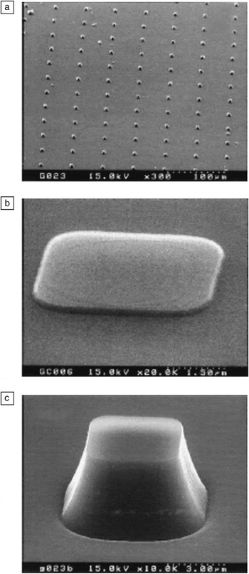
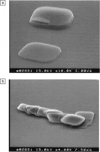
After moving to the Physics Department at Washington University in 1996, I conceived of a method to achieve individual layers of graphite (i.e., graphene, as defined by the International Union of Pure and Applied Chemistry in a 1995 publicationReference Fitzer, Kochling, Boehm and Marsh5) of controlled shape and lateral dimensions, through top-down lithographic patterning of graphite, such as from high-quality samples of highly oriented pyrolytic graphite (HOPG).Reference Lu, Huang, Nemchuk and Ruoff6, Reference Lu, Yu, Huang and Ruoff7Figure 1 shows the patterned pillars obtained using this process, and Figure 2 shows what happened when the pillars were rubbed with a piece of silicon wafer, as observed by scanning electron microscopy. Quoting from Reference Reference Lu, Yu, Huang and Ruoff7:
Scanning electron microscopy (SEM) images of graphite pillars created by oxygen plasma etching on a highly oriented pyrolytic graphite substrate. The scale markers in the border at the bottom right of each image denote (a) 100 μm, (b) 1.50 μm, and (c) 3.00 μm. Reproduced with permission from Reference Reference Lu, Yu, Huang and Ruoff7. ©1999, IOP Publishing.

SEM images of multilayer graphene platelets transferred by rubbing onto a Si(001) substrate. The scale markers in the border at the bottom right of each image denote (a) 3.00 μm and (b) 7.50 μm. Reproduced with permission from Reference Reference Lu, Yu, Huang and Ruoff7. ©1999, IOP Publishing.

Since graphite can be easily cleaved along the basal plane, the islands can be transferred to flat surfaces of other substrates, such as mica or Si, simply by rubbing the HOPG surface against the surface of other substrates. Figure 2 shows islands transferred onto a Si(001) substrate. The original islands were 6 μm in height. After being transferred to a Si(001) substrate, all the islands were “fanned out” into smaller-height pieces. Well-separated as well as stacked plates were found on the surface, as shown in Figure 2. It was noticed that some very thin plates were created by this method of transferring from the patterned HOPG surface onto the Si surface. This implies that more extensive rubbing of the patterned (island) HOPG surface against other flat surfaces might be a way to get multiple or even single atomic layers of graphite plates.
This approach was subsequently used in other attempts at micromechanical exfoliation, including “rubbing” the pillars with a truncated atomic force microscope tip to cleave multilayer plateletsReference Zhang, Small, Pontius and Kim8 and in the now-famous “Scotch-tape” approach that generated monolayer graphene flakes.Reference Novoselov, Geim, Morosov, Jiang, Zhang, Dubonos, Grigorieva and Firsov9
To further explore the idea of exfoliation of controlled-geometry graphene, I formed a collaboration with electrochemist/inorganic chemist Michael Lerner of Oregon State University in 1998–1999. Specifically, we used large intercalants [such as bis(trifluoromethanesulfonyl)imide and other anions with perfluoroalkanesulfonyl substituents] that he and his group had already found could intercalate into large graphite pieces,Reference Zhang and Lerner10–Reference Zhang and Lerner13 greatly expanding the adjacent layers. I thought that the large interlayer separations that his team had achieved in larger graphite pieces would make obtaining individual layers from smaller areas in patterned pillars “straightforward.” Our team was surprised to find that the pillars did not intercalate, and we also did not understand why they did not. (For this reason and also because intercalation is, in principle, a promising approach, I consider this technique to be worth revisiting for pillars created by such types of lithographic patterning or by methods such as direct cutting.Reference Mohanty, Moore, Xu, Sreeprasad, Nagaraja, Rodriguez and Berry14)
Of the more than 130 articles that I have co-authored on graphene, I next mention a few other ways in which our group (sometimes in collaboration with other groups) has made and studied graphene. In addition to our aforementioned investigations of top-down lithography to create and micromechanically exfoliate layers of graphite,Reference Lu, Huang, Nemchuk and Ruoff6, Reference Lu, Yu, Huang and Ruoff7 our work has included chemically modifying graphene platelets and performing large-area growth of monolayer graphene by chemical vapor deposition (CVD),Reference Stankovich, Dikin, Dommett, Kohlhaas, Zimney, Stach, Piner, Nguyen and Ruoff15–36 as discussed next.
Pioneering studies in the use of chemically modified graphene platelets included using them as a conductive filler to make electrically conductive polymer composites,Reference Stankovich, Dikin, Dommett, Kohlhaas, Zimney, Stach, Piner, Nguyen and Ruoff15 overlaying them and thereby forming thin films and mechanically strong “paperlike” films,Reference Dikin, Stankovich, Zimney, Piner, Dommett, Evmenenko, Nguyen and Ruoff16 embedding them in silica to make optically transparent electrically conductive films,Reference Watcharotone, Dikin, Stankovich, Piner, Jung, Dommett, Evmenenko, Wu, Chen, Liu, Nguyen and Ruoff17 developing simple optical methods for imaging them at high contrast,Reference Jung, Pelton, Piner, Dikin, Stankovich, Watcharotone, Hausner and Ruoff18 and synthesizing 13C-labeled graphite and thus 13C-labeled graphite oxide and studying its structure with solid-state nuclear magnetic resonance spectroscopy.Reference Cai, Piner, Stadermann, Park, Shaibat, Ishii, Yang, Velamakanni, An, Stoller, An, Chen and Ruoff19 In addition, we tuned the electrical conductivity of individual platelets of graphene oxide by thermal reduction,Reference Jung, Dikin, Piner and Ruoff20 mapped their solubility behavior using solubility parameters,Reference Park, An, Jung, Piner, An, Li, Velamakanni and Ruoff21 and used them as the electrode material in supercapacitor (ultracapacitor) devices.Reference Stoller, Park, Zhu, An and Ruoff22 We also discovered a graphene-derived material called activated microwave-expanded graphite oxide (a-MEGO), achieving significantly improved performance in terms of energy densityReference Zhu, Murali, Stoller, Ganesh, Cai, Ferreira, Pirkle, Wallace, Cychosz, Thommes, Su, Stach and Ruoff23 and high-frequency responseReference Zhang, Zhao, Stoller, Zhu, Ji, Murali, Wu, Perales, Clevenger and Ruoff24 for electric double-layer (EDL) capacitors, as well as excellent performance with a-MEGO used as the cathode in a lithium hybrid battery/supercapacitor device.Reference Stoller, Murali, Quarles, Zhu, Potts, Zhu, Ha and Ruoff25
Regarding the electrical energy storage possibilities of graphene,Reference Stoller, Park, Zhu, An and Ruoff22–Reference Stoller, Murali, Quarles, Zhu, Potts, Zhu, Ha and Ruoff25 note that porous carbons such as activated carbons are used commercially as electrode materials for supercapacitors because of their high specific surface area (on a gravimetric or volumetric basis). This large area translates into a larger stored charge per unit weight or volume, because of more extensive EDL formation over that larger surface. The double layer is formed by the charged carbon attracting oppositely charged ions that are present in the electrolyte, in each half-cell. The high electrical conductivity and surface area of graphene made it a natural choice to test as an electrode material.Reference Stoller, Park, Zhu, An and Ruoff22
We also found that, by activating an expanded graphite oxide material, it is possible to generate a new type of carbon (a-MEGO) having atom-thick walls and surface areas exceeding the theoretical limit of graphene itself (which is 2630 m2/g), namely, as high as 3100 m2/g.Reference Zhu, Murali, Stoller, Ganesh, Cai, Ferreira, Pirkle, Wallace, Cychosz, Thommes, Su, Stach and Ruoff23 Use of chemically modified graphene as a precursor allowed this almost-pure-carbon a-MEGO product to be made (thus, a “graphene-derived” material) that exhibits exceptional performance as a new electrode material.
In another research direction, we discovered a scalable method for the large-area CVD growth of monolayer graphene,Reference Li, Cai, An, Kim, Nah, Yang, Piner, Velamakanni, Jung, Tutuc, Banerjee, Colombo and Ruoff26 used Raman mapping of isotopically labeled graphene films to understand growth mechanisms,Reference Li, Cai, Colombo and Ruoff27 studied CVD-grown graphene for transparent conductive film applications,Reference Li, Zhu, Cai, Borysiak, Han, Chen, Piner, Colombo and Ruoff28 enormously increased the grain size from micrometers to millimeters of monolayer graphene,Reference Li, Magnuson, Venugopal, An, Suk, Han, Borysiak, Cai, Velamakanni, Zhu, Fu, Vogel, Voelkl, Colombo and Ruoff29, Reference Li, Magnuson, Venugopal, Tromp, Hannon, Vogel, Colombo and Ruoff30 studied the thermal transport of isotopically labeled graphene,Reference Chen, Wu, Mishra, Kang, Zhang, Cho, Cai, Balandin and Ruoff31 showed that graphene acts as an excellent barrier protecting bare metals from oxidation,Reference Chen, Brown, Levendorf, Cai, Ju, Edgeworth, Li, Magnuson, Velamakanni, Piner, Kang, Park and Ruoff32 discovered that graphene and lightly oxidized graphene are superb supports for transmission electron microscopy imaging of biological molecules,Reference Pantelic, Suk, Magnuson, Meyer, Wachsmuth, Kaiser, Ruoff and Stahlberg33, Reference Pantelic, Suk, Hao, Ruoff and Stahlberg34 and explained how chemical functionalization in selected regions could be used to make new devices.Reference Ruoff35 Other studies are listed on the publications page of our research group web site.36
In one of these discoveries, the thermal conductivity of 99.99% 12C-pure graphene was found to be significantly higher than that of normal graphene (that is, 98.9% 12C and 1.1% 13C) at room temperature: about 4700 W m–1 K–1 versus about 2800 W m–1 K–1.Reference Chen, Wu, Mishra, Kang, Zhang, Cho, Cai, Balandin and Ruoff31 This dramatic difference is due to phonon–isotope scattering , and it is likely that the difference at lower temperatures will be much larger. Could isotopically pure graphene be used for thermal management? If the answer depends only on cost (because it looks favorable in all other aspects), then cost is, perhaps surprisingly, not a strong factor, as 12C-pure graphene can be made in square-meter (or larger) sizes for relatively low cost.
We now turn to an earlier history of experimental work on graphene. It seems that the (experimental) discovery of graphene is (ironically) due to a theoretician, namely, John May,Reference May37 who published in 1969 a complete analysis of unassigned low-energy electron diffraction (LEED) data published by the Somorjai group in 1965–1968.Reference Hagstrom, Lyon and Somorjai38–Reference Morgan and Somorjai41 These LEED data had been obtained by exposing single-crystal metal substrates to hydrocarbons at elevated temperatures, experiments undertaken because poisoning of such metals in industrial catalyst beds by hydrocarbons was a problem and the mechanism of poisoning was not understood. May assigned those publishedReference Hagstrom, Lyon and Somorjai38–Reference Morgan and Somorjai41 LEED patterns to “monolayer graphite” attached to the single-crystal substrate surface, and he also assigned other sets of published LEED patterns to stacked layers, including with neighboring graphene layers misoriented with respect to AB (Bernal-type) stacking.
Given the current intense interest in achieving control of the stacking orientation of multiple layers, May’s solving of the structure of misoriented multilayer graphene samples in 1969Reference May37 is a sort of “back to the future” success. Controlling interlayer registry is a challenge whose successful achievement will probably also influence the realization of sp 3 and sp 2–sp 3 hybrid materials that might be derived from graphene, as discussed next. (Electronic transport measurements of AB- and non-AB-stacked CVD-grown bilayer graphene have recently been presented and described.Reference Fallahazad, Hao, Lee, Kim, Ruoff and Tutuc42)
I recently presented a Perspective in Nature on graphene as a precursor for new materials.Reference Ruoff43 Here, I expand on this topic to discuss, for example, one possible (but unproven) pathway to revolutionize quantum computing. As mentioned in my Perspective,Reference Ruoff43 one can consider monolayer graphene as a template from which to build, through clever chemistry, ultrathin “diamond” sheets. (These might be better called something like “ultrathin sp 3-bonded sheets,” as their electronic, optical, and perhaps thermal properties might strongly differ from those of bulk diamond.) In addition to building such sheets from monolayer graphene, computational studies have suggested that bilayer graphene, when functionalized in certain ways on its top and bottom surfaces, could “collapse” into an sp 3-bonded layer and reported some of the calculated physical properties of such ultrathin sp 3-bonded layers.Reference Chernozatonskii, Sorokin, Kvashnin and Kvashnin44–Reference Chernozatonskii, Mavrin and Sorokin48 Therefore, graphene should be considered as a precursor to yield new sp 2–sp 3 hybrid or pure sp 3materials with exceptional properties and applications.
As our team is now using CVD on copper foils to grow graphene with 3–4-mm grain sizes, graphene with centimeter or larger grain sizes might soon be available. With such a material as a template, sp 3-bonded sheets with nanometer thicknesses and large grain sizes could conceivably be made. The bandgap of such thin sp 3-bonded sheets has been calculated to be significantly smaller than that of bulk diamondReference Chernozatonskii, Sorokin, Kvashnin and Kvashnin44–Reference Chernozatonskii, Mavrin and Sorokin48 and could perhaps be shifted by surface functionalization and/or adsorbates, as has been done with graphene. The ability to control thickness down to about the nanometer scale through fine control over the spatial distribution of certain sorts of dopant atoms would yield a variety of doped “ultrathin diamond” films having exceptional mechanical, thermal, and electrical properties. One example would be the incorporation of nitrogen–vacancy (N–V) centers in such sp 3-bonded sheets through substitution of nitrogen atoms in the carbon lattice. Indeed, N–V centers can be used to configure qubits for use in a quantum computer, and it seems to me that this class of thin sp 3-bonded sheets of material could advance that technology. The N–V center in diamond and its potential for quantum computing is reviewed in Reference Reference Weber, Koehl, Varley, Janotti, Buckley, Van de Walle and Awschalom49.
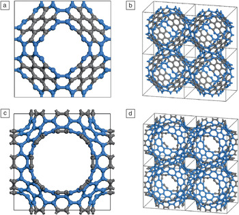
Another class of carbon materials that are reminiscent of graphene but have not yet been made are “negative-curvature” carbons (NCCs), which, when periodic, are beautiful crystal structures with atom-thick walls composed of trivalently bonded carbon. The presence of n-gons larger than hexagons (heptagons, octagons, etc.) introduces Gaussian curvature equal to –1, and to date, these types of carbons have been studied primarily by theory.Reference Townsend, Lenosky, Muller, Nichols and Elser50–Reference Terrones and Terrones56 Several examples are shown in Figure 3. If such structures can be made in large sheets such that the entire sheet is a continuous covalently connected solid, they could serve as an almost ideal electrode material for EDL capacitors with exceptionally fast time responses and energy density values rivaling or exceeding those of lead acid batteries.
Two different negatively curved graphite structures, also known as schwarzites: (a) cubic cell of the schwarzite P8bal surface with 192 carbon atoms, (b) four cubic cells of the structure in (a), (c) cubic cell of the schwarzite P7par surface with 216 carbon atoms, (d) four cubic cells of the structure in (c). Rings larger than hexagons are colored blue in the structures. Prepared by E.S. Paek and G.S. Hwang based on Reference Reference Terrones and Terrones56.

To understand this claim, the reader should consider reading Reference Reference Zhu, Murali, Stoller, Ganesh, Cai, Ferreira, Pirkle, Wallace, Cychosz, Thommes, Su, Stach and Ruoff23 in detail, which describes a form of carbon with an exceptionally high specific surface area (3100 m2/g) and with atom-thick walls of sp 2-bonded carbon. Note that this new carbon material is not a continuously bonded sheet of material; rather, it is a powder made up of many particles. Particle–particle resistance is a problem in electrode materials in current ultracapacitors, and elimination of interparticle resistance by having a “totally connected” network of trivalently bonded carbon in large-area sheet form is thus an important goal. NCCs in the form of such large sheets might also be excellent electrode materials for lithium-ion and other types of batteries.
These NCC materials have other interesting calculated attributes, including unusual mechanics;Reference Park, Kittimanapun, Ahn, Kown and Tomanek53 the possibility of an all-carbon ferromagnet;Reference Park, Yoon, Berber, Ihm, Osawa and Tomanek54 and bandgaps that vary from essentially zero (i.e., metallic) to insulating, depending on the particular NCC modeled.Reference Huang, Ching and Lenofsky55 An infinite variety of these NCC structures are, in principle, available as crystals, and they can also be aperiodicReference Townsend, Lenosky, Muller, Nichols and Elser50 and ought to perform well in many applications in addition to electrical energy storage, for example, as absorbent materials and as catalyst supports with very high surface areas.
Conclusions
Graphene is now the center of worldwide research efforts. This article presented a brief perspective on the history of the discovery of graphene, including efforts by the author and his team (and collaborators) to make and study graphene and chemically modified graphenes by various methods. Several types of carbon materials that have not yet been realized experimentally were also discussed, including large-area ultrathin sp 3-bonded carbon sheets and negative-curvature carbons, as well as some reasons why these materials seem exceptionally promising.
Acknowledgments
It has been my pleasure to collaborate with a number of talented senior scientists and engineers (and in many cases also with their group members) on chemically modified graphene or CVD-grown graphene and of course to have collaborated with the many graduate and undergraduate students and postdoctoral fellows in my group. Specifically for this article, I appreciate Kevin McCarty for pointing out the work of John May and A.L. Ruoff and L. Colombo for critically reading the manuscript. Funding support from NSF, ONR, SWAN-NRI, DOE, DARPA, ARO, AFOSR DURIP, Goodyear, ARPA-E, and the W.M. Keck Foundation has been and is appreciated.