Introduction
Device platforms can be radically transformed by introducing new materials at a fundamental level. Microfluidic devices, for example, were initially constructed from glass and silicon.Reference Whitesides 1 With advances in fabrication techniques, devices constructed on thin polymer substrates emerged and expanded the landscape of potential applications by decreasing the cost and simplifying the materials and equipment required to fabricate microfluidic devices.Reference Whitesides 1 Similarly, in the last decade, microelectronics has experienced a fundamental materials expansion from expensive rigid substrates to now low-cost flexible materials.Reference Rogers, Someya and Huang 2 – Reference Kim, Kim, Wu, Liu, Song, Kim, Hauan, Hwang and Rogers 4 Paper is the latest material to transform the device landscape. Despite the fact that paper was developed nearly 2,000 years ago and has been broadly used in scientific applications, including chromatography, for over 100 years,Reference Tswett 5 new and important uses for this intriguing material are still emerging.
From a materials perspective, paper offers a number of useful attributes: (1) It is low in cost and ubiquitously available in a variety of forms; (2) it has the ability to wick fluids via capillary action; (3) it has a very high surface area due to its microfiber composition; (4) it has the capacity for filtration and separation of microscopic components, such as cells; (5) it is amenable to a wide range of printing technologies; (6) it is an ideal medium for dry chemical storage; (7) it demonstrates very strong adhesion to a variety of materials; (8) it can have high reflectivity and can be easily dyed; (9) it can be cut using a number of low-cost tools and standard techniques; and (10) it can be stacked/folded to generate 3D structures.
Cost is a particularly important consideration, as devices are being developed for new market sectors (e.g., diagnostics, packaging), including 80% of the world that lives on less than $10 per day. This population, approximately 5 billion people, comprises an underserved (and largely untapped) market with great potential.Reference Whitesides 6 By re-engineering complex devices, particularly from a materials point of view, advances in health care, energy, communications, and electronics are poised to have a global impact. The ability to provide reliable medical information on the spot at very low cost may shift the paradigm away from centralized labs, which can delay results and subsequent treatment by weeks in developing nations. Advances in telecommunications—an industry that has successfully accessed developing world markets—integrated with novel low-cost diagnostic platforms, offer a completely new approach to practicing health care across the globe.Reference Martinez, Phillips, Carrilho, Thomas, Sindi and Whitesides 7
Diagnostic devices based on paper in the form of lateral flow tests (e.g., home pregnancy tests) have existed for decades.Reference Posthuma-Trumpie, Korf and van Amerongen 8 Lateral flow has proven to be a useful platform for a large number of immunoassays. The field of paper microfluidics stands to build substantially upon the form and function of lateral flow devices. The ability to pattern paper allows for a degree of fluid control not previously demonstrated. Fluidic operations such as splitting,Reference Martinez, Phillips and Whitesides 9 mixing,Reference Osborn, Lutz, Fu, Kauffman, Stevens and Yager 10 , Reference Rezk, Qi, Friend, Li and Yeo 11 filtration,Reference Pollock, Rolland, Kumar, Beattie, Jain, Noubary, Wong and Pohlmann 12 separations, and even programmed delaysReference Noh and Phillips 13 , Reference Fu, Lutz, Kauffman and Yager 14 are now possible and have prompted the development of paper-based devices capable of high levels of multiplexing,Reference Martinez, Phillips and Whitesides 9 greater sensitivities and specificities,Reference Fu, Kauffman, Lutz and Yager 15 and greater assay diversity.
Finally, paper is ubiquitous in printed media. Over the last several decades, advancements in new materials, printing technologies, paper manufacturing, and nanoscale coatings have dramatically improved print quality and spawned a rising industry in printed electronics.Reference Tobjörk and Österbacka 16 Leveraging the print industry, electronic devices integrated directly into products such as food and pharmaceutical packaging provide new opportunities in advertising, brand enhancement, security, and regulatory compliance. Interactions between paper structure, performance of novel materials, and low-cost sensors are now being widely investigated.Reference Xiang and Lu 17 – Reference Yu and White 21 The integration of these novel devices can allow for useful products such as quantitative assays directly integrated with low-cost sensors.
The base materials properties and technology opportunities for paper devices offer a broad range of research areas. This article will first highlight methods for patterning paper ranging from direct printing of wax barriers to cutting and stacking. This is followed by a look at methods for moving and controlling fluids on paper—a fundamental building block for low-cost microfluidic systems. The article concludes with a brief description of electronics on paper and how these developments are now starting to be combined into fully integrated commercial systems.
Methods of patterning paper
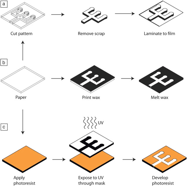
As mentioned previously, paper has the attractive characteristic that it can wick fluids via capillary action. Therefore, unlike open channel microfluidic devices, fluidic devices made from paper have a distinct advantage in that no external pumps, tubes, etc. are required to move a fluid within the device. However, patterning processes are required to create fluidic pathways where wicking is accomplished in a programmed manner. Figure 1 illustrates three such methods for patterning paper (as well as other thin porous materials such as nitrocellulose and nylon membranes). One method (shown in Figure 1c), photolithography, first reported by Whitesides et al.,Reference Martinez, Phillips, Butte and Whitesides 22 involves first saturating a sheet of paper in a photoresist, which is a photosensitive, hydrophobic polymer resin. After the resin is dried, a patterned mask is generated, and the sheet is exposed to UV light through the mask, cross-linking a selective portion of the resin in the sheet. The uncross-linked portion is then washed away using a solvent, and the now patterned paper is dried. This photolithographic technique produces features with very clean edges and with a resolution approaching 100 microns. Additionally, the resulting channels are not prone to leakage and are resistant to a variety of solvents. The method is somewhat laborious, compared to the wax printing technique described later, and requires removal of polymer resin that can lead to residual contamination of the paper channels.
Examples of patterning techniques used to generate paper-based microfluidic devices. (a) Cutting using a knife plotter and adhering to a laminate film;Reference Osborn, Lutz, Fu, Kauffman, Stevens and Yager 10 (b) wax printing;Reference Carrilho, Martinez and Whitesides 23 and (c) patterning using photoresist and masked UV exposure.Reference Martinez, Phillips, Carrilho, Thomas, Sindi and Whitesides 7

Another method, also developed by Whitesides et al., is wax printing (Figure 1b).Reference Carrilho, Martinez and Whitesides 23 This technique makes use of a commercial wax printer, such as the ColorQube manufactured by Xerox, which rapidly deposits wax on the surface of paper. The sheet is then heated above the melting temperature of the wax to allow the wax pattern to permeate through the thickness of the paper sheet while maintaining the original pattern. This technique is a simpler one than the photolithographic method in that it only requires the user to design a pattern on the computer, print the pattern, and briefly heat the sheet. The drawbacks of this method are that it has a resolution of 500 microns, and the resulting hydrophobic features have a higher degree of roughness.Reference Carrilho, Martinez and Whitesides 23
Yager et al. developed another method that involves cutting features from paper using a knife plotter (Figure 1a).Reference Osborn, Lutz, Fu, Kauffman, Stevens and Yager 10 This method has the advantage of simplicity from a fabrication perspective; however, it has the disadvantage that the cut features need to be handled and ultimately laminated to a plastic carrier sheet. Other techniques have been described for patterning paper, including hot embossing of paraffin wax,Reference Müller and Clegg 24 inkjet printing of polydimethylsiloxane (PDMS),Reference Bruzewicz, Reches and Whitesides 25 flexographic printing of polymer solutions,Reference Olkkonen, Lehtinen and Erho 26 ink jetting solvent onto polymer-infused paper,Reference Abe, Suzuki and Citterio 27 and using plasma treatment.Reference Noh and Phillips 13 Undoubtedly, new techniques for patterning paper will continue to emerge as the field progresses from the prototype stage to high volume manufacturing.
Fluidic control in paper systems
With a variety of methods to pattern paper established, a number of “second order” techniques to further control fluid behavior have also been developed.
Sample splitting
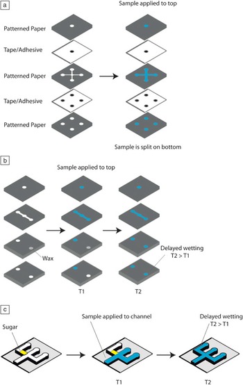
Whitesides et al. demonstrated an elegant sample splitting methodology based on three-dimensional stacking of patterned paper sheetsReference Martinez, Phillips and Whitesides 9 ( Figure 2 a). In this device, a 30 μL droplet can be introduced to the top of the device and sequentially split into hundreds or even thousands of individual zones located on the bottom of the device. This has profound implications for multiplexing assays on paper-based devices. Unlike lateral flow devices, where multiple tests must be run in series (necessitating that each assay on the device be compatible with the others in terms of buffers and other reagents), these 3D devices have the capacity to split a single, low volume sample into multiple separate portions, each of which can be assayed in parallel. This allows for high-level multiplexing of independently optimized assays with distinct assay conditions.
Examples of possible fluidic operations using paper-based microfluidic devices. (a) Sample splitting;Reference Martinez, Phillips and Whitesides 9 , Reference Carrilho, Martinez and Whitesides 23 (b) precision delay of fluid flow using hydrophobic materials;Reference Noh and Phillips 13 and (c) delayed fluid flow using spotted sugar solutions.Reference Fu, Lutz, Kauffman and Yager 14

Sample splitting has also proven useful in 2D devices such as those demonstrated by Garnier et al. for blood typing.Reference Khan, Thouas, Shen, Whyte and Garnier 28 In this case, a lateral three-armed device was able to simultaneously test for all possible blood types from a single whole blood sample.
Dwell time
It is often desirable for a fluid to dwell in a particular region of a device before proceeding to another region. This function has great implications for rate-dependent assays such as immunoassays and enzymatic reactions. It is also useful for the generation of on-chip timers. Phillips et al. reported a novel approach wherein regions of a paper device were made slightly hydrophobic by the addition of paraffin wax into the channelReference Noh and Phillips 13 (Figure 2b). The dwell time could then be precisely controlled by the concentration of paraffin that was deposited. Sophisticated and precise low-cost timers were developed using this technique.
Yager et al. reported the use of sugar solutions spotted onto regions of a device to control the wicking rate along a given channel. The dissolution of the sugar embedded in the paper creates a temporary delay in wickingReference Fu, Lutz, Kauffman and Yager 14 (Figure 2c). Timing of fluid flow was further controlled by simply varying channel dimensions.
Valves
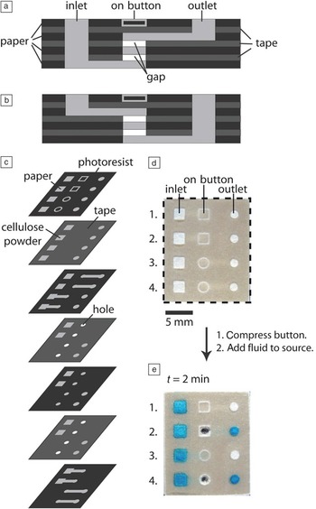
As in the case with open channel microfluidics, valves can play a key role in fluidic operations on paper devices. Unlike open channel microfluidics, valves in paper devices thus far are single use—meaning that they block the wicking of fluid along a channel until activated, at which point flow proceeds irreversibly. Whitesides et al. reported the fabrication of “button valves” that are operated by depressing paper buttons with a ballpoint pen ( Figure 3 ).Reference Martinez, Phillips, Nei, Cheng, Carrilho, Wiley and Whitesides 29 This system allows for a user to pre-select assays before introducing a sample, a function that is useful when sample volume is limited. Shen et al. fabricated single-use valves using sliding regions of paper that block flow in one configuration and permit flow in another.Reference Li, Tian, Nguyen and Shen 30 A similar concept was used to develop multiple paper switches, which can provide timed access to a reactor region for a given assay.
Fabrication of “on” buttons in 3D microfluidic devices. (a) Schematic of the cross-section of an “on” button where the inlet channel is below the outlet channel. The inlet and outlet channels are separated by two gaps and one layer of paper. The location of the button is indicated by a square design patterned on the top of the device. (b) Schematic of the cross-section of an “on” button where the inlet channel is above the outlet channel. (c) Schematic representation of the layers of paper and tape required to assemble a device with four independent “on” buttons. When assembling the device, all the holes in the tape, except those used in the “on” buttons, were filled with cellulose powder. (d) Top of the assembled device with four “on” buttons. Each button has its own inlet and outlet. Buttons 1 and 2 have the inlet channel below the outlet channel, while buttons 3 and 4 have the inlet channel above the outlet channel. (e) Buttons 2 and 4 of the device shown in (d) were compressed, and aqueous blue dye was added to the four inlets. The dye reached the outlet within two minutes only when the buttons were compressed. Reprinted with permission from Reference 29. © 2010 Royal Society of Chemistry.

Mixing
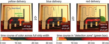
Mixing has been extensively studied in paper systems. Yager et al. devised an interesting method for sequential sample mixing and washing.Reference Lutz, Trinh, Ball, Fu and Yager 31 In this device, three “arms” of differing heights are simultaneously immersed in a fluid sample ( Figure 4 ). As the fluid is wicked from a reservoir, the level of fluid continuously drops until it breaks connection successively with each arm, thereby allowing for sequential reagent addition to occur across a given zone.Reference Lutz, Trinh, Ball, Fu and Yager 31 The system has the advantage of being completely autonomous and does not require valving etc. to manipulate fluid flow.
Autonomous sequential fluid delivery in a two-dimensional paper network (2DPN). Each leg wicked fluid from a single buffer source, and dried dyes representing reagents create different fluids from each leg (colors). Each colored fluid arrived at a different time at the “detection zone” (green box) and was shut off in a timed sequence after delivery. Some “bleeding” from the cellulose reagent pads can be seen as a narrow band that occupies about 20% of the strip width. Time courses show color across the full strip width or the detection zone as a function of time after device activation. For perspective, the 2DPN shown here is 2.5-fold larger in area than a conventional lateral flow test (LFT) (e.g., LFT: 5 mm × 40 mm = 200 mm2; 2DPN paper area: 500 mm2), but smaller devices (2DPN and fluid reservoir) can be made if desired. Reprinted with permission from Reference 31. © 2011 Royal Society of Chemistry.

Yager et al. also studied mixing in simple intersecting channel devices.Reference Osborn, Lutz, Fu, Kauffman, Stevens and Yager 10 The effects of channel dimensions and position were explored. Interestingly, laminar flow behavior, commonly observed in open-channel microfluidic devices, was still observed in these much wider paper-based channels.Reference Osborn, Lutz, Fu, Kauffman, Stevens and Yager 10 Whitesides et al. also studied mixing behavior in patterned paper microzone plates.Reference Carrilho, Martinez and Whitesides 32 Yeo et al. demonstrated rapid and consistent mixing in paper microfluidic devices using 30 MHz acoustic waves.Reference Rezk, Qi, Friend, Li and Yeo 11 Mixing efficiency was compared to simple diffusion within intersecting channels as well as intersecting channels in a tortuous path configuration.
Electronics on paper
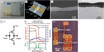
Further capability can be provided to paper by the addition of printed (or otherwise patterned) electronics ( Figure 5 ). This addition of electronics provides a direct route to quantitative diagnostic devices and other integrated systems. For example, wax-patterned devices on paper were developed to fit into a low-cost glucometer device for quantitative detection of several analytes.Reference Nie, Deiss, Liu, Akbulut and Whitesides 33 By simply changing the chemistry deposited onto the paper strips, assays beyond glucose could be performed with high precision.
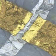
(a–b) Photographs of a 5-Euro currency with arrays of organic transistors and circuits and a magnified view of a single device. (c–d) Cross-section SEM and TEM of the self-assembled monolayer capacitor stack (Al/AlOx/SAM/Au)—a large part of what allows the devices to function on paper. (e) Performance of a CMOS inverter, a basic integrated circuit building block on paper demonstrating high gain and low leakage. Reprinted with permission from Reference 41. © 2011 Wiley.

Methods of performing immunoassays and nucleic acid detection using glucometers have also been developed.Reference Xiang and Lu 17 , Reference Xiang and Lu 19 An interesting adenosine sensor that combines printed electronic circuits with paper microfluidic channels was recently reported.Reference Liu, Xiang, Lu and Crooks 20 Various groups have explored methods for transforming paper into a conductive and energy storage material.Reference Nystroöm, Razaq, Strømme, Nyholm and Mihranyan 34 – Reference Hu, Choi, Yang, Jeong, La Mantia, Cui and Cui 36 Recently, Cui et al. deposited a carbon nanotube-based ink onto a paper substrate using simple coating methods.Reference Hu, Choi, Yang, Jeong, La Mantia, Cui and Cui 36 In addition to exhibiting resistance as low as 1 ohm/in2, the conductive paper showed dramatically improved adhesion to conductive inks when compared to plastics.
Additionally, Gleason et al. have shown significant progress in developing photovoltaic cells fabricated directly on paper, and while the efficiencies were low (~1%), the group has shown the cells to be very robust even after strenuous roll-to-roll processing.Reference Barr, Rowehl, Lunt, Xu, Wang, Boyce, Im, Bulović and Gleason 37 In both examples, the direct integration of energy storage and harvesting materials onto paper can provide a low-cost, robust source of power for integrated devices on paper.
There has also been considerable progress toward building more complex electronics on paper. Paper presents considerable challenges to conventional microelectronics processing techniques, namely high surface roughness and poor high temperature stability.Reference Tobjörk and Österbacka 16 Paper vendors are approaching these problems using unique surface coatings, and researchers have demonstrated a host of low temperature processed oxide and organic semiconductors.Reference Ito, Kon, Ishizaki and Sekine 38 , Reference Fortunato, Correia, Barquinha, Pereira, Gonçalves and Martins 39 Klauk et al. demonstrated high gain complementary organic circuits directly fabricated on currency notes using a self-assembled monolayer dielectric material, an impressive step toward fully integrated advanced security circuits on paper.Reference Eder, Klauk, Halik, Zschieschang, Schmid and Dehm 40 , Reference Zschieschang, Yamamoto, Takimiya, Kuwabara, Ikeda, Sekitani, Someya and Klauk 41 As an alternative approach to direct fabrication on paper, Rogers et al. have pioneered a versatile transfer method and flexible interconnect design, and demonstrated the transfer of fully fabricated circuits from silicon to other substrates.Reference Rogers, Someya and Huang 2 This method has the advantage that the underlying semiconductor materials (e.g., Si, GaAs) can be processed using conventional thin-film processing methods. The method has been shown to be capable of transferring flexible light-emitting diodes, sensors, and other logic directly onto paper, among other surfaces. The combination of flexible electronic devices with advances in paper fluidic devices provides exciting capabilities for diagnostic devices that are quantitative, inexpensive, and disposable.
Paper has even found application in the field of microelectromechanical systems (MEMs). Mazzeo et al. demonstrated fabrication of a paper accelerometerReference Liu, Mwangi, Li, O’Brien and Whitesides 42 as well as a paper touchpad keyboard.Reference Mazzeo, Kalb, Chan, Killian, Bloch, Mazzeo and Whitesides 43 While not as sensitive as traditional MEMs devices, the paper devices are considerably lower in cost and could prove useful in applications ranging from smart packaging to biomedical devices.
Beyond proof of concept
While still relatively new, integrated paper-based devices, of the sort described in this issue, are beginning to emerge from the prototype stage into products that solve specific needs in health care and other markets. One example is a liver function test that measures the levels of two liver enzymes, aspartate aminotransaminase (AST) and alanine aminotransaminase (ALT).Reference Pollock, Rolland, Kumar, Beattie, Jain, Noubary, Wong and Pohlmann 12 The device builds from an earlier prototypeReference Vella, Beattie, Cademartiri, Laromaine, Martinez, Phillips, Mirica and Whitesides 44 and is designed specifically for use with patients in the developing world taking anti-retroviral medications for treatment of HIV. Liver damage is a common side effect of these medications, and a low-cost, point-of-use, paper-based test provides a means for monitoring hepatotoxicity in regions with limited access to modern instrumentation. The paper-based test was recently shown to exhibit high accuracy in testing with clinical blood and serum specimens where the true results were unknown to the test operator.Reference Pollock, Rolland, Kumar, Beattie, Jain, Noubary, Wong and Pohlmann 12
In this issue
The articles in this issue provide a multidisciplinary view of how paper’s unique properties are being exploited to generate new fluidic and electronic devices. The article by Maxwell et al. demonstrates uniting patterned paper fluidic devices with printed electronics to generate novel low-cost quantitative diagnostic devices. Additionally, paper-based MEMs, keypads, and displays are described. The article by Lewis and Phillips describes a variety of functions that can be incorporated into multilayer paper microfluidic devices such as timers, chemical power supply, and an unconventional approach to quantitation, which requires neither electrodes nor the use of a handheld reader. Zheng et al. provide a detailed description of cellulose as a hierarchically structured material and discusses how this unique structure can be exploited to generate electrically conductive paper. Applications for transparent nanocellulose paper, a material with unique properties, are also presented. Fridley et al. provide a history of nitrocellulose and its use in diagnostics, describes the physics of fluid wicking in porous materials, and reviews advances in lateral flow technology. Sicard and Brennan describe the concept of “bioactive paper,” that is, paper that exhibits recognition properties. A detailed description of immobilization strategies for enzymes, antibodies, aptamers, and bacteriophage is provided along with a discussion on environmental sensing using paper devices.
Outlook
It is clear that novel uses for paper are still being discovered. In fact, despite the prevalence of paper, this field is arguably still in its infancy. As cost becomes an increasingly important factor in device production and distribution, low-cost recyclable materials, such as paper, are bound to play a key role. We have seen that researchers are developing innovative methods for manipulating fluid flow within fluidic devices based on wicking through paper. Such innovations provide a platform from which an entirely new class of diagnostic devices can be built. To be successful, these advances will draw from the fields of chemistry, electrical engineering, materials science, biotechnology, global health, medicine, and microfluidics. We have also seen how electronic devices, in a broad sense, can exploit the unique material properties of paper to generate low-cost, lightweight, and flexible components useful in energy storage, telecommunications, MEMs, packaging, and displays. The continued development of advanced and structured coatings on paper, novel electronic materials, and integration processes will be critical to the success of research in this domain. It is our hope that readers will be inspired by this issue to think differently about electronic and fluidic devices, particularly from a cost perspective. If devices are designed using low cost as a first principle, a tremendous global impact is possible—leading simultaneously to both larger market potential for the product and higher quality of life in developing nations.
Acknowledgments
The guest editors wish to thank the contributors of this issue. J.R. thanks the Bill and Melinda Gates Foundation, DARPA (contract number HR0011-12-2-0010), DFID, and USAID for their support of paper-based diagnostic devices.