Introduction
Recently, substrate-integrated waveguide (SIW) technology has attracted much attention due to its own advantages in high-Q, considerable power, low insertion loss, and easy fabrication [Reference Chen and Wu1]. Various types of SIW bandpass filters (BPFs) have been reported in past few years [Reference Deslandes and Wu2–Reference Chu, Hong, Dai, Tang, Chen, Hao, Zhu and Wu4]. Among these, dual-band and multi-band filters have a great theoretical and practical value in the modern radio frequency circuits. To support dual-band operation, examples of such efforts including cascading several SIW cavity resonators have been published [Reference Dong, Mo, He, Ma and Yang5]. However, the devices are too large. Then half-mode SIW filters are investigated for miniaturizing filter size, yet the device has disadvantage in high insertion loss [Reference Dong, Yang and Itoh6]. A miniaturized dual-band filter using dual-capacitively loaded SIW cavities is reported but it has a poor rejection in the outside of the passband [Reference Li, Chen and Chen7]. In [Reference Zhou, Kang and Wu8], a dual-band balanced BPF based on a double-layer SIW structure is proposed, but it is difficult to be applied to integrated circuits.
This letter introduces a novel single-cavity triangular SIW (TSIW) dual-band filter designed by etching a complementary triangular split ring resonator (CTSRR) on the top metal layer of TSIW cavity. Compared with conventional SIW, TSIW has particular advantages of easy integration and relatively small size [Reference Shen, Sun, Yin, Mao and Wei9]. The dual-band response is achieved by the resonant characteristic of the CTSRR and the degenerate modes of the TSIW.
The first-passband can be controlled by tuning the resonant frequency of the CTSRR, which mainly depends on its own size. In addition, the CTSRR etched on the surface of the TSIW produces a new transmission zero (TZ) in the upper stopband of the first-passband. Moreover, the feed points are shifted for effectively moving a TZ in the upper band to lower frequency in this design [Reference Chu10]. In order to adjust the TZs further, a pair of via-holes are introduced to generate perturbation. To verify the design, a single-cavity dual-band filter operating at 14.26 and 18 GHz is simulated, fabricated, and measured. The measured results are in line with the simulation results.
Filter design procedure
As a start point to design a multi-mode filter, the resonant characteristics of a TSIW cavity is calculated and simulated. The structure of the equilateral TSIW resonator is shown in Fig. 1. The resonant frequency of transverse magnetic (TM) modes in the equilateral TSIW resonator can be calculated by the following formula [Reference Wang11]:
 $$f\, = \,\displaystyle{{2c\sqrt {m^2\, + \,mn\, + \,n^2}} \over {3L\sqrt {\mu _r\varepsilon _r}}} $$
where μ r and ɛ r are relative permeability and permittivity of the substrate respectively, c denotes the velocity of light in vacuum, L is the length of the TSIW, m and n are integers and should satisfy m ≠ 0, n ≠ 0, and m + n ≠ 0.
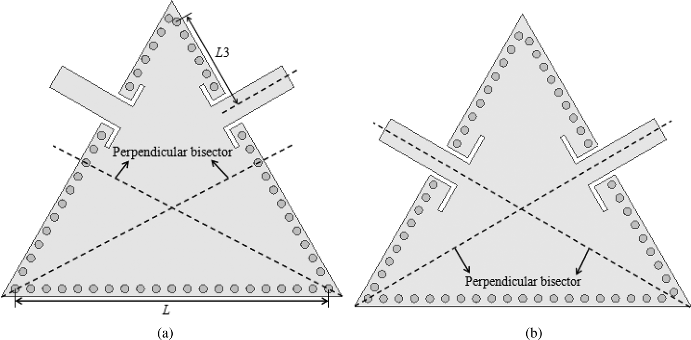
Configuration of the proposed equilateral TSIW.

Figure 1 describes two different structures designed on the basis of the same TSIW cavity.
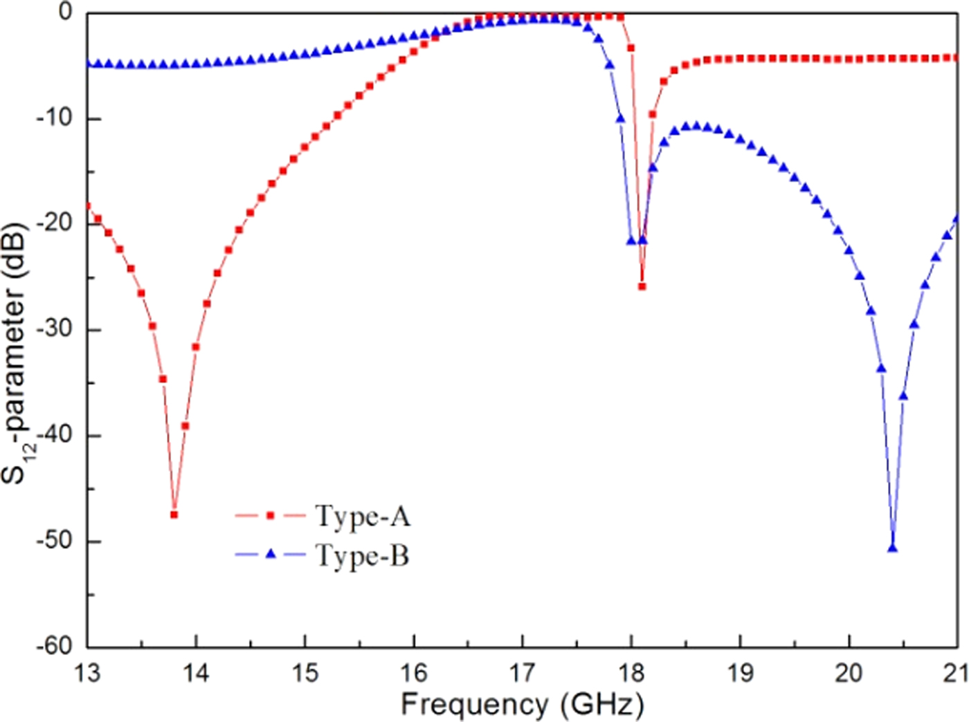
The feed points are shifted toward vertex as shown in Fig. 1(a). Comparison between the corresponding frequency responses obtained from two different structures is presented in Fig. 2.
Simulation responses of the proposed structures.
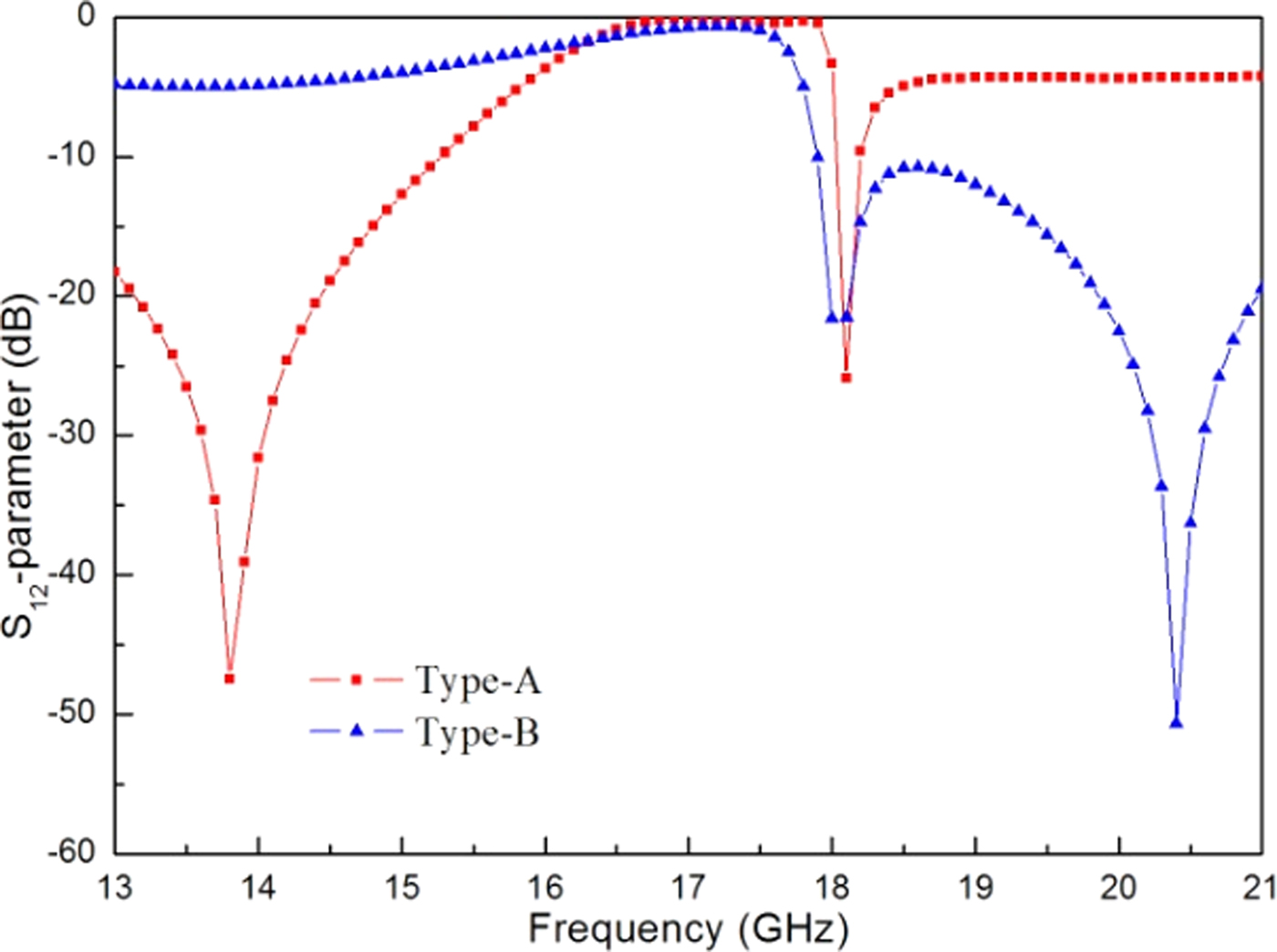
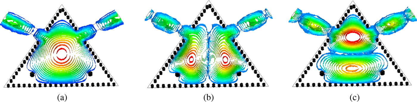
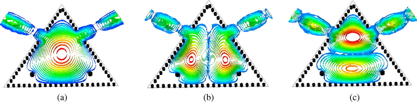
There are different responses that cover spectacular changes in the position of TZs. An available shift can relocate the feed point at the null of the electric resonance of the degenerate mode so as to control the TZs [Reference Chuang12]. Therefore, the shift can move a TZ in the upper band to lower frequency. However, the performance in upper band becomes poor after shifting the feeding lines. In order to improve the above limit and further adjust the TZs, a pair of metallic via-holes is utilized. The field distribution in the TSIW cavity with two metallic via-holes for three distinct modes is shown in Fig. 3. In this design, the degenerate modes are used to form the second passband.
Electric field distribution of type-A with two metallic via-holes for the fundamental mode and the two degenerate modes: (a) TM110, (b) TM210, and (c) TM120.
In order to form the first passband, a CTSRR etched on the top layer is introduced. The CTSRR is located at the perpendicular bisector of TSIW resonator, where the degenerate modes are hardly affected. In addition, the first passband can be controlled, because the resonant frequency of the CTSRR mainly depends on its own size. Meanwhile, a new TZ is produced in the upper first-passband.
Dual-band filter design
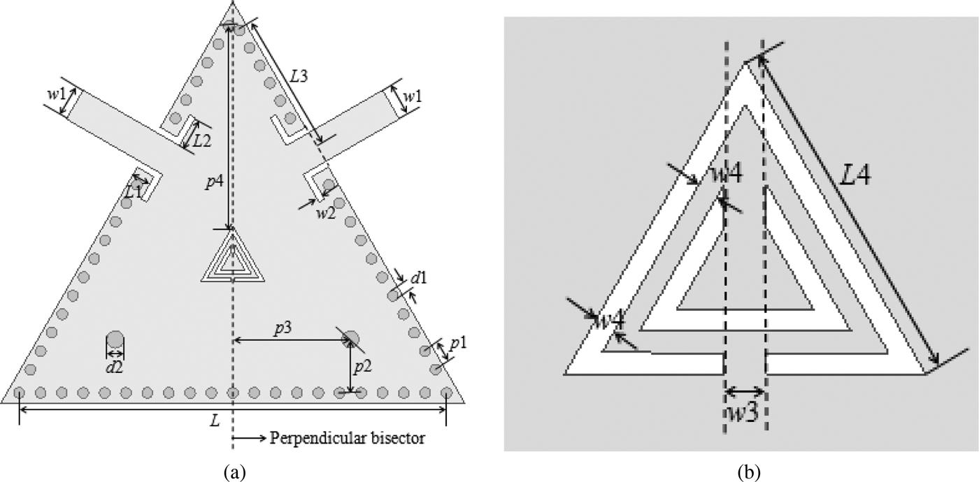
To demonstrate the design consideration, a single-cavity TSIW dual-band filter with a CTSRR is proposed as shown in Fig. 4. The dual-band filter is achieved by the CTSRR and the degenerate modes. The feed points are shifted toward vertex for moving a TZ in the upper band to lower frequency. The CTSRR etched on the top layer can produce a new TZ in the upper first-passband.
(a) Configuration of the proposed dual-band filter and (b) structure of the CTSRR.

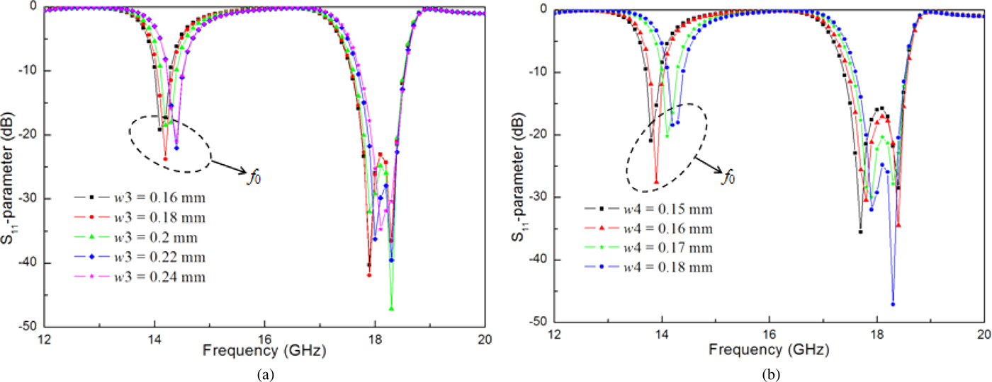
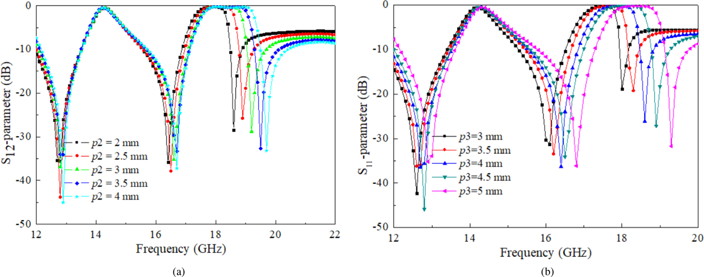
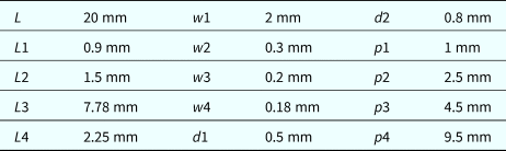
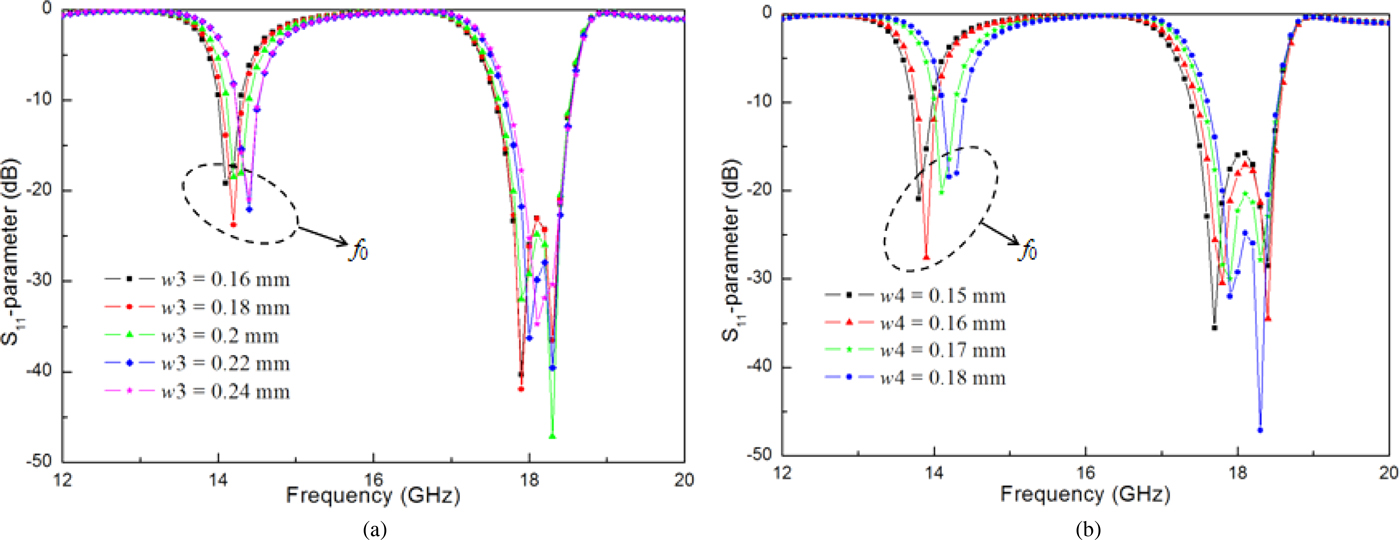
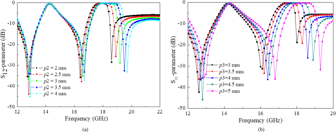
The center frequency of the first passband is controlled by the size parameters of the CTSRR. Figure 5 demonstrates the frequency responses of variable slit width (w3) and ring width (w4). The resonant frequency of the CTSRR is denoted by f 0. When w3 and w4 increase, f 0 gradually blueshifts. A pair of symmetric metallic via-holes about the perpendicular bisector is used to adjust the TZs. The functions of the variable position of the metallic via-holes (p2 and p3) are shown in Fig. 6. Table 1 shows the initial sizes of the dual-band filter.
Simulation responses of variable slit width (w3) and ring width (w4).
Simulation responses with variable position of the metallic via (p2 and p3).
Dimensions of the dual-band filter

Experimental results
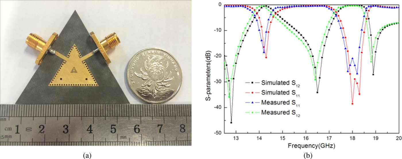
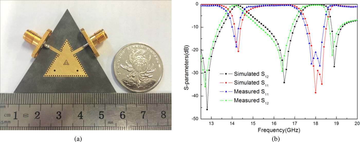
The single-cavity equilateral TSIW dual-band filter loaded on a CTSRR is fabricated and measured in this letter. Its photo is shown in Fig. 7(a). The substrate utilized in this device is the RT/duroid 5880 with ɛ r = 2.2 and thickness h = 1.508 mm. According to Fig. 7(b), the measured and simulated results have a good agreement. Two expected bands are operating at 14.26 and 18 GHz, respectively. The two 3-dB fractional bandwidths are 5 and 7%. Meanwhile, we can find that there are three TZs located at both sides of each passband. In addition, the passbands can both be controlled in this design.
(a) Photo of the dual-band filter and (b) simulated and measured results of the filter.
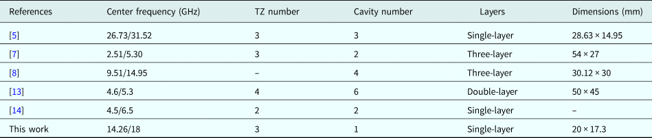
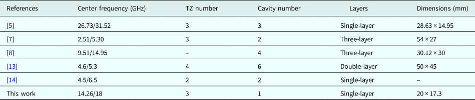
From the comparison between the proposed device and some previous dual-band filters listed in Table 2, our device has the advantages of individually controllable frequencies, simple structure, low cost, and high in-band performance.
Comparisons between dual-band filters
Conclusion
A single equilateral TSIW cavity loading an equilateral CTSRR is utilized to design a dual-band filter in this letter. The dual-band filter is achieved by the CTSRR and the degenerate modes of the TSIW cavity. Shifting the feeding points drives a TZ in the upper band to lower frequency. In order to improve the out-of-band performance, a pair of metallic via-holes is introduced. A CTSRR is utilized to achieve the first controllable passband and produce a new TZ. Finally, a single-cavity dual-band filter with three TZs at both sides of two passbands is simulated, fabricated, and measured. The experimental results are in line with the simulation results.
Acknowledgements
This work is supported by the National Natural Science Foundation of Jiangsu Province (BK20151512), and the Foundation of Nanjing University of Posts and Telecommunications (NY217085). Partial funding from the National Laboratory of Solid State Microstructures (M30050) is also much appreciated.
 Q. F. Geng was born in 1994. He graduated from the School of Physics and Electronic Science of Hubei Normal University with a bachelor's degree in 2017. In the same year, he continued to study his master's degree with the School of Information Materials and Nanotechnology of Nanjing University of Posts and Telecommunications. His research mainly includes millimeter waves, resonant rings, and spectrometers.
 H. J. Guo was born in 1990. She graduated from the School of Science of Nanjing University of Posts and Telecommunications with a bachelor of science degree in 2014. She graduated from the School of Materials of Nanjing University of Posts and Telecommunications with a master of engineering degree in optical engineering in June 2018. Her research mainly includes millimeter waves, resonant rings, and SIW filters.
 Y. Y. Zhu graduated from the Department of Physics of Nanjing University with a bachelor's degree in 1982 and received a doctor's degree in Condensed Matter Physics from the Department of Physics of Nanjing University in 1991. Since 1985, he has been working in the Physics Department of Nanjing University. He is currently a professor and doctoral supervisor in the School of Physics, Nanjing University. His research interests include optical and electronic functional microstructural materials including dielectric superlattice, metamaterials, plasmonic crystals, etc.
 Dr. Wei Huang graduated from Peking University in January 1992 and taught there. In December 1993, he went to Singapore to pursue postdoctoral research. In June 2006, he served as the Vice President of Nanjing University of Posts and Telecommunications; in July 2012, he served as the President of Nanjing University of Technology; and in June 2017, he served as the standing committee member and executive Vice President of the party committee of Northwest Polytechnic University.
 S. S. Deng was born in 1992. He graduated from the Science College of Nanjing University of Posts and Telecommunications with a bachelor's degree in science in 2014. In the same year, he studied in the School of Electronics and Optical Engineering and the School of Microelectronics in Nanjing University of Posts and Telecommunications. His research interests include rf circuits, millimeter-band filter design, and electromagnetic fields.
 Tao Yang received his B.Sci. and M.Eng. from the Department of Physics of Nanjing Normal University in 2001 and 2004, respectively. During 2004–2006, he took up a lecturing position at the Nanjing University of Posts and Telecommunications (NUPT). Then he studied at the Chinese University of Hong Kong (CUHK) as a Ph.D. student in 2006. After completing his Ph.D. thesis, he rejoined NUPT in 2009. He is currently a professor at NUPT. His research interests include optical spectrometers, photonic biosensors based on the surface plasmon resonance effect, optical memory, terahertz wave research, and so on.