I. INTRODUCTION
As shrinking of the critical dimensions in integrated circuits becomes increasingly difficult, semiconductor industry resorts to other approaches to achieve the objective of building new devices that consume less power but have higher performance. To this end, three dimensional integrated circuit (3D IC) architecture that allows higher performance in a much smaller package has been receiving wide attentions. Reference Wu, Kumar and Pamarthy1–Reference Hsiao, Liu, Lin, Liu, Lu, Huang, Chen and Tu3 In 3D IC packaging, interfaces between under bump metallizations (UBMs) and solder bumps play an important role in achieving a reliable interconnection. Reference Chen, Yu, Cheng, Tsai and Lu4,Reference Hsu, Huang, Huang, Chang and Wu5 Generally, the solder bumps need to go through several reflows during which solder/UBM liquid–solid interfacial reactions occur. Reference Wu, Kumar and Pamarthy1 There may be a temperature gradient existing during the reflow process in an oven or on a hot plate due to the differences in thermal conduction and dissipation among the chips, solder bumps, and substrate. For hot compression method, heat is applied through one of the chips and a temperature gradient across the micro bumps will be generated. Reference Zhan, Chuang, Juang, Lu, Chang and Trewehella6–Reference Chen, Hsiao, Chang, Ouyang and Tu8 In addition, due to the combined effect of current crowding and joule heating, solder alloy may melt locally Reference Huang, Tsai, Lin and Kao9,Reference Lin, Hu, Tsai, Kao and Tu10 and huge temperature gradient exceeding 2000 °C/cm may develop across the solder bumps in service. Reference Chen, Tong and Tu11 As the diameter of solder bumps is downsizing, issues caused by temperature gradient will become more serious.
Thermomigration (TM) is one of the simultaneous heat and mass transfer phenomena that occurs in a mixture, as a result of an external temperature gradient imposed across the mixture. Under a certain temperature gradient, TM occurs in solder joints. Reference Chen, Hsiao, Chang, Ouyang and Tu8,Reference Chen, Tong and Tu11–Reference Zhao, Zhong, Huang, Ma and Dong15 Since the interdiffusion of atoms between solder and UBMs can markedly affect the formation of interfacial intermetallic compounds (IMCs), liquid–solid TM which enhances the directional diffusion of metal atoms and induces the redistribution of elements will inevitably influence the growth behavior of interfacial IMCs during reflow. It is reported that the temperature gradient induced TM of Cu atoms can cause the asymmetrical growth and morphology of interfacial Cu–Sn IMCs between the cold and hot ends in Cu/solder/Cu solder joints. Reference Guo, Lin, Chen and Tu13–Reference Zhao, Zhong, Huang, Ma and Dong15 Under simulated temperature gradients of 136.50 °C/cm at 250 °C and 154.50 °C/cm at 280 °C in Cu/Sn/Cu solder joints, the growth of the Cu6Sn5 IMC layers at the cold end was fast and it followed the linear law with reflow time while that at the hot end was strongly inhibited. Reference Zhao, Zhong, Huang, Ma and Dong15
The Cu/solder/Ni material system is commonly used as a typical interconnecting structure in electronic packaging technologies. The interfacial reactions between Ni and Sn-based solders have been reported to be quite sensitive to the Cu concentration in the solders, Reference Ho, Tsai, Lin and Kao16 and Ni also has a strong effect on the interfacial reactions of solder/Cu during reflow. Reference Liu, Ho, Peng and Kao17 A continuous (Ni1−x ,Cu x )3Sn4 layer formed at solder/Ni interface when the Cu concentration in the solder was less than or equal to 0.3 wt% and a continuous (Cu1−x ,Ni x )6Sn5 layer formed at the interface if the Cu concentration was higher than 0.6 wt%. Reference Ho, Tsai, Lin and Kao16–Reference Ho, Yang and Kao19 It was also reported that the Cu and Ni atoms could diffuse to the opposite side to form interfacial (Cu x ,Ni1−x )6Sn5 or (Ni y ,Cu1−y )3Sn4 IMCs in Cu/solder/Ni solder joints during reflow, showing strong Cu–Ni cross-interactions. Reference Ho, Yang and Kao19 With the occurrence of Cu–Ni cross-interaction, the growth rate of the IMC layer at the Sn/Ni interface was relatively larger than that at the Sn/Cu interface after a long term reflow. Moreover, the consumption of the Cu substrate could be greatly enhanced by the presence of Ni. Reference Ho, Yang and Kao19–Reference Huang, Hsiao, Chen and Tu22 However, no attention seems to be paid to the Cu–Ni cross-interaction under temperature gradient though it might induce a serious reliability issue.
In the previous studies, synchrotron radiation real-time imaging technology has been proven to be an effective method to in situ observe the growth behavior of interfacial IMCs and bubbles in solder joints during reflow and liquid–solid electromigration. Reference Mohd Salleh, McDonald, Yasuda, Sugiyama and Nogita23–Reference Huang, Zhang, Zhao and Zhou25 In the present study, synchrotron radiation real-time imaging technology was used to in situ study the interfacial reactions in Cu/Sn/Ni solder joints under temperature gradient during reflow on a hot plate. The Cu–Ni cross-interaction and its effects on interfacial IMC growth and substrate consumption were discussed.
II. EXPERIMENTAL
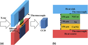
The Cu/Sn/Ni solder joints were prepared by immersion soldering at 250 ± 2 °C for 30 s. A Cu plate (99.95%) and a Ni plate (99.99%) were prepared with one surface being carefully ground, polished, and cleaned in ethanol. After the polished faces were aligned and fixed, the whole configuration was immersed into a pure Sn (99.99%) bath. The gap between the Cu and Ni plates was controlled by two stainless spacers. After immersion soldering, the specimen was cooled immediately in water to room temperature and cut into thin solder joints followed by grinding and polishing. The final cross-section of the Cu/Sn/Ni solder joints was 100 μm × 300 μm in dimension and the Sn solder layer between the Cu and Ni substrates was about 90 μm in thickness. Figure 1 shows the schematic of the experimental figuration. Silicone grease with a high thermal conductivity was used to fix the solder joint onto the heat source and heat sink. Two experimental conditions of A and B with Ni substrate close to the heat source and the heat sink, respectively, were conducted in this study. Table I shows the temperatures of the solder joints measured by an Omega K-type thermocouple during the heat preservation stage.
Schematic diagrams of (a) the experimental configuration of the synchrotron radiation real-time observation and (b) the tested solder joints.

Temperatures measured in the Cu/Sn/Ni solder joints under different experimental conditions.

Synchrotron radiation real-time imaging experiments were carried out at the Beam line BL13W1 of the Shanghai Synchrotron Radiation Facility (SSRF). A charged couple device camera with a resolution ratio of 0.325 μm/pixel and an exposure time of 3 s/frame was used to catch and collect the images. To facilitate the microstructure observation and phase analysis, another two Cu/Sn/Ni solder joints experienced the same soldering process as that in the synchrotron radiation experiments were cooled down in water immediately after reflow. Then the microstructure of the solder joints was examined using a scanning electron microscope (SEM) equipped with an energy dispersive x-ray (EDX) spectrometer. The average thicknesses of the interfacial IMCs and the consumption of the substrates at both the hot and cold ends were analyzed by image-process software. The temperature distribution across the solder layer undergoing TM was simulated by finite element method (FEM). Table II lists the thermal conductivities of the constituent components of the samples.
Thermal conductivities of the constituent components of the samples used for simulation.

III. RESULTS AND DISCUSSION
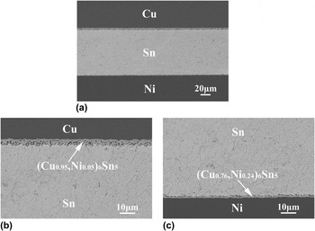
Figure 2 shows the cross-sectional microstructure of an as-soldered Cu/Sn/Ni solder joint. A continuous (Cu0.95,Ni0.05)6Sn5 IMC layer of 2.64 μm in thickness formed at the Cu/Sn interface, while a continuous (Cu0.76,Ni0.24)6Sn5 IMC layer of 1.16 μm in thickness formed at the Ni/Sn interface. That is, Cu–Ni cross-interaction occurred at both interfaces in the as-soldered state. However, the (Cu,Ni)6Sn5 IMC at the Cu/Sn interface showed a faster growth rate than that at the Ni/Sn interface during a short time reflow.
Microstructure of an as-soldered Cu/Sn/Ni solder joint: (a) macrograph, (b) Cu/Sn interface, and (c) Ni/Sn interface.

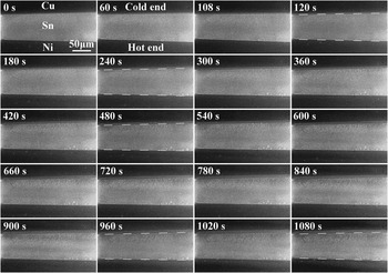
Figure 3 shows the synchrotron radiation images of the Cu/Sn/Ni solder joint with the Ni substrate as the hot end during the reflow process, i.e., condition A. 0 s was the moment at which the solder started to melt, 0–60 s was the heating stage after which the temperature of the bottom Ni substrate reached 290 °C, and 60–1080 s was the heat preservation stage. The white dashed lines in the images indicate the initial positions of the Cu/Sn and Ni/Sn interfaces. After reflowing for 60 s, a thin, laminar-like IMC layer formed at each liquid–solid interface. After reflowing for 300 s, the interfacial IMC layer at the cold end grew much thicker while that at the hot end remained thin, indicating the occurrence of asymmetrical IMC growth between the cold and hot ends. Thereafter, this asymmetrical growth became more and more obvious, since the interfacial IMC at the cold end grew continuously while that at the hot end remained stable. After reflowing for 420 s, many rod-like IMC grains formed on the top of the laminar-like IMC at the cold end and grew into the molten solder. After reflowing for 1080 s, a bilayer structure was clearly observed at the cold end, with the thick, laminar-like IMC layer close to the Cu substrate and the rod-like IMC grains penetrated into the molten solder. In addition, the consumption of the Cu cold end was significant, which was distinctly different from the previous observations in Cu/Sn/Cu solder joints. Reference Zhao, Zhong, Huang, Ma and Dong15 However, the consumption of the Ni hot end was quite limited even after reflowing for 1080 s.
Synchrotron radiation images of the Cu/Sn/Ni solder joint with the Ni substrate as the hot end during reflow (condition A). 0 s: solder melted, 0–60 s: heating stage, and 60–1080 s: heat preservation stage.

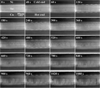
Figure 4 shows the synchrotron radiation images of the Cu/Sn/Ni solder joint with the Cu substrate as the hot end during the reflow process, i.e., condition B. 0–48 s was the heating stage after which the temperature of the bottom Cu substrate reached 283 °C and 48–1080 s was the heat preservation stage. The white dashed lines in the images indicate the initial positions of the Cu/Sn and Ni/Sn interfaces. After reflowing for 48 s, a ruderal IMC layer formed at the cold end while a thin, laminar-like IMC layer formed at the hot end. After reflowing for 120 s, the ruderal IMC layer at the cold end grew much thicker with many rod-like IMCs penetrating into the molten solder while the laminar-like IMC layer at the hot end remained thin, indicating that the asymmetrical IMC growth between the two ends occurred. Meanwhile, the spalling of the laminar-like IMC layer from the Cu hot end was clearly observed, which may result from the fast dissolution of the Cu substrate. Thereafter, the interfacial IMC at the cold end continuously grew toward the hot end, while the spalled IMC layer at the hot end gradually dissolved and finally disappeared at 600 s. After reflowing for 1080 s, many of the rod-like IMCs reached the opposite hot end. Moreover, no obvious consumption of the Ni cold end was observed whereas the Cu hot end was seriously consumed.
Synchrotron radiation images of the Cu/Sn/Ni solder joint with the Cu substrate as the hot end during reflow (condition B). 0 s: solder melted, 0–48 s: heating stage, and 48–1080 s: heat preservation stage.

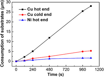
Combining the observations in Figs. 3 and 4, the interfacial IMCs at the Ni cold end were obviously thicker than those at the Cu cold end, while those at both the Cu and Ni hot ends were relatively thin. The consumption of the Ni substrates was quite limited regardless of the cold or hot end. However, the consumption of the Cu substrates was always obvious, especially as the hot end. Figure 5 shows the consumption of the Ni and Cu substrates as a function of reflow time. The data of the Ni cold end were not involved in Fig. 5 due to the no obvious consumption. After reflowing for 1080 s, the consumption of the Ni hot end, Cu cold end, and Cu hot end was 1.68 μm, 5.34 μm, and 28.06 μm, respectively.
Consumption of the Ni and Cu substrates as a function of reflow time.

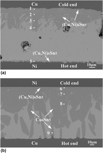
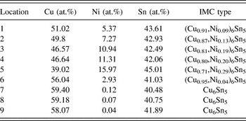
Another two Cu/Sn/Ni solder joints that experienced the same reflow processes in the synchrotron radiation experiments were cooled down in water immediately. Figure 6 shows the SEM images of the Cu/Sn/Ni solder joints after solidification. According to the EDX analysis, the compositions of the interfacial IMCs at different positions in Fig. 6 were listed in Table III. When Ni substrate was the hot end, (Cu,Ni)6Sn5-type IMCs formed at the two interfaces, indicating that Cu–Ni cross-interaction occurred at both the hot and cold ends. At the Cu cold end, the scattered (Cu,Ni)6Sn5 IMC grains formed on the top of the laminar (Cu,Ni)6Sn5 IMC with a total thickness of 24.02 μm which was comparable to that at the anode Sn/Cu interface in Cu/Sn/Ni solder joint that undergone electromigration at 250 °C under 5.0 × 10³ A/cm2 for the same duration. Reference Huang, Zhang, Ma and Chen28 At the Ni hot end, the thin laminar (Cu,Ni)6Sn5 IMC was only 2.22 μm thick. When Cu substrate was the hot end, (Cu,Ni)6Sn5 IMC close to the Ni substrate and Cu6Sn5 IMC close to the solder with a total thickness of 75.58 μm formed at the Ni cold end, which was about three times thicker than those formed at the Cu cold end. However, an extremely thin Cu6Sn5 layer and several large Cu6Sn5 grains were observed at the Cu hot end. That is, the Cu–Ni cross-interaction only occurred at the cold end. In addition, no obvious consumption of the Ni cold end was identified by the smooth Ni/(Cu,Ni)6Sn5 interface. Obviously, the phenomena observed in the present study were quite different to the observations in the Cu/Sn/Ni solder joints during isothermal reflow by Wang and Liu. Reference Wang and Liu18 TM significantly influenced the Cu–Ni cross-interaction as well as the interfacial reactions in the Cu/Sn/Ni solder joints during reflow.
SEM images of the Cu/Sn/Ni solder joints after experiencing the same soldering process: (a) Ni substrate as the hot end (condition A), and (b) Cu substrate as the hot end (condition B).

Compositions of the interfacial IMCs at different positions in Fig. 6.

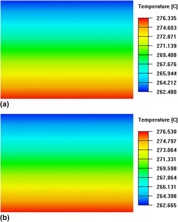
The temperature distribution in the liquid solder layer during reflow on the hot plate was simulated by FEM. Figure 7 shows the simulation results. For the condition A, as shown in Fig. 7(a), the highest temperature of the solder layer was 276.335 °C at the bottom Ni/Sn interface and the lowest temperature was 262.480 °C at the top Cu/Sn interface, generating a temperature difference (ΔT) of 13.855 °C across the solder layer. The resulting temperature gradient between the cold and hot ends was 1539.44 °C/cm, which was smaller than that in solid state TM by Ouyang et al. Reference Ouyang, Jhu and Chang12 ΔT/T m (=0.06) was small, where T m is the melting point of pure Sn, the average temperature of 269.41 °C was assumed as the working temperature. Similarly for the condition B, shown in Fig. 6(b), the resulting temperature gradient between the cold and hot ends was 1540.56 °C/cm and the working temperature was assumed as 269.59 °C. Since no external field, such as electric or stress, was introduced during the reflow process, temperature gradient across the solder was responsible for the abnormal IMC growth and substrate dissolution.
Simulated temperature distribution in the liquid solder layer during reflow on hot plate: (a) Ni substrate as the hot end (condition A), and (b) Cu substrate as the hot end (condition B).

The atomic diffusion flux undergoing TM can be given as follows Reference Chen, Hsiao, Chang, Ouyang and Tu8
 $$J = {J_{{\rm{chem}}}}{\rm{ + }}{J_{{\rm{TM}}}}{\rm{ = }} - D\left( {{{\partial C} \over {\partial x}}} \right) + C{D \over {{\rm{k}}T}}{{Q^*} \over T}\left( { - {{\partial T} \over {\partial x}}} \right)\quad ,$$
where J
chem is the flux caused by chemical potential gradient, J
TM is the flux caused by temperature gradient, D is the diffusivity, C is the concentration, k is the Boltzman constant, T is the temperature, Q* is the heat of transport,
 $\partial C/\partial x$
is the concentration gradient, and
 $\partial T/\partial x$
is the temperature gradient.
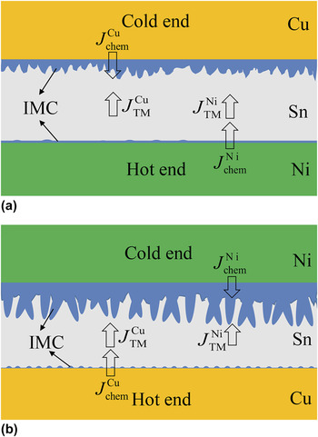
Figure 8 shows the schematic diagrams of the atomic fluxes in the Cu/Sn/Ni solder joints undergoing TM. For the condition A, as shown in Fig. 8(a), the Ni and Cu atomic fluxes,
 $J_{{\rm{Sn}}}^{{\rm{Cu}}}$
and
 $J_{{\rm{Sn}}}^{{\rm{Ni}}}$
, in the liquid Sn can be written as follows
 $$J_{{\rm{Sn}}}^{{\rm{Cu}}} = J_{{\rm{chem}}}^{{\rm{Cu}}} - J_{_{{\rm{TM}}}}^{{\rm{Cu}}}\quad ,$$
 $$J_{{\rm{Sn}}}^{{\rm{Ni}}} = J_{{\rm{chem}}}^{{\rm{Ni}}} + J_{_{{\rm{TM}}}}^{{\rm{Ni}}}\quad ,$$
where
 $J_{{\rm{chem}}}^{{\rm{Cu}}}$
and
 $J_{{\rm{TM}}}^{{\rm{Cu}}}$
are the Cu atomic fluxes and
 $J_{{\rm{chem}}}^{{\rm{Ni}}}$
and
 $J_{_{{\rm{TM}}}}^{{\rm{Ni}}}$
are the Ni atomic fluxes induced by the chemical potential gradient and TM, respectively.
Schematic diagrams of atomic fluxes in the Cu/Sn/Ni solder joints undergoing TM: (a) Ni substrate as the hot end (condition A), and (b) Cu substrate as the hot end (condition B).

Since
 $J_{{\rm{chem}}}^{{\rm{Cu}}}$
and
 $J_{{\rm{TM}}}^{{\rm{Cu}}}$
are in the opposite directions, the diffusion of the Cu atoms from the cold end to the hot end is significantly retarded. However,
 $J_{_{{\rm{TM}}}}^{{\rm{Ni}}}$
and
 $J_{{\rm{chem}}}^{{\rm{Ni}}}$
are in the same direction, resulting in an enhanced and steady diffusion of the Ni atoms from the hot end to the cold end. At the Cu cold end, the enhanced diffusion of the Ni atoms to the interface can greatly reduce the Cu solubility in the molten Sn, which enlarges
 $J_{{\rm{chem}}}^{{\rm{Cu}}}$
. As a result, the consumption of the Cu substrate becomes much more serious in this study comparing with that in Cu/Sn/Ni solder joint during isothermal reflow by Wang and Liu
Reference Wang and Liu18
and that at the cold end in Cu/Sn/Cu solder joint during TM by Zhao et al.
Reference Zhao, Zhong, Huang, Ma and Dong15
Since it is difficult to diffuse against temperature gradient, most of the dissolved Cu atoms take part in the interfacial reaction along with the Ni atoms from the hot end, resulting in the fast IMC growth. Thus, the combined effect of Cu–Ni cross-interaction and TM accelerates the Cu dissolution and the IMC growth at the Cu cold end. Moreover, the change of the IMC morphology from laminar-like to rod-like is most probably associated with the increasing Ni content in the (Cu,Ni)6Sn5 IMCs, as shown in Table III. Many researchers have reported that high Ni-containing (Cu,Ni)6Sn5 compounds tend to have a needle-like shape.
Reference Ho, Tsai, Lin and Kao16–Reference Wang and Liu18
At the Ni hot end, a small amount of the dissolved Cu atoms can diffuse antitemperature gradient to the hot end, which enables the IMCs at the Ni/Sn interface remaining as (Cu,Ni)6Sn5. Although the Ni atoms can continuously diffuse through the (Cu,Ni)6Sn5 layer to the interface with the molten Sn, they are easily forced to diffuse to the opposite cold end by the combination of the chemical potential gradient and temperature gradient, leaving few Ni atoms to take part in the interfacial reaction. As a result, the (Cu,Ni)6Sn5 IMCs at the hot end remain thin. Moreover, comparing the morphologies of the (Cu,Ni)6Sn5 IMCs at the two interfaces in Fig. 6(a), we believe that the Ni atoms can easily reach the top of the opposite Sn/(Cu,Ni)6Sn5 interface under temperature gradient. The significantly larger growth rate of the IMC layer at the Cu/Sn interface over that at the Ni/Sn interface is attributed to both the continuous TM of the Ni atoms from the hot end and the fast dissolution of the Cu cold end.
For the condition B, as shown in Fig. 8(b), the Cu and Ni atomic fluxes in the liquid Sn can be written as follows
 $$J_{{\rm{Sn}}}^{{\rm{Cu}}} = J_{{\rm{chem}}}^{{\rm{Cu}}} + J_{_{{\rm{TM}}}}^{{\rm{Cu}}}\quad ,$$
 $$J_{{\rm{Sn}}}^{{\rm{Ni}}} = J_{{\rm{chem}}}^{{\rm{Ni}}} - J_{_{{\rm{TM}}}}^{{\rm{Ni}}}\quad .$$
Since
 $J_{{\rm{chem}}}^{{\rm{Cu}}}$
and
 $J_{{\rm{TM}}}^{{\rm{Cu}}}$
are in the same direction, the diffusion of the Cu atoms from the Cu hot end to the Ni cold end is significantly enhanced. Whereas,
 $J_{_{{\rm{TM}}}}^{{\rm{Ni}}}$
and
 $J_{{\rm{chem}}}^{{\rm{Ni}}}$
are in the opposite directions, resulting in a negligible Ni atomic flux. At the Cu hot end, as Ni atoms can hardly diffuse through the thickening IMC and migrate to the hot end against temperature gradient, the IMC at the Cu/Sn interface transforms from the initial (Cu,Ni)6Sn5 into the present Cu6Sn5. Under the combination of chemical potential gradient and temperature gradient, Cu atoms are impelled to migrate toward the cold end by an enhanced driven force. Consequently, the consumption of the Cu substrate is accelerated. With the continuous dissolution of the Cu substrate, the laminar-like (Cu,Ni)6Sn5 IMC finally spall from the interface. As most of the dissolved Cu atoms diffuse away, the newly formed Cu6Sn5 layer remains extremely thin. At the Ni cold end, massive Cu atoms migrate to the Ni/Sn interface, which facilitates the fast IMC growth. Since few Ni atoms can diffuse across the thickening IMC layer antitemperature gradient, large Cu6Sn5 grains form on the top of the (Cu,Ni)6Sn5 layer. The Ni substrate is scarcely dissolved. The Cu–Ni cross-interaction is suppressed at the cold Ni/Sn interface and eliminated at the hot Cu/Sn interface. TM has strong effects on the Cu–Ni cross-interaction and the interfacial reactions in the Cu/Sn/Ni solder joints during reflow. TM should become an important consideration in 3D IC packaging technologies.
IV. CONCLUSION
The asymmetrical IMC growth and substrate consumption in the Cu/Sn/Ni solder joints undergoing TM were in situ observed distinctly, i.e., the interfacial IMCs at the cold end grew remarkably faster than that at the hot end, and the Cu consumption was serious while the Ni consumption was limited, whether it was at the hot or cold end. The temperature gradient significantly influenced the Cu–Ni cross-interaction. With Ni as the hot end, the Ni atomic flux toward the cold end was enhanced, whereas the Cu atomic flux toward the hot end was restrained. The Cu–Ni cross-interaction occurred at both interfaces, resulting in the interfacial IMCs maintaining (Cu,Ni)6Sn5. Under the combined effect of Cu–Ni cross-interaction and TM, the rapid interfacial IMC growth and the abnormally fast Cu consumption occurred the cold end. With Cu as the hot end, the Cu atomic flux toward the cold end was obviously enhanced, whereas the Ni atomic flux toward the hot end was eliminated. The Cu–Ni cross-interaction only occurred at the Ni/Sn interface, resulting in the transformation of (Cu,Ni)6Sn5 into Cu6Sn5 and the serious consumption of the Cu at the Cu/Sn interface. Cu imposed more damaging effect than Ni under temperature gradient.
ACKNOWLEDGMENTS
This work was supported by the National Natural Science Foundation of China (Grant Nos. 51301030 and 51571049), the Specialized Research Fund for the Doctoral Program of Higher Education of China (Grant No. 20120041120038) and the Fundamental Research Funds for the Central Universities (Grant No. DUT15ZD239). The synchrotron radiation experiments were performed at the BL13W1 beam line of Shanghai Synchrotron Radiation Facility (SSRF).