I. INTRODUCTION
Electronic skins, which are used in wearable electronics, prosthetic limbs, robotic skins, and more other application areas, possess a high degree of flexibility and stretchability, and can sense pressure, shear, strain, temperature, humidity, fluid flow, and so on. Reference Wagner, Lacour, Jones, Hsu, Sturm, Li and Suo1–Reference Wang, Huang, Ma, Liu, Liu and Zhang6 A lot of research focuses on the electronic skin systems based on resistive, capacitive, and piezoelectric. Reference Zhou and Wang7–Reference Li and Wen9 Recently, flexible composites with piezoresistive properties have been proved to be a good choice since these materials are able to reproduce the tactile sense and fit the shape of the robot structure, obtaining the high conformability required to mimic the human skin and being able to obtain metrical information with high precision and high resolution. Reference Stassi, Cauda, Canavese and Pirri10,Reference Yang, Cheng, Chang, Tsao, Yang, Shih, Chang, Changa and Fan11 Composites containing dispersed conductive fillers in an insulating matrix have been studied for flexible force sensor applications. Reference Canavese, Stassi, Stralla, Bignardi and Pirri12,Reference Yu and Kwon13 Particularly, conductive polymer composites containing carbon-based fillers have received considerable attention because of their high conductivity, low density, ease of processing, and so on. Reference Yoshimuraa, Nakanoa, Okamotoa and Miyakeb14–Reference Tamburrano, Sarasini, De Bellis, D’Aloia and Sarto18 There are mainly four types of carbon fillers used: carbon black (CB), graphite (G), carbon fiber (CF), and carbon nanotubes (CNTs). Reference Cravanzola, Haznedar, Scarano, Zecchina and Cesano19,Reference Arboleda, Ares, Abad, Ferreira, Costa and Lanceros-Mendez20 Some polymer-based composites containing two different carbon fillers (e.g., CF and CB, CNTs and G) have also been investigated, which led to synergistic effects on network formation in the inner of the composite and improved the piezoresistive properties. Reference Kumar, Sun, Caceres, Li, Wood, Perugini, Maguire and Zhong21,Reference Sun, Bao, Guo and Yu22
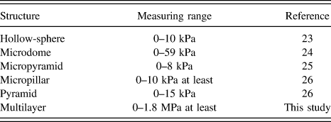
Although the flexible composites have shown many advantages, low sensitivity, slow response, and signal drifts with temperature are preventing them from applications. To overcome these shortcomings, structural optimizations on the flexible composites were researched. Pan presented a pressure sensor based on hollow-sphere microstructure-induced elasticity in conducting polymer film which can detect pressures of less than 1 Pa and exhibited a short response time, good reproducibility, and excellent cycling stability. Reference Pan, Chortos, Yu, Wang, Isaacson, Allen and Bao23 Park introduced and demonstrated a design of flexible electronic skins based on composite elastomer films that contained interlocked microdome arrays and displayed giant tunneling piezoresistance, which showed an extreme resistance-switching behavior (R OFF/R ON of 105). Reference Park, Lee, Hong, Ha, Jung, Lim and Ko24 In addition to these, micropyramid, micropillar, and other structure resistive pressure sensors were presented and researched. Reference Choong, Shim, Lee, Jeon, Ko, Kang and Chung25,Reference Park, Lee, Lim, Lee, Jung, Lim and Ko26 These sensors with different structural optimizations obtained high sensitivity and other excellent properties; however, the unstable contact resistance in the low-pressure regime and small workable pressure range (Table I) were the common drawbacks of them. When encountering a large impact loading, these pressure sensors will be unable to obtain the pressure information and prompt actuators (robots, humans, or others) to respond to the loading timely. To overcome these shortcomings, a multilayered flexible piezoresistive sensor based on CNTs/CB/SR conductive composite was designed and investigated in this study, which has a large workable pressure range.
Comparison of pressure measuring range between multilayered piezoresistive sensor and sensors with other structures.

II. EXPERIMENTS
A. Materials
Silicone rubber (SR-GD401; dielectric constant: 3.0) was provided by Sichuan Zigong CHENGUANG Chemical Institute. The carbon black (CB-3100) exhibits an average particle size of about 30 nm (according to the manufacturer), and was provided by Swiss SPC Chemical Company. The multiwalled CNTs (MWCNTs-TNM5) exhibit an average diameter of about 20–30 nm with length of about 10–30 μm (according to the manufacturer), and were purchased from Chengdu Organic Chemicals Co., Ltd. The hexane (purity ≥95 wt%) was provided by Dongguan United Chemical Co., Ltd. The copper wire meshes (mesh number: 40 and thickness: 0.2 mm) were purchased from Guangzhou MINWAN Mesh Co., Ltd. The indium tin oxide (ITO)-coated (thickness: 180 nm) conductive flexible polyethylene terephthalate (PET) sheet (thickness: 150 μm) was acquired from Zhuhai Kaivo Optoelectronic Technology Co., Ltd.
B. Structure design of sensor element
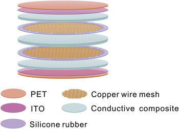
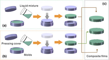
As shown in Fig. 1, the multilayered piezoresistive sensor includes three conductive composite (CNTs/CB/SR) films, two copper wire meshes and two ITO/PET sheets. (To show more clearly, the ITO/PET films are shown separately. Actually, the ITO and PET films are not separate but a single piece.) The three flexible conductive composite films, as the piezoresistive sensitive part, are not a simple planar structure, as shown in Fig. 2, the top and bottom layers have the same structure: one side is planar and the other side is wave-like, while the surfaces of the middle layer are both wave-like. (Radius of each semicylindrical wave is 0.6 mm.) Moreover, the waves of the adjacent layers are perpendicular to each other. The preparation process of this conductive composite will be described in detail in the next section. Then the two copper wire meshes were inserted between the adjacent layers, respectively. The edges of copper wire meshes were coated with SR, which acted as glue to make the films be adhered with each other. Two ITO/PET sheets, which acted as electrodes, were covered onto the surface of composite films during the vulcanization of the composite so that the electrodes can be firmly adhered with the composite. Reference Wang and Li27 Furthermore, the PET sheets also played the role of encapsulation films to the whole sensor element. The wires were connected with the ITO electrodes by conductive silver adhesive. The dimension of the sensor element is round with diameter of 25 mm and thickness of 5 mm. To have a better comparison, sensor elements with another two different configurations were designed: a multilayered structure without copper wire meshes; a single monolayered structure (the thickness of them was also 5 mm). Compared with the multilayered structure that we chose finally, the multilayered structure without copper wire meshes also has three conductive composite films as described above but no copper wire meshes, and the single monolayered structure has no copper wire meshes and only one conductive composite film with planar surfaces.
Schematic of multilayered piezoresistive sensor.

Manufacturing process of the CNTs/CB/SR composite films.

C. Composite manufacturing
The conductive composite consists of CNTs and CB as conductive fillers and SR as insulating matrix. The mass ratio of conductive fillers to SR is 0.08 (volume fraction: 0.22, near the percolation threshold, the sensitive material will have obvious piezoresistive phenomenon) and the ratio of CNTs and CB was set to 2:3, which had low resistivity, good dispersion, superior and stable piezoresistive performance according to our previous studies. Reference Liu, Gao, Cai, Liu, Miu and Huang28 The conductive composite was produced using a magnetic stirrer. First, hexane was added into CNTs and CB powder followed by mechanical stirring for 30 min and sonication for 20 min to obtain a well-dispersed filler suspension. Second, the SR was added into the filler suspension. After 1 h of high-shear magnetic mixing with a rotational speed of 3000 rpm at room temperature, the mixture was kept in a vacuum oven at 80 °C for 5 h to remove the residual solvent. Finally, the mixture was poured into the special molds, which were manufactured by 3D printing technology. As shown in Fig. 2, the mixture was clamped between the mold and pressing cover with a little positive pressure during the cross-linking at room temperature for 2 days to complete the curing process to obtain better desired shaped films.
III. RESULTS AND DISCUSSION
A. Characterization
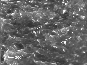
The microstructures of the conductive composite films were examined by a scanning electron microscope (SEM, Sirion200, FEI Company, Portland, OR). The acceleration voltage used during SEM characterization is 10 kV. Figure 3 shows the SEM micrograph of the fractured surface of the CNTs/CB/SR composite. It shows the filler dispersion and distribution at the percolation threshold in polymer composites. The CNTs and CB were uniformly distributed, which formed the conductive network Reference Alig, Lellinger, Engel, Skipa and Pötschke29–Reference Gao, Li, Meng and Yang31 in the SR matrix.
SEM image of the CNTs/CB/SR composite.

B. Piezoresistive properties and analysis
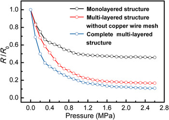
The pressure, which ranged from 0 to 2.6 MPa, was applied on the sensor element by the pressure testing machine (WDW-05), which was purchased from Changzhou SANFENG Instrument Technology Co., Ltd. And the electrical resistance of the samples was recorded by a LCR meter (GW INSTEK LCR-819, Good Will Instrument Company Ltd., Taiwan, China). Figure 4 shows the schematic of the test setups. To demonstrate and quantify the effects of the multilayered structure on piezoresistance, we compared the electrical resistances of sensor elements with three different configurations: a single monolayered structure, a multilayered structure without copper wire meshes, and the complete multilayered structure that we chose finally (the thickness of them was all 5 mm). Figure 5 shows the relative electrical resistances (R/R 0, R is the resistance under certain pressure, R 0 is the initial resistance under zero pressure) of sensor elements with different configurations and all the elements display a decrease in resistance as the pressure is increased, which is called negative pressure coefficient of resistivity. It also indicates that the resistivity of sensor element with monolayered structure is almost unchanged at 1 MPa, and the resistivity of sensor element of multilayered structure without copper wire meshes is no longer changed after 1.4 MPa, whereas the resistivity of sensor element with complete multilayered structure continuously changes even when the applied pressure comes to 1.8 MPa. In conclusion, the element with multilayered structure has the widest pressure measuring range (0–1.8 MPa) compared with the other two structures. The corresponding mechanism explanation will be further discussed in the following section of this study.
Schematic of the electrical/pressure test setups.

Piezoresistivities of the sensor elements with three different structures.

To further study the piezoresistivity of the sensor element, the pressure sensitivity S can be defined as S = (ΔR/R 0)/ΔP, where ΔR represents the variation of resistance and ΔP represents the variation of applied pressure. In Fig. 6, the pressure sensitivity of the sensor elements with three different structures at different pressure stages is shown. In contrast, our multilayered structure element shows a higher sensitivity than the others, especially in the 0–0.8 MPa pressure range. In addition, the value of the sensitivity under the small pressure is higher than that under the larger pressure.
The pressure sensitivity of the sensor elements with three different structures at different stages.

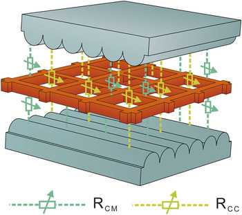
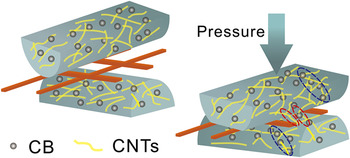
To elucidate the working principles of our multilayered piezoresistive sensor for wide-ranged pressure measurement, further investigation reveals that the sensor element operates mainly through the synergistic effects of the contact resistance mechanism and bulk resistance mechanism. To explain the mechanism of resistance variation more specifically, the total resistance can be expressed as R = R C + R CM + R CC, where R C denotes the bulk resistance of the CNTs/CB/SR composite films, R CM denotes the contact resistance between the composite films and the copper wire meshes, and R CC is the contact resistance between the adjacent composite films through the net holes of copper wire meshes (Fig. 7). In regard to the contact resistance mechanism, we attribute the significant decrease in resistance to the deformation of the semicylinder arrays on the surfaces of the composite films and the resulting variation in external contact area, which affects the contact resistance (R CM and R CC). As the applied pressure is increased, the large deformation of the semicylinder arrays produces a large increase in contact area (shown in Fig. 8, such as the part in the red dashed circles), which increases the conductive paths between the composite films and the copper wire meshes and those between the adjacent composite films through the net holes of copper wire meshes, resulting in the decrease of R CM and R CC. About bulk resistance mechanism, according to the conductive path theory, Reference Zhang, Dehghani-Sanij and Blackburn32 the increasing pressure makes the composite be compressed, which shortens the distance of conductive fillers (CNTs and CB), as a result, more conductive networks made up of CNTs/CB are built (shown in Fig. 8, such as the part in the blue dashed circles) and the bulk resistance R C becomes smaller gradually. Compared with the element of traditional monolayered structure which operates only through the bulk resistance mechanism, due to the wave-like surface of the sensitive material and the existence of copper wire meshes inserted between the adjacent sensitive material layers, the initial contact area becomes smaller, then the initial resistance of our sensor element becomes much higher and the resistance can keep varying significantly with the increasing pressure. When the applied pressure reaches to a certain value, the contact area hardly changes and no more new conductive paths emerge in the inner of the composite as the distance of conductive fillers hardly changes. In summary, by means of the synergistic effects of the contact resistance mechanism and bulk resistance mechanism, the multilayered piezoresistive sensor can detect the wide-ranged pressure with a high sensitivity.
Schematic of two kinds of contact resistance: R CM and R CC.

Schematic of deformation of the semicylinder arrays and variation of the contact resistance.

C. Influence of mesh number and thickness
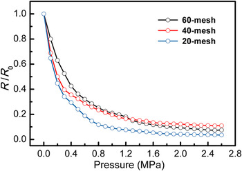
To further understand our multilayered piezoresistive sensor, the effects of mesh number of copper wire meshes and total thickness on this element were studied. As shown in Fig. 9, the element with copper wire meshes of 60-mesh is still sensitive to the applied pressure after 2.2 MPa, which has the widest workable pressure range. While the element with copper wire meshes of 20-mesh has the highest sensitivity according to the slope of the pressure response curve, especially in the low-pressure range. The reason is that the mesh number is higher that each net hole of copper wire meshes is smaller, then the contact area between the adjacent composite films through the net holes of copper wire meshes varies more slightly but more slowly with the pressure, so the resistance varies more slightly but keeps varying to a wider range of pressure.
Piezoresistivities of the sensor elements with copper wire meshes of three different mesh numbers.

In addition to the mesh number, the total thickness can also affect the performance of sensor element. Through the experimental research, the pressure measuring range of the element with thickness of 4, 5, and 6 mm (by changing the thickness of each composite layer, while the dimension of semicylindrical waves on the surfaces of composite layers remains unchanged) is 0–1.5, 0–1.8, and 0–2 MPa, respectively, which is mainly due to the bulk resistance (R C) variation of the composite films. The thicker composite films can be compressed by a greater pressure, meanwhile, the inner conductive network keeps varying so that the resistance changes with a wider ranged pressure.
D. Repeatability
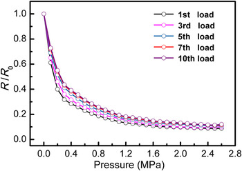
Finally, the sensor element (mesh number: 40, total thickness: 5 mm) underwent 10 consecutive electromechanical tests for repeatability assessment. The initial resistance under zero pressure (R 0) at test 1 is 58 kΩ and does not return to its original value in the previous runs since the irreversible breakage of fragile structures in the composite. After 5 runs, R 0 becomes constant (52 kΩ) with increasing runs. Figure 10 shows the pressure response curves of first, third, fifth, seventh, and tenth test. The result shows a quite difference between the first and the following tests, especially in the low-pressure range, which is due to the instability of the contact situation, the inner conductive network, and initial resistance under zero pressure (R 0). Then the piezoresistive behavior stabilizes after several loading runs (less than 10 runs), which proves that this multilayered piezoresistive sensor can work stably for pressure measurement.
The pressure response curves of the first, third, fifth, seventh, and tenth loading tests on the sensor element.

IV. CONCLUSIONS
In conclusion, a multilayered flexible piezoresistive sensor based on CNTs/CB/SR composite was designed and studied. Compared with the sensor element of traditional monolayered structure, the design of our sensor element was novel and found to be able to measure a wider range of applied pressure (0–1.8 MPa at least) with a higher sensitivity, which is due to the synergistic effects of the contact resistance mechanism and bulk resistance mechanism. Moreover, the influence of mesh number of copper wire meshes and total thickness on this element was also studied. Through consecutive loading tests, this sensor element showed a good reproducibility on pressure measurement. In the future, more influencing factors and optimization on the multilayered piezoresistive sensor will be further investigated to make this element be more suitable for flexible electronic skin devices.
ACKNOWLEDGMENTS
This work was financially supported by the Program of National Natural Science Foundation of China (Nos. 61401141, 61471155), Anhui Provincial Natural Science Foundation (No. 1508085QF115), and Research Development Funds of Hefei University of Technology (No. J2014HGXJ0087).