I. INTRODUCTION
Transparent conducting oxides (TCOs) have been widely used as transparent electrodes for flat panel displays including liquid crystal displays, organic light emitting diodes (OLEDs), and plasma displays. Among the several TCOs, tin-doped indium oxide (ITO) films are widely used due to their low electrical resistivity and high transparency in OLEDs and solar cells. As a degenerated semiconductor, ITO can be used as an antireflecting layer in n+-p optical sensors. Reference Haines and Bube1
ITO thin films can be prepared using a wide variety of techniques such as thermal evaporation, chemical vapor deposition, electron beam evaporation, sol–gel, pulsed laser deposition, magnetron sputtering, and spray pyrolysis. Reference Ginley, Hosono and Paine2 Some of the optoelectronic applications (solar cells, photoheterojunctions, and light emitting diodes on silicon) of thin ITO films, fabricated by spray pyrolysis, were reported in our earlier studies. Reference Malik, De la Hidalga-Wade, Zúñiga-Islas and Abundis-Patiño3–Reference Malik and De la Hidalga-Wade6
Transparent conducting ITO films have been also prepared by a direct current (DC) or radio frequency (RF) magnetron sputtering process using commercially available In2O3–SnO2 targets. Many studies show that postdeposition annealing is not essential when oxygen is added to the argon to improve the film stoichiometry, structural, and electro-optical properties of the films. However, the analysis of published results shows a considerable variation in the oxygen partial pressure to obtain the required film parameters. Commercial ceramic ITO targets usually are fabricated from a mix of high-purity In2O3 and SnO2 powders (90 wt%:10 wt%), according to the solubility limits of Sn in In2O3 (12.4–15 mol% SnO2), Reference Enoki, Echigoya and Suto7–Reference González, Mason, Okasinski, Buslaps and Honkimäki9 using hydrothermal processes at temperatures below 1500 °C. The key issues for obtaining high-quality ITO films are correct sintering techniques. X-ray diffraction (XRD) peaks, chemical composition, and the coloration of the ceramic target are principal characteristics to be optimized in the correct formation of the ITO target. However, to the extent of our knowledge, these important parameters are not provided by manufacturers. National Renewable Energy Laboratory (NREL) Reference Cessert, Voshida, Fesenmaier and Coutts15 and other researchers Reference Falk and Lakshmanan10 show that a thermal treatment in air or oxygen at 1300 °C leads to the formation of stoichiometry ITO targets having a light-green coloring similar to the color of mix of used powders, whereas a thermal treatment in reducing atmospheres (such as H2) results in a black coloring. Reference Cessert, Voshida, Fesenmaier and Coutts15 This specific color of the target can be due to the presence of undesirable phases as metallic tin and/or blue–black tin suboxide SnO due to the dissociative decomposition of SnO2 in SnO + 1/2 O2. The instable phase SnO can turn in Sn3O4 and pure Sn, whereas Sn3O4 will decompose in SnO2 and metallic Sn. It results in “black” color of the used target. That is why for receiving high-quality ITO films from commercially available targets, the oxygen additive is necessary.
If only argon is used as the working gas for the sputtering, the stoichiometry deviation of the commercial “black” target will be reproduced in the films leading to a low transparency and conductivity Reference Minami, Sonohara, Kakumu and Takata11–Reference Cessert, Voshida, Fesenmaier and Coutts15 of the films. Thus, the thermal history of the mixed powders is important since the powder characteristics after sintering are closely correlated with the target quality having a profound impact on the characteristics of sputtered thin layers. Reference Udawatte and Yanagisawa16
Whereas, it was shown Reference Nisha, Anusha, Antony, Manoj and Jayaraj17 that the ITO targets fabricated under laboratory conditions with sintering only in air atmosphere at 1300 °C, for 6 h present a light color close to the coloring of initial powders. The stoichiometry of In2O3 confirmed by XRD analysis allows fabrication of highly transparent ITO films in pure argon atmosphere without oxygen addition. Reference Nisha, Anusha, Antony, Manoj and Jayaraj17,Reference Nisha18 It is evident that sputtering in an argon atmosphere is more simple, better controllable than that in an argon–oxygen mixture. However, with commercial ITO targets because of their nonspecified (not controlled) SnO or metal (Sn) fractions, practical realization of this process to fabricate highly transparent and conductive ITO films presents some difficulties. After sputtering in Ar, the films should be annealed in air/oxygen atmosphere for obtaining optimal stoichiometry, high transparency, and conductivity.
For this study, the ITO films were deposited by means of DC magnetron sputtering with ITO “black” color targets fabricated by AJA Corporation with consequent thermal annealing in oxygen atmosphere at different temperatures. The crystallization structure, optical, and electrical properties, as well as the work function of the ITO films, were investigated and discussed.
II. EXPERIMENTAL PROCEDURE
ITO films were deposited on both “Corning 2947” glass and polyimide “Kapton” plastic substrates, using “AJA ATC Orion 5 UHV DC Magnetron Sputtering System” with 2 inch heads. The target to substrate distance was kept constant at 7.5 cm. Before the deposition, the substrates were cleaned in an ultrasonic bath with acetone, alcohol, and deionized water, and then dried using high-purity nitrogen. The system was evacuated to a base pressure of about 10−6 Torr prior to the film deposition. The argon (Ar) flow (12 sccm) was adjusted with an “MKS” mass flow controller, maintaining the working gas pressure at around 3 mTorr during the deposition. A power of 100 W was used for the film deposition process. The substrate was rotated to obtain film uniformity. Before the sputtering deposition, a presputtering was carried out for 10 min under the same conditions as the deposition. The substrate surface was not heated and maintained at a temperature lower than 50 °C. ITO films with a thickness of 200 ± 10 nm were grown. The films removed from the sputtering system were thermally annealed for 60 min under a constant flow of pure oxygen at temperatures in the range of 200–450 °C with a step of 50 °C.
The structural characterization of the ITO films was carried out using a “Bruker D8 Advanced X-ray Diffractometer,” with Cu Kα radiation (λ = 0.15406 nm). The morphological features of the ITO films were examined using the Ambios USPM atomic force microscope (AFM). The Keithley's Series 2400 Source Measurement Unit (Keithley Instruments, Inc., Cleveland, OH) and the Ecopia HMS-5000 Hall Effect Measurement System (Bridge Technology, Chandler Heights, AZ) were used for electrical characterization. Optical measurements were carried out in the 400–1100 nm wave length range using a F20 Filmetrics spectrometer (Filmetrics, Inc., San Diego, CA).
III. RESULTS AND DISCUSSION
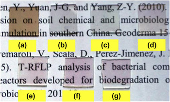
Our analysis of the XRD patterns demonstrates that the as-deposited ITO films grown at room temperature were amorphous. Visual “black” color of the films is changed after annealing in the oxygen as shown in Fig. 1. Dark color of the films at annealing temperature below 250 °C can be explained by the presence of nonstoichiometric amorphous inclusions as tin suboxide or metallic tin inside the deposited films.
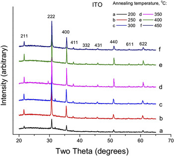
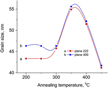
When the annealing temperature exceeds 200 °C, the crystallization process takes place. The availability of oxygen at the annealing process improves the film stoichiometry, increasing the transparency, the grain size, and conductivity. All peaks in XRD spectra following the ASTM standard, intensity of the peaks (Fig. 2), and preferred (222) orientation for annealed films do not show a significant change for all annealing temperatures above 200 °C. The average (222)/(400) peak intensity ratio has a value of 2. The grain size for the (222) and (400) planes (Fig. 3) has been estimated from XRD spectra using a well-known Scherrer–Bragg equation. The results obtained demonstrate that the grain sizes increase with the enhancement in the annealing temperature up to 350 °C beyond which the crystalline size values start to slightly reduce. The largest grain size (55 nm) is obtained for the ITO sample annealed at 350 °C. These samples have the optimal dimension and connectivity between grains reducing area of grain boundaries, and consequently recombination rate at the grain boundaries.
Color of the ITO films after a heat treatment at different temperatures in oxygen: (a) 200 °C, (b) 250 °C, (c) 300 °C, (d) 350 °C, (e) 400 °C, and (f) 450 °C. The differences in color are due to an interference effect.

XRD patterns of the ITO films annealed at different temperatures.

Grain size of the ITO films deposited on the Corning 2947 glass substrate for (222) and (400) planes.

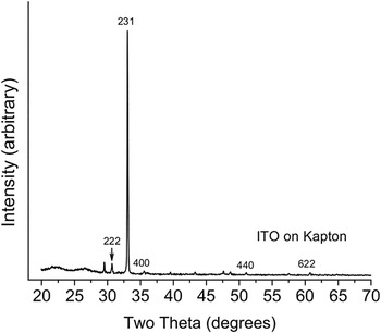
The XRD spectra of the ITO films deposited on a polyimide substrate (Fig. 4) show unexpected results such as a strong grain orientation in the (231) plane. With this experiment, we only want to show the application of a proposed method for the same type of flexible substrates, such as polyimide. At present, we do not know the reason for the (231) texture, but this is the reliable experimental result.
XRD patterns for ITO films on Kapton polyimide substrates after a 300 °C annealing process in oxygen atmosphere.

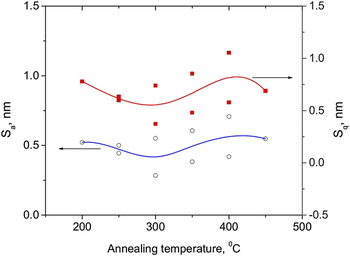
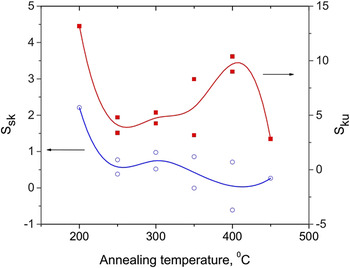
The average roughness (S a), root means square (RMS) roughness (S q), skewness (S sk), and kurtosis (S ku) were determined from the analysis of AFM images as shown in Figs. 5 and 6. The minimal average roughness and RMS roughness values, 0.41 and 1.06 nm, respectively, correspond to the annealing temperature of 300 °C. For the skewness and kurtosis parameters, it is observed that for annealing temperatures of 400–450 °C, the values of S sk have an average value close to zero corresponding to a symmetrical height distribution on the film surface. At lower annealing temperatures, the S sk values become positive, indicating that the surface morphology is determined by peaks rather than valleys. The S ku values for annealing temperatures of 200–400 °C are above 3, which indicate that dominating peaks are rather smooth. Annealing influences on surface morphology and electrical characteristics of multilayered structures, which can be deposited on the ITO film. Our AFM parameters confirm sufficiently plane surface of the films. No correlation of them with electrical parameters was observed.
AFM roughness parameters S a and S q of the ITO films deposited on the Corning 2947 glass substrate.

AFM roughness parameters S sk and S ku of the ITO film deposited on the Corning 2947 glass substrate.

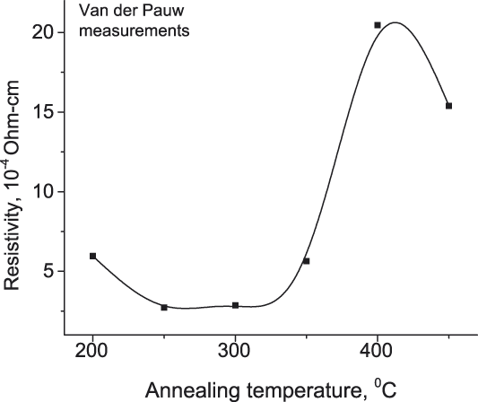
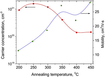
The resistivity of the ITO films after heat treatment in oxygen at temperatures of 200–450 °C is shown in Fig. 7. It can be seen that the resistivity is affected severally by the annealing temperature. It decreases for an increasing annealing temperature and presents a minimum at 250–325 °C. Further increment in temperature leads to a sharp increase in resistivity. For increasing annealing temperature, the carrier concentration presents a maximum as shown in Fig. 8 around the same temperature range where the resistivity of the film presents its minimum. The Hall mobility increases monotonically with the growing temperature. The carrier concentrations in the films annealed at 400 and 450 °C did not change (Fig. 8), but the mobility also shown in the same figure has enhancement. As specific resistance is inversely proportional to these values, it decreases as observed in Fig. 7.
Resistivity of the ITO films after a heat treatment in oxygen at temperatures of 200–450 °C.

Carrier concentration and Hall mobility of the ITO films after the thermal treatment in oxygen at temperatures in the 200–450 °C range.

Two factors determine the conductivity and carrier concentration in the ITO films: doping by tin atoms that substitute a part of indium atoms and the oxygen vacancies. Increasing temperature leads to an increase of the conductivity and carrier concentration due to the activation of the tin atoms. However, further temperature increase for annealing in oxygen leads to a reduction of oxygen vacancies, resulting in a reduction of both carrier concentration and conductivity. The increase of the carrier mobility for an increasing annealing temperature is connected with the growth of the grains and an improved structural morphology of the film.
The electrical parameters of 215-nm thick ITO films deposited on Kapton substrates at room temperature show the best results after annealing in oxygen atmosphere for 1 h: resistivity ρ = 3.2 × 10⁻⁴ Ohm cm, carrier concentration n = 1.4 × 1021 cm−3, and mobility μ = 13.7 cm2/V s.
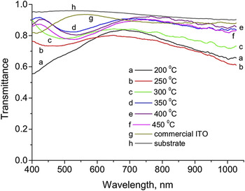
Figure 9 shows the optical transmittance spectral measurements of the ITO films deposited on Corning 2947 glass substrates and annealed at different temperatures in oxygen ambient atmosphere. It can be seen that the annealing in oxygen significantly improves the transmittance for annealing temperatures above 300 °C. This effect can also be clearly seen from visual observation (Fig. 1) because the annealing improves the film stoichiometry.
The optical transmittance spectral measurements of the ITO films deposited on Corning 2947 glass substrates and annealed at different temperatures in oxygen ambient atmosphere.

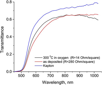
The transmittance of the ITO film deposited on “Kapton” substrates before and after annealing in oxygen at 300 °C for 1 h is shown in Fig. 10.
Transmittance of the ITO film deposited on the Kapton substrate and annealed in oxygen at 300 °C for 1 h.

Here, it is relevant to use the results published by Minami et al. Reference Minami, Sonohara, Kakumu and Takata11 They deposited the ITO films on flexible and glass substrates by DC planar magnetron sputtering in argon without addition of the oxygen using the ITO targets sintered from In2O3 with different contents of SnO2 powders (0, 1, 5, and 10 wt%) at 1000 °C for 5 h in air with the next heat treatment at 800 °C for 5 h in an Ar + H2 (10%) gas atmosphere. The as-deposited ITO films on both substrates have low transparency (Figs. 1 and 5 in Ref. Reference Minami, Sonohara, Kakumu and Takata11) due to the presence S(II)O suboxide having dark color that was present in sintered targets. Darkness of the films increases with SnO2 content in the target. It is not happened for the In2O3 films deposited from the target containing 0 wt% of Sn. Only after annealing of the ITO film with different SnO2 contents, all ITO films became transparent and highly conductive. It may confirm our assumption about the presence of tin suboxide in commercially available “black” ITO targets.
For practical applications, the electrical conductivity and optical transparency of ITO films should exceed certain minimum value. Ideally, these two parameters should be as high as possible. However, the simultaneous performance of maximum transmission and conductivity is not possible to achieve in most cases.
Haacke Reference Haacke19 proposed the figure of merit ϕTC, which is possible to calculate for films with different thicknesses and fabrication history, and provides a better balance between the transmittance T and sheet resistance R s of the film:
 $${\phi _{{\rm{TC}}}} = {{{T^{10}}} \over {{R_{\rm{s}}}}}\quad .$$
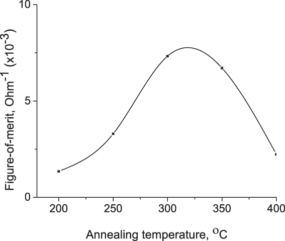
Figure 12 shows the figure of merit for the ITO films annealed at different temperatures in oxygen atmosphere. In Fig. 11, the maximum ϕTC is observed for the films after postannealing in oxygen at 325 °C.
Figure of merit calculated at a wave length of 700 nm for the ITO films annealed at different temperatures in oxygen atmosphere.

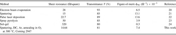
In Table I, we present a comparison of the figure of merit obtained in this work with values reported for ITO films fabricated using different techniques.
Comparison of the figure of merit obtained in this work with values reported for ITO films fabricated using different techniques.

Since ITO films exhibit high light transmission characteristics in the visible region and a high electrical conductivity, they are widely used in optoelectronics applications such as solar cells, liquid crystal flat panel displays, and a hole injecting electrode in OLEDs. In many of such applications, the work function of ITO has a critical importance in the device performance because it affects the energy barrier height at the heterojunction interface. The published values of the ITO work function lie in the 4.1–4.7 eV range. Reference Shewchun, Dubow, Wilmsen, Singh, Burk and Wager25–Reference Schlaf, Murata and Kafafi29 A value of 5.53 eV has also been published. Reference Ishida, Kobayashi and Nakato30
Since the work function depends on the fabrication technique, one can see a large difference between reported results. Usually, the ITO films sputtered in argon–oxygen atmosphere have a low value of the work function that influences on efficiency optoelectronic devices using these films as transparent conducting electrodes. A high value of the work function (above 5 eV) has been obtained after the treatment of commercial ITO films in O2 and ozone plasma. Reference Schlaf, Murata and Kafafi29,Reference Ishida, Kobayashi and Nakato30 This work function is determined from ultraviolet photoemission spectroscopy measurements in an ultrahigh vacuum (UHV) apparatus. Reference Park, Choong and Gao28,Reference Schlaf, Murata and Kafafi29 However, such increasing work function has superficial effect and is applicable to thin film multilayered structures deposited on the ITO layer.
For the estimation of the work function of annealed ITO films in this work, we use a well-known method based on a capacitance–voltage (C–V) measurement of two capacitors, fabricated under the same conditions on a silicon substrate covered by a SiO2 layer and using Al and ITO gates. Reference Nicollian and Brews31 The work function of Al is known in the literature as 4.15 eV. To estimate the work function of annealed ITO films, we fabricated metal oxide semiconductor (MOS) capacitors under the same conditions with Al and ITO gates. The flat band shift of such capacitors allows making conclusions about the work function of the ITO films annealed at different temperatures.
Here one important question arises. Do we think that the work function of our ITO films, deposited under the same conditions on different substrates (Corning glass and thermally grown SiO2), and annealed in an O2 atmosphere, is the same? This is a simple speculation.
The chemical content of SiO2 in the used Corning glass 2947 substrate (amorphous structure) is around 60%. The SiO2 layer thermally grown on the silicon substrate also presents an amorphous structure. Based on the coincidence of sheet resistance measurements of the annealed oxygen ITO films deposited on Corning glass substrates and on thermally grown SiO2 layer on the silicon, we are assuming that it is possible to use the capacitance method for the estimation and monitoring of the ITO work function.
MOS capacitors were fabricated on n-type 3–5 Ω cm silicon wafer. The SiO2 layer, with a thickness around 70 nm, was grown at 1000 °C. Then, the wafer was cut into two parts for the fabrication of the capacitors, one with Al and the other with the ITO gate. An Al layer was deposited at the back for electrical contact. A postannealing in forming gas was applied to the half wafer with the Al–SiO2–Si–Al structures.
The ITO layer was deposited by sputtering on the other half wafer with the SiO2–Si structure and Al back-contact after the thermal treatment of this sample, together with the Al–SiO2–Si–Al sample in the forming gas.
The sample with ITO–SiO2–Si–Al was divided into several parts for annealing in an oxygen atmosphere at different temperatures. A photolithography process was applied for etching the Al and ITO layers to obtain the MOS capacitors. Since the thermal processes used for growing the SiO2 and annealing in the forming gas are the same for both half wafers, we assume that the positive charge at the SiO2–Si interface is also the same.
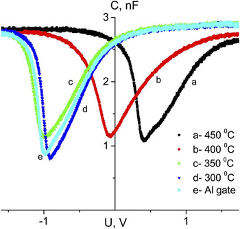
Figure 12 shows a comparison of the quasi-static characteristics of the Al–SiO2–Si capacitors with those obtained for the ITO–SiO2–Si capacitors, where the ITO gate was annealed at different temperatures. The difference between the flat band voltages of the two types of capacitors allows for the estimation of the work function of the ITO films annealed at different temperatures in an oxygen atmosphere. The films annealed at 300 and 350 °C present a work function very close to that of Al. The work function value for Al is conventionally accepted as 4.15 eV, Reference Nicollian and Brews31 which was used here for the calculation of work function for ITO from shift of the flat band values in C–V characteristics (see Fig. 12). However, the films annealed at 400 and 450 °C present a high value of work function, 4.99 and 5.48 eV, respectively. Such an increase of the work function at high annealing temperature cannot be explained in terms of the shift of the Fermi level to a lower energy in the conduction band because of decreasing carrier density in highly degenerated ITO films. The calculated value of such shift for the films annealed at high temperatures is close to 0.5 eV, if the reduced effective mass of electrons in the ITO films is supposed to be 0.5 m0. Reference Sato, Tokumaru, Nishimura, Song and Shigesato32
Quasi-static C–V characteristics of the Al–SiO2–Si capacitor (e) in comparison with the characteristics of ITO–SiO2–Si capacitors (the ITO gate was annealed at different temperatures: (a) 450 °C, (b) 400 °C, (c) 350 °C, and (d) 300 °C).

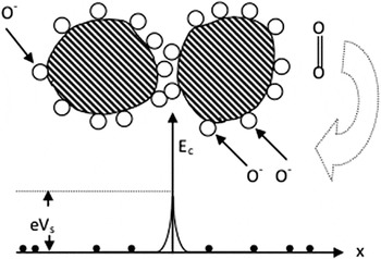
The experimental values of the work function obtained for the films annealed at high temperatures can be explained considering the oxygen absorbed on the grain boundary inside the ITO films. At low temperatures, this is physical absorption, whereas at high temperatures a chemical adsorption takes place Reference Schmid33 ; namely, at temperatures above 350 °C, the oxygen molecule adsorbed on the film grains dissociates into oxygen atoms, which take one conduction electron each from the ITO to form oxygen negative ions, thus the oxygen becomes bounded to the grains by electrons. The presence of negatively charged oxygen ions produces a band-bending eVs at the grain's surface and induces changes in a space charge region in the semiconductor and consequently shifts of the flat band value, which is reflected in the values for the effective work function of the ITO film (Fig. 13).
Schematic representation of the surface potential eVs at the two-grain boundaries due to chemisorbed oxygen atoms.

Taking into account high electron concentration in the ITO films, a significant amount of electrons have the possibility to cross this potential barrier at the barrier “tip” without changing in the film conductivity. The observed shift of flat band voltage and consequent change of effective work function of ITO films provides reliable values rather than absolute values for work function, which are calculated for the accepted value of 4.15 eV for Al reference electrode.
The results obtained in this work allow the possibility of tuning the value of the ITO work function by changing the post-annealing temperature in oxygen atmosphere. Such tuning is important for the design of optoelectronic devices presenting high-level parameters. Note that the modification of the work function described in this work is due to effects occurring in the volume of the ITO films. This approach of the work function modification significantly differs from the surface work function modification due to plasma treatment, Reference Low, Zhu, Zhang and Chua34 UV-ozone treatment, Reference Song, So, Wang, Qiu and Cao35 chloroform solution treatment, Reference Helander, Wang, Qiu, Greiner, Puzzo, Liu and Lu36 and KMnO4 solution treatment Reference Yang, Zhao, Xu, Zhang, Yan, Kong, Fan, Zhang and Xu37 of the ITO films having superficial changing of the work function.
IV. CONCLUSIONS
In this work, we present the results on characteristics of ITO films deposited by DC magnetron sputtering with commercial ITO targets from “AJA Inc.” on Corning 2947 glass substrates, in argon environment with following annealing in oxygen atmosphere. This fabrication is better controllable and reproducible in comparison with sputtering with commercially available ITO targets in a mixed Ar + O2 atmosphere.
It has been shown that to obtain a stoichiometric high conductive and transparent ITO film with a nanocrystalline structure, deposited by sputtering of the commercial ITO target used in this work, a postannealing of the films in oxygen environment is required. The lower value of the resistivity around 3 × 10⁻⁴ Ω cm and the higher value of the figure of merit of 7.4 × 10⁻³ Ω−1 for 200 nm thick films are obtained after postannealing the films in oxygen atmosphere at 300 °C for 1 h.
It was observed that postannealing treatment in oxygen allowed for the tuning of the work function of the ITO films in the 4.2–5.5 eV range, depending on the treatment temperature. The tuning of work function for TCO and, in particular, for ITO films is of principal importance for applications in many optoelectronic devices.
The fabrication method reported in this study allows the fabrication of ITO films with high electro-optical parameters on flexible polyimide substrates.
ACKNOWLEDGMENTS
This work was partially supported by CONACyT-Mexico under Grant No. 102397. Authors acknowledge the technical staff at the Microelectronics Laboratory INAOE and Dr. A. Kosarev (INAOE) for constructive discussions.