I. INTRODUCTION
Bismuth antimony telluride (BiSbTe) thermoelectric alloys, which are possibly the only thermoelectric materials suitable for use at near room temperature, have great application potential for cooling, heating, and power generation.Reference Goldsmid and Douglas1 Thermoelectric solid state cooling can enable next-generation cooling with higher efficiency to replace vapor-compression refrigeration/air-conditioning, and thermoelectric power generation can be utilized for low-grade waste heat harvesting to improve power efficiency in many industries including the automotive sector. However, applications remain constrained by the need for higher efficiency thermoelectric materials, characterized by a high dimensionless figure of merit (ZT); ZT = (S 2σ/κ)T, where S, σ, κ, and T are Seebeck coefficient, electrical conductivity, thermal conductivity, and absolute temperature, respectively. To increase ZT, a large S, high σ, and low κ are essential. ZT of commercial BiSbTe bulk alloys has remained at around 1 for the past half-century. Emergence of high-ZT thermoelectric materials is highly demended to widen the thermoelectric application area.
Recent efforts to enhance ZT in BiSbTe bulk alloys have focused on reduction of the lattice thermal conductivity κlatt without severe reduction of associated electrical conductivity σ through a phonon glass electron crystal approach by developing homogeneous or heterogeneous nanostructures.Reference Venkatasubramanian, Siivola, Colpitts and O’Quinn2–Reference Slack and Rowe9 Poudel et al. obtained a maximum ZT of 1.4 at 373 K by reducing κlatt to 0.35–0.4 W/(m K) in nanocrystalline BixSb2−xTe3 bulk alloys with high-density grain boundaries.Reference Poudel, Hao, Ma, Lan, Minnich, Yu, Yan, Wang, Muto, Vashaee, Chen, Liu, Dresslhaus, Chen and Ren10 Cao et al. developed bismuth telluride (Bi2Te3)/antimony telluride (Sb2Te3) bulk nanocomposites using hydrothermal synthesis and hot pressing, achieving a maximum ZT of 1.47 at 438 K.Reference Cao, Zhao, Zhu, Zhang and Tu11 Very recently, Fan et al. reported a record high ZT of 1.80 at 316 K in Bi0.4Sb1.6Te3,Reference Fan, Zhao, Guo, Yan, Ma and Hng12 attained by exploiting nanoinclusions obtained through rapid solidification involving melt spinning. Solution-based bottom-up production of various forms of (Bi,Sb)2(Te, selenium (Se))3 nanophases has been attempted very recently for nanocomposites with high-density grain boundaries by bottom-up approach for possible mass production.Reference Scheele, Oeschler, Meier, Kornowski, Klinke and Weller13–Reference Mehta, Zhang, Karthik, Singh, Siegel, Borca-Tasciuc and Ramanath19 Forming phase boundaries by adding high-density nanosized second phase is another way to reduce κlatt.Reference Liu, Li, Chen and Zhang20, Reference Lee, Kim, Kim, Lee, Lee, Rhyee, Jung, Kim, Wang and Koumoto21
On the other hand, few approaches for increasing the value of Seebeck coefficient (S) in BiSbTe-based thermoelectric alloys have been presented. In lead telluride (PbTe)-based thermoelectric alloys, S was substantially enhanced by thallium (Tl)-doping, which increases the density of states (DOS) of the valence band over a narrow energy range near the Fermi energy level due to the formation of a resonance state.Reference Heremans, Jovovic, Toberer, Saramat, Kurosaki, Charoenphakdee, Yamanaka and Snyder22 Jaworski et al. suggested tin (Sn) doping as a means of enhancing S in Bi2Te3 alloys through the provision of an excess DOS near the valence band edge.Reference Jaworski, Kulbachinskii and Heremans23 They also provided experimental proof of S enhancement by resonant state formation in Sn-doped Bi2Te3. Faleev and Léonard suggested that S enhancement can also be attained by a carrier energy filtering effect, that is, a strong energy dependence of the carrier relaxation time caused by band bending at the heterointerface between metallic inclusions and thermoelectric host materials.Reference Faleev and Léonard24 They presented a theoretical model and numerical calculations of the enhancement of S in a PbTe composite including lead (Pb) nanoinclusions. Experimental evidence of S enhancement has also been reported in various thermoelectric nanocomposites, including indium gallium arsenide/erbium arsenide (In0.53Ga0.47As/ErAs) nanocomposite,Reference Zide, Klenov, Stemmer, Gossard, Zeng, Bowers, Vashaee and Shakouri25 lead telluride/lead (PbTe/Pb) nanocomposite,Reference Heremans, Thrush and Morelli26 ytterbium-doped cobalt antimonide/gallium antimonide (Yb0.26Co4Sb12)/(GaSb) nanocomposite,Reference Xiong, Chen, Huang, Bai and Chen27 and (titanium, zirconium, hafnium) (cobalt, nickel) antimonide/indium antimonide [(Ti,Zr,Hf)(Co,Ni)Sb/InSb] nanocomposite.Reference Xie, He, Zhu, Su, Wang, Holgate, Graff, Ponnambalam, Poon, Tang, Zhang and Tritt28 However, no direct observation of the carrier energy filtering effect has thus far been made in Bi2Te3 alloys. Very recently, Ko et al. presented experimental results demonstrating an enhanced S by embedding platinum (Pt) nanoparticles in Sb2Te3.Reference Ko, Kang and Murray29
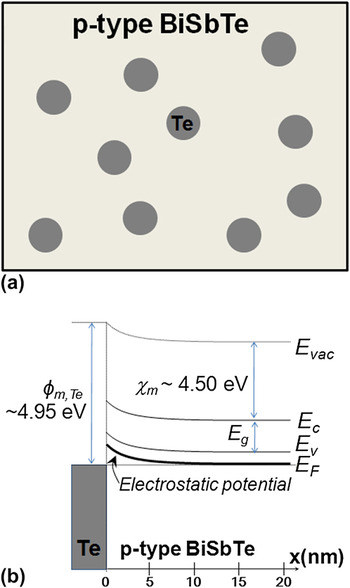
Based on the concept of band bending at heterointerfaces as a carrier energy filter, we present experimental evidence of a carrier energy filtering effect and enhanced phonon scattering in Te nanoparticle-dispersed Bi0.5Sb1.5Te3 films. The main concept, which involves a BiSbTe matrix with Te inclusions, is illustrated in this article in Fig. 1. In this case, carrier transfer induces band bending away from the heterointerfaces between the BiSbTe matrix and Te nanoparticles, as shown in the sample energy diagram for an interface presented in Fig. 1(b) (the electron affinity χm and band gap E g of p-type BiSbTe alloys is around 4.50 and 0.2 eV, respectively, and the work function of Te, φm,Te = 4.95 eV). The presence of the electrostatic potential causes energy-dependent scattering of carriers.Reference Faleev and Léonard24 The initial results have been published previously briefly.Reference Kim, Ahn, Yeon, Hwang, Kim, Lee and Lee30 In this article, we present more detailed experimental data and discussion. In addition, the effect on the thermal conductivity of the embedded Te nanoparticles was explored to confirm the possible effective scattering of phonons. Thus, the primary objectives of this work are to provide a thermoelectric characterization of Te-nanoparticle-embedded BiSbTe alloys experimentally and to explain the effect of Te nanoparticles on thermoelectric properties based on the relaxation time calculation. The secondary objective is to confirm that the high-density embedded nanoparticle reduces thermal conductivity, and thereby verify the beneficial effects of Te nanoparticles on thermoelectric performance or ZT.
(a) Schematic illustration of the BiSbTe thermoelectric semiconductor matrix with embedded high density Te nanoparticles. (b) A sample of a schematic energy diagram at the heterointerfaces between p-type BiSbTe and Te nanoparticles at 300 K for work function φm of Te = 4.95 eV, P = 7.0 × 1019 cm−3, electron affinity χmof p-type BiSbTe ∼4.50 eV, and barrier potential ∼0.25 eV. Barrier potentials may form near the interface, and low energy carriers scatter strongly due to the barrier potential. The depletion width is ∼5 nm in this case.

As the amount of nanosized Te particles is increased up to 15 vol%, S increased rather significantly. Even though σ was reduced moderately, the overall thermoelectric power factor (S 2σ) was increased by more than 40%. The results are discussed based on the theoretical model for the carrier energy filtering effect in thermoelectric materials with nanoinclusions proposed by Faleev and Léonard.Reference Faleev and Léonard24 In addition, we confirmed that the nanoparticle-embedded films exhibited reduced thermal conductivities, permitting further enhancement of the thermoelectric figure of merit ZT. The advantages of Te nanoinclusions in p-type Bi0.5Sb1.5Te3alloys on thermoelectric performance are experimentally realized by both electron- and phonon scattering.
II. EXPERIMENTAL DETAILS
First, a control Bi0.5Sb1.5Te3 film was deposited up to a thickness of 500 nm by using pulsed laser deposition (PLD) on a magnesium oxide (MgO) substrate. The deposition was performed at a substrate temperature of 125 °C in a 200 mTorr argon (Ar) atmosphere with a krypton fluoride (KrF) excimer laser fluence of 2.0 J/cm2 on a MgO substrate, and the deposited films were annealed at 225 °C for 2 h in an Ar atmosphere. A 2-inch diameter Bi0.5Sb1.5Te3 target was prepared by spark plasma sintering (SPS) under 70 MPa at 480 °C for 3 min, whereas the Bi0.5Sb1.5Te3 powders were prepared with a melt process; high-purity (>99.999%) Bi, Sb, and Te granules were weighed according to the composition Bi0.5Sb1.5Te3and loaded into a vacuum-sealed quartz tube of 10 mm, and the contents were melted and homogeneously mixed in a rocking furnace for 10 h at 1073 K.
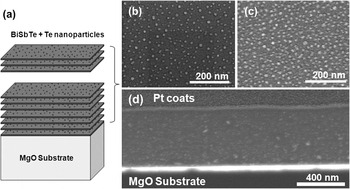
Figure 2(a) illustrates the process for preparing BiSbTe/Te composite films by an alternate deposition technique; Te particles of 10–20 nm size were introduced by growth of alternating multilayers of ultrathin Te and Bi0.5Sb1.5Te3. The deposition was performed at a substrate temperature of 125 °C in a 200 mTorr Ar atmosphere with a KrF excimer laser fluence of 2.0 J/cm2 on a MgO (100) substrate (5.0 mm × 10.0 mm wide, and 0.5 mm thick), and the deposited films were annealed at 225 °C for 2 h in an Ar atmosphere. The deposition of Te equivalent to a 0.5 nm thick film (6 pulses with a laser fluence of 2.0 J/cm2) produced a layer of Te nanoparticles with sizes of 10–20 nm at a lateral density of ∼300 μm−2, as shown in Fig. 2(b). The average lateral distance between Te nanoparticles is calculated as ∼40–50 nm. For producing Te-nanoparticle-embedded film samples with nominal volume fractions of 2.5%, 5%, 6%, 7.5%, 10%, and 15%, alternate deposition of Te nanoparticles and Bi0.5Sb1.5Te3 layers of 20, 10, 8.3, 6.7, 5, and 3.3 nm thicknesses was repeated 25, 50, 60, 75, 100, and 150 times, respectively. As a result, the total nominal thicknesses of the samples were 513, 525, 530, 538, 550, and 575 nm (the sum of the thicknesses of all the Bi0.5Sb1.5Te3layers remains at a constant value of 500 nm).
(a) Schematic illustration of the alternate deposition of Te nanoparticles and Bi0.5Sb1.5Te3 layers. (b) Plan-view secondary electron image of Te nanoparticles deposited on Bi0.5Sb1.5Te3 layers. Te particle layer equivalent to a 0.5-nm thick continuous film (6 pulses of laser). (c) Plan-view secondary electron image of Te nanoparticles deposited on Bi0.5Sb1.5Te3layers. Te particle layer equivalent to a 0.75-nm thick continuous film (9 pulses of laser). (d) Cross-sectional secondary electron image (Focused ion beam cut) of the 7.5% Te addition film.

A second set of Bi0.5Sb1.5Te3/Te composite films were prepared with higher lateral density of Te particles equivalent to a 0.75-nm thick film (9 pulses with a laser fluence of 2.0 J/cm2). As shown in Fig. 2(c), the lateral density of the Te particles was increased to ∼450 μm−2. Samples with nominal Te volume fractions of 3%, 6%, and 9% were prepared by alternate deposition of Te nanoparticles and Bi0.5Sb1.5Te3 layers of 25, 12.5, and 8.3 nm thicknesses repeated 20, 40, and 60 times, respectively. As a result, the total nominal thicknesses of the samples were 515, 530, and 545 nm. In this case, the deposition was performed at a substrate temperature of 225 °C in a 200 mTorr Ar atmosphere with a KrF excimer laser fluence of 2.0 J/cm2, and the deposited films were annealed at 225 °C for 2 h in an Ar atmosphere. Figure 2(d) exhibits a focused ion beam cross-section secondary electron image of the 7.5 vol% Te addition film, revealing a relatively homogeneous dispersion of Te nanoinclusions in the direction normal (i.e., vertical) to the film surface.
The composition analysis was performed by energy-dispersive spectroscopy (EDS, 7200-H, Horiba, Edison, NJ) on the scanning electron microscope operating at <20 kV. The composition (atomic percent) of the nanoinclusion-free Bi0.5Sb1.5Te3films was measured as Bi-9.9%, Sb-29.1%, Te-61.0%, whereas the composition of the target was measured as Bi-9.3%, Sb-29.7%, Te-61.0%. It can be concluded that there was no difference between the compositions of the film and the target. In fact, PLD is typically known to provide good congruent transfer of target composition to film in the regime of ablation. Since the deposition parameters had been maintained throughout the deposition process, the composition of the films was expected to be uniform though film thickness.
The in-plane σ and S were measured simultaneously from 320 K to 520 K by a four-point probe method using a ZEM-3 (ULVAC-RIKO, Kanagawa, Japan). In this case, thin film measurements were made successfully by the ZEM-3 apparatus by using thin-film measuring attachment, which provides secure electrical contact of the surface of the film and electrode. The measuring attachment includes two 25-μm thick Ni plates fixed with silver paste on the both side of the thin film specimen located on the alumina ceramic corner pillar. Hall measurements were performed at room temperature in a Lakeshore Hall effect measurement system (HMS). The effective carrier concentration (n eff) was estimated by the one-band model using n eff = −1/(R He) and σ = n effeμHall, where R H and e are the Hall coefficient (R H = ρxy/B) and elementary charge of the electrons (e = 1.602 × 10¹⁹ C), respectively. The MgO substrate is nonconductive, and thus it should not affect measurement of σ, S, and carrier density. After the measurements, thin layer of gold was deposited for the thermal conductivity measurement based on a 2ω method. Thermal conductivities κ were measured in the direction normal (i.e., vertical) to the film surface by a ULVAC-Riko TCN-2ω (ULVAC-RIKO, Kanagawa, Japan) thermal conductivity measurement system. The measurement was done at room temperature in a vacuum. An AC sinusoidal signal was applied across the gold film to supply heating. The AC frequency was varied from 200 to 10,000 Hz.
III. RESULTS AND DISCUSSION
A. Enhancement of the Seebeck coefficient and power factor
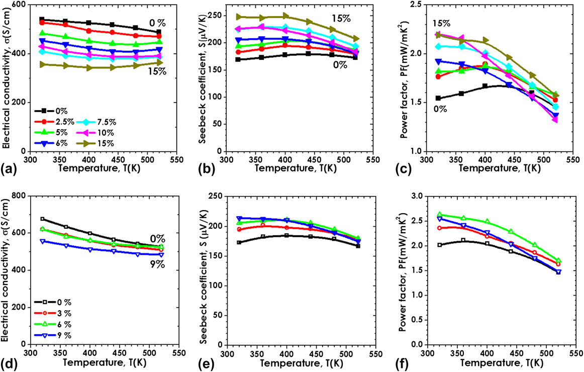
Figures 3(a)–3(c) exhibit the temperature dependence of σ, S, and the power factor values of the Te-nanoparticle-embedded Bi0.5Sb1.5Te3 and nanoinclusion-free Bi0.5Sb1.5Te3 films as functions of the measured temperature of the first sample set I. σ decreases systematically with increasing density of Te nanoparticles throughout the measured temperature range of 320–520 K, as shown in Fig. 3(a). Figure 3(b) shows a large S enhancement for all the Te-embedded films compared with the nanoinclusion-free Bi0.5Sb1.5Te3 film. The power factor increases as the Te inclusion density increases. Figures 3(d)–3(f) exhibit σ, S, and the power factor values of the second sample set II with Te contents of 3%, 6%, and 9%. σ decreases with increasing density of Te nanoparticles throughout the measured temperature range of 320–520 K [Fig. 3(d)]. Figure 3(e) shows a S enhancement for all the Te-embedded films compared with the nanoinclusion-free Bi0.5Sb1.5Te3film. The power factor increases as the Te-inclusion density increases.
(a, d) σ, (b, e) S, and (c, f) thermoelectric power factor values of Te-nanoparticle-embedded Bi0.5Sb1.5Te3 and nanoinclusion-free Bi0.5Sb1.5Te3films as functions of the temperature of sample sets I and II.
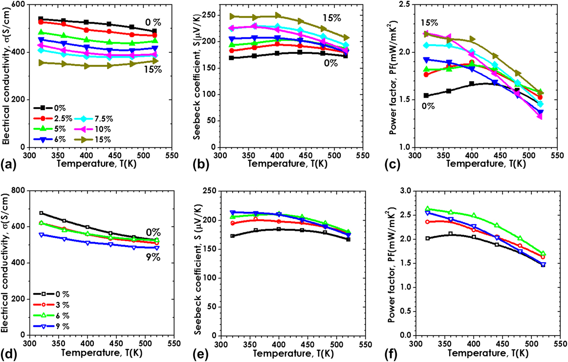
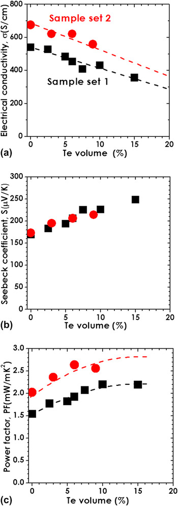
Figure 4(a) shows σ values at 320 K of the first and second sample sets measured by a 4-probe (ULVAC-RIKO ZEM-3, squares), with both showing linear decreases as the Te-nanoinclusion density increases. σ decreased linearly from 540 to 356 S/cm and from 680 to 600 S/cm for sample sets I and II, respectively. To examine the carrier filtering effect, we evaluated the effective carrier concentration (n eff). The measured effective carrier concentrations were 7.5, 5.5, 4.8, 4.4, 3.7, 4.1, and 4.4 × 1019 cm−3 for the samples with Te addition of 0%, 2.5%, 5%, 6%, 7.5%, 10%, and 15%, respectively. For the second sample set, the measured effective carrier concentrations were 6.9, 6.6, 5.1, and 5.0 × 1019 cm−3 for the samples with 0%, 3%, 6%, and 9% Te, respectively. The addition of Te nanoparticles enhances the electron scattering by the carrier energy filtering effect due to the barrier potential formed by the Te/Bi0.5Sb1.5Te3 heterointerfaces.Reference Faleev and Léonard24 Consequently, the effective carrier concentration is reduced as the amount of Te addition increases. However, in the case of large Te addition exceeding ∼10%, the barrier potentials may become overlapped due to very short distances between the nanoinclusions, and therefore the carrier concentration may be increased. The S value of the 15 vol% addition films increased significantly from 169 to 248 μV/K at 320 K compared with the nanoinclusion-free Bi0.5Sb1.5Te3 film [Fig. 4(b)]. Consequently, the power factor increased significantly, as shown in Fig. 4(c).
(a) σ, (b) S, and (c) power factor at 320 K with the Te nanoinclusion density.

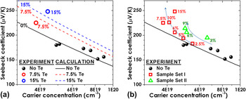
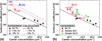
Figures 5(a) and 5(b) shows S as a function of the carrier concentration (so-called Pisarenko plot) at room temperature. In Fig. 5(a), closed circles represent the Pisarenko relationship of the nanoinclusion-free Bi0.5Sb1.5Te3 films. Nanoinclusion-free Bi0.5Sb1.5Te3 films were prepared under different deposition and annealing conditions for producing data points at several different carrier concentrations. The solid line represents the calculated room-temperature S (i.e., the Seebeck coefficient S at room-temperature) as a function of the carrier concentration of nanoinclusion-free Bi0.5Sb1.5Te3 samples based on the relaxation-time models.Reference Faleev and Léonard24 Here, we used the following parameters for Bi0.5Sb1.5Te3 from literaturesReference Huang and Kaviany31, Reference Zhou, Li, Ghen and Yang32: E g = 0.13 to 1.08 × 10⁻⁴ T (eV), m * = 0.06m e, ε0 = 400, ε∞ = 69.8, Cl = 0.71 × 10¹¹ N/m2, Uvc = 1.20 × 10⁻³³ erg/cm3, hω0 = 0.0061 eV, a = 10.45 × 10⁻¹⁰ m, E ac = 9.50 eV, E oc = 9.50 eV, a A = a O = a v = 1.0, and χm = 4.50 eV, where E g is the band gap energy, m * the effective mass, m e the free electron mass, ε0 the static permittivity, ε∞ the high-frequency permittivity, Cl a combination of elastic constants, Uvc the coupling constant of the short-range potential of vacancies for the conduction band, ω0 the frequency of optical phonons, a the corresponding hexagonal unit-cell parameter, E ac and E oc the acoustic phonon deformation potential coupling constants for conduction and valence bands, respectively, a A the ratio of the acoustic deformation potential coupling constants for the valence and conduction bands, a O the ratio of the optical deformation potential coupling constants for the valence and conduction bands, a v the ratio of the short-range deformation potential coupling constants for the valence and conduction bands, and χmdenotes the electron affinity.Reference Huang and Kaviany31, Reference Zhou, Li, Ghen and Yang32
(a) S as a function of the carrier concentration (Pisarenko plot) at room temperature for nanoinclusion-free Bi0.5Sb1.5Te3 films and Te-nanoparticle-embedded samples of the Te volume of 7.5% and 15%. The solid line exhibits the calculated Seebeck for 0% Te samples, and dashed lines exhibit the calculated results for 7.5% and 15% Te samples, the enhancement of S can be explained well qualitatively. (b) S as a function of the carrier concentration at room temperature for all the measured samples. Closed circles represent nanoinclusion-free Bi0.5Sb1.5Te3films, whereas open circles represent Te-nanoparticle-embedded samples.

Two dashed lines in Fig. 5(a) represent the numerically calculated room-temperature S (i.e., Seebeck coefficient S at room temperature) as a function of the carrier concentration based on a theoretical simulation of the carrier energy filtering effectReference Faleev and Léonard24 due to Te nanoparticles for the volume fraction of 7.5% and 15% with a diameter of 15 nm. The upper line represents the calculated S for the case of 15% Te addition, and the lower line that for 7.5% Te addition. Here, the calculation was made with estimation of the energy-dependent electronic scattering time due to the barrier potential formed at Bi0.5Sb1.5Te/Te interfaces, as proposed by Faleev and Léonard.Reference Faleev and Léonard24 We used the work function of Te, φm,Te = 4.95 eV and the same parameters for Bi0.5Sb1.5Te3 from the earlier calculation for Bi0.5Sb1.5Te3 matrix. Although there is some deviation between the experimental and calculated values, the enhancement of S can be explained satisfactorily qualitatively. The deviation is thought to result from the size distribution of Te particles and deviation from a perfect dispersion. The multilayer growth approach by alternate deposition could not produce a perfect dispersion of nanoparticles. Figure 5(b) shows the results of all Te-added Bi0.5Sb1.5Te3 film samples, representing the additional enhancement of S at the reduced carrier concentration, compared with the inclusion-free sample. Open rectangular symbols indicate the results of the first set of Te-nanoparticle-embedded samples, whereas open triangles indicate the second sample set. As the amount of Te increased, S increased. Indeed, the enhancement of S was larger than that expected from the nanoinclusion-free Bi0.5Sb1.5Te3 of a reduced carrier concentration. The enhancement of S was confirmed experimentally with the attribution that the same was caused by Te nanoparticles. On the basis of these results, we conclude that the high-density Te nanoinclusions result in a carrier energy filtering effect in Bi0.5Sb1.5Te3, enhancing the S and the power factors. It is notable that the S always increased when compared with that of the inclusion-free system.
B. Reduction of thermal conductivity
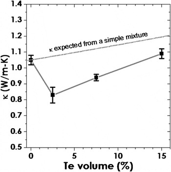
While we have confirmed a power factor enhancement in the Te-inclusion samples, ZT is the most important factor for practical applications. For estimating the ZT, thermal conductivities of the first sample set were measured at room temperature with a 2ω methodReference Kato and Hatta33 using a ULVAC-Riko TCN-2ω thermal conductivity measurement system. The measurement is based on the electric periodic heating and the thermoreflectance methods, measuring thermal conductivities in the direction normal (i.e., vertical) to the film surface.Reference Kato and Hatta33 The temperature increase on the sample surface can be analyzed on the basis of on-dimensional heat conduction model along the direction normal (i.e., vertical) to the film surface.Reference Kato and Hatta33 The typical error using this technique is probably larger than 10%. However, the comparison between the samples in this case should be valid. The measured thermal conductivities for the 0%, 2.5%, 7.5%, and 15% Te-added samples are shown in Fig. 6. The error bars refer a deviation from repeated measurements. Te-free sample exhibited κ of 1.05 W/(m K) at room temperature, and the Te-embedded samples showed κ values of 0.83–1.09 W/(m K). The thermal conductivity was reduced by embedding nanosized particle up to 7.5% addition. Because the increase of thermal conductivities was anticipated due to much higher thermal conductivity of ∼ 3 W/(m K) (at 300 K) in a simple mixture of the Bi0.5Sb1.5Te3 matrix and Te metal, it is clearer that the thermal conductivity was reduced in these nanoparticle-embedded samples. Thermal conductivity expected from the simple mixture was roughly estimated from a simple Maxwell’s equation,Reference Maxwell34 and indicated in a dotted line in Fig. 6 for reference. Thus, we could conclude that there is clear phonon scattering due to nanosized Te particles embedded in the matrix. The results support that the interfaces produced by the embedded nanosized Te particles enhanced phonon scattering, resulting in hindering the phonon transport through the matrix.Reference Kim, Zide, Gossard, Klenov, Stemmer, Shakouri and Majumdar35–Reference Zhang, Zhang, Jiang, Xiong, Chen, Zhang, Li and Xu37 This result is consistent with the prior theoretical result that the mid-to-long wave length phonons could be effectively scattered by nanoparticles of nanoinclusions.Reference Kim, Zide, Gossard, Klenov, Stemmer, Shakouri and Majumdar35 It seems that the effective scattering of phonons due to the Te nanoparticle addition may be saturated at around Te contents of 2.5% in this case.
Measured thermal conductivities of the sample set I. The error bars refer a deviation from repeated measurements.

It should be noted that the thermal conductivities of the samples were measured in the normal direction of the film, whereas their electrical properties were characterized in the in-plane direction. Therefore, we did not calculate the dimensionless figure of merit ZT in this work due to the different measurement direction. However, both the power factor increase and the thermal conductivity reduction should be valid in the both directions due to the relatively homogeneous dispersion of Te nanoparticles as seen in Figs. 2(b)–2(d). If the ratios of the thermal conductivity reduction and power factor increase are isotropic, ZT could be expected to be increased by a factor of ∼1.5 at the 7.5% Te addition. The advantages of Te nanoinclusions are experimentally realized by both electron- and phonon scattering.
IV. CONCLUSIONS
From the idea that high density Te nanoparticles would provide both interface barrier potentials, allowing S to be increased through a carrier energy filtering effect, and phonon scattering centers causing a reduction of κ, we have fabricated a series of Te nanoparticle-embedded Bi0.5Sb1.5Te3 films by using an alternating deposition technique of ultrathin Te and a Bi0.5Sb1.5Te3 layer. The microstructural observations confirmed that Bi0.5Sb1.5Te3 films with high-density Te nanoinclusions were successfully fabricated. We have confirmed a S enhancement experimentally in so-called Pisarenko plots, and the S enhancement was explained based on the carrier energy filtering effect. The energy relaxation calculation was made to confirm that the Te nanoinclusions result in a carrier energy filtering effect in Bi0.5Sb1.5Te3. As a result, the thermoelectric power factors were enhanced, which implies direct enhancement of ZT. In addition, the total thermal conductivity was reduced in the Te-embedded Bi0.5Sb1.5Te3, permitting further enhancement of ZT. In the present case, ∼2.5–7.5 vol% Te nanoinclusions of ∼10–20 nm induced both power factor increase and total thermal conductivity reduction in Bi0.5Sb1.5Te3. The Te nanoparticles offer an effective approach to increase the ZT in BiSbTe alloys by enhancing the power factor and lowering the total thermal conductivity simultaneously.
ACKNOWLEDGMENTS
This research was supported by WCU (World Class University) program through the National Research Foundation of Korea funded by the Ministry of Education, Science and Technology (R31-2008-10029) and by the Human Resources Development program of the Korea Institute of Energy Technology Evaluation and Planning (KETEP) grant funded by the Korea government Ministry of Knowledge Economy.