I. INTRODUCTION
With the large-scale commercial adoption of the long-term evolution (LTE) and IEEE 802.11y standards, there is a renewed drive to find compact, low-loss, and low-cost implementations of S- and C-band microwave filters on conventional soft substrates. Substrate integrated waveguide (SIW) [Reference Deslandes and Wu1] filters have the advantage of high resonator Q-factor whilst requiring only a conventional two-layer RF PCB process to manufacture. The technology does, however, occupy more board space than equivalent planar resonators [Reference Chen, Wu and Li2] or off-board manufactured filters such as low-temperature co-fired ceramics (LTCC) [Reference Schulte, Ziegler, Schoenlinner, Prechtel and Schumacher3]. Apart from using multiple metalized layer geometries [Reference Grigoropoulos, Sanz-Izquierdo and Young4] or alternative cavity geometries [Reference Zhang, Hong, Wu, Chan and Hao5], SIW resonators have been miniaturized successfully by loading of the SIW cavities to create evanescent mode cavity (EMC) resonators (the operating theory of which is described in [Reference Yao, Zaki, Atia and Hershtig6]). This loading has been accomplished with dielectric posts [Reference Wu, Zhou, Zhou and Yin7], defected ground structures [Reference Huang, Shao and Liu8], complementary split-ring resonators (CSRRs) [Reference Dong, Yang and Itoh9], and capacitive posts [Reference Martínez, Sirci, Taroncher and Boria10]. This capacitive loading may be increased to the point where the area of the capacitive plate, and not the surrounding fencing, defines the resonator, as was shown with the TEM-SIW cavity [Reference Zhang and Guan11]. Another way of decreasing the width of SIW resonators is using half-mode guide (HMSIW) [Reference Zhou, Wang, Xu, Shen and Zhan12] which, unlike folded SIW [Reference Grigoropoulos, Sanz-Izquierdo and Young4], does not require multiple metalized layers. HMSIW has been successfully combined with CSRR [Reference Senior, Cheng and Yoon13], external capacitive loading [Reference Senior, Cheng and Yoon14] (to create a second transmission band), and fractal pattern miniaturization [Reference Sekar and Entesari15], but not with internal capacitively loaded resonators.
This paper presents a novel combination of the miniaturization properties of both HMSIW and capacitively loaded EMC resonators (similar to TEM-SIW resonators). The filter size is reduced further by removing the via fences still used in [Reference Martínez, Sirci, Taroncher and Boria10, Reference Zhang and Guan11] that demarcate separate cavities, relying solely on the capacitive load plate to define the resonator area.
II. GEOMETRY
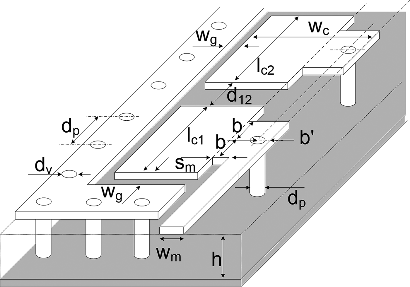
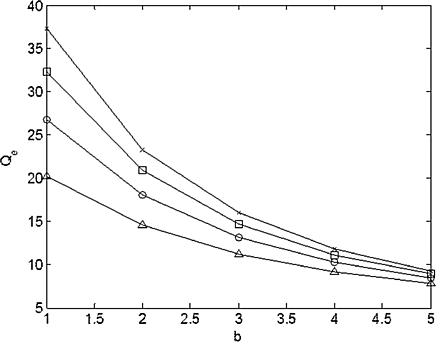
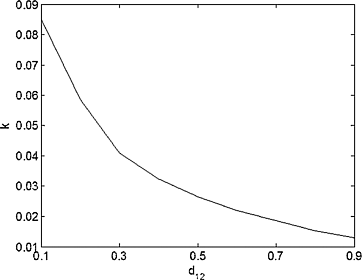
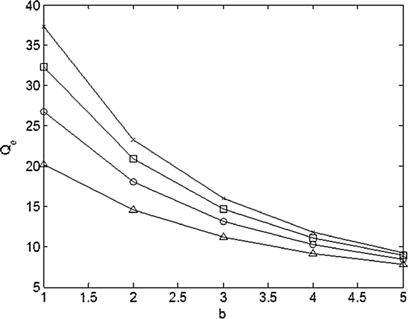
The structure of the capacitively loaded HMSIW is shown in Fig. 1. The first resonator is formed in a substrate of height h by a capacitive plate of width w c and length l c1, and is connected to ground by a post of diameter d p. The plate is separated from the edge of the SIW cavity (defined by a via fence of diameter d v and pitch d p) by a gap w g. The resonator is tapped-fed externally by a 50 Ω microstrip line of width w m, with the feed defined by a slot of width s m terminating a distance b from the post. The capacitive plate is connected to the center post by a septum of width 2b, with the post a distance b' from the edge of the metallization. The second resonator is formed by a plate of length l c2 and width w c, which couples to the first across the gap d 12. It is important to note the absence of via fencing between the resonators, further reducing the length of the final filter. Major changes to the external Q-factor of the resonator is achieved by varying the septum width 2b (Fig. 2), while minor alterations may be accomplished by varying the slot width s m. Coupling k between resonators is electric, with the distance separating them (d mn) controlling capacitive coupling. Coupling values of k = 0.01 → 0.09 are possible (Fig. 3).
Two cascaded resonators, with microstrip coupling to the first.

External Q-factor variation versus b. −Δ− : s m = 0.5; −○− : s m = 1; −□−: s m = 1.5; −X−: s m = 2.
Coupling k versus d mn.
III. SYNTHESIS AND SIMULATION
A third-order filter is synthesized with a passband to cover LTE channel 43 from 3.6 to 3.8 GHz, with −15 dB pass-band input reflection. This filter requires external resonator loading of Q e = 20.7 and internal coupling of k 12 = k 23 = 0.0476. Both parameters are related to geometric dimensions through the use of full-wave eigenmode solvers provided in CST Microwave Studio. The external Q-factor is determined by varying s m and b (with variation in l c1 to ensure resonance at f 0 = 3.7 GHz), and calculating the external Q-factor at the port of excitation. The even-mode and odd-mode eigenmode resonances f e and f o are used to calculate k in a simulation, with d 12varied to achieve the required value. After assembly and simulation of a full finite element method (FEM) model in CST, the filter is tuned to final dimensions in mm, as referenced to Fig. 1, of w m = 1.67, w g = 0.50, w s = 1.00, w c = 7.00, b = 0.53, b' = 0.84, d v = 0.50, d p = 1.00, d 12 = d 23 = 0.32, l c1 = l c3 = 7.40, l c2 = 6.90, and s m = 0.75.
IV. MANUFACTURING AND MEASURED RESULTS
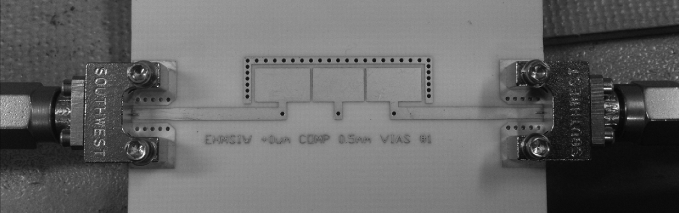
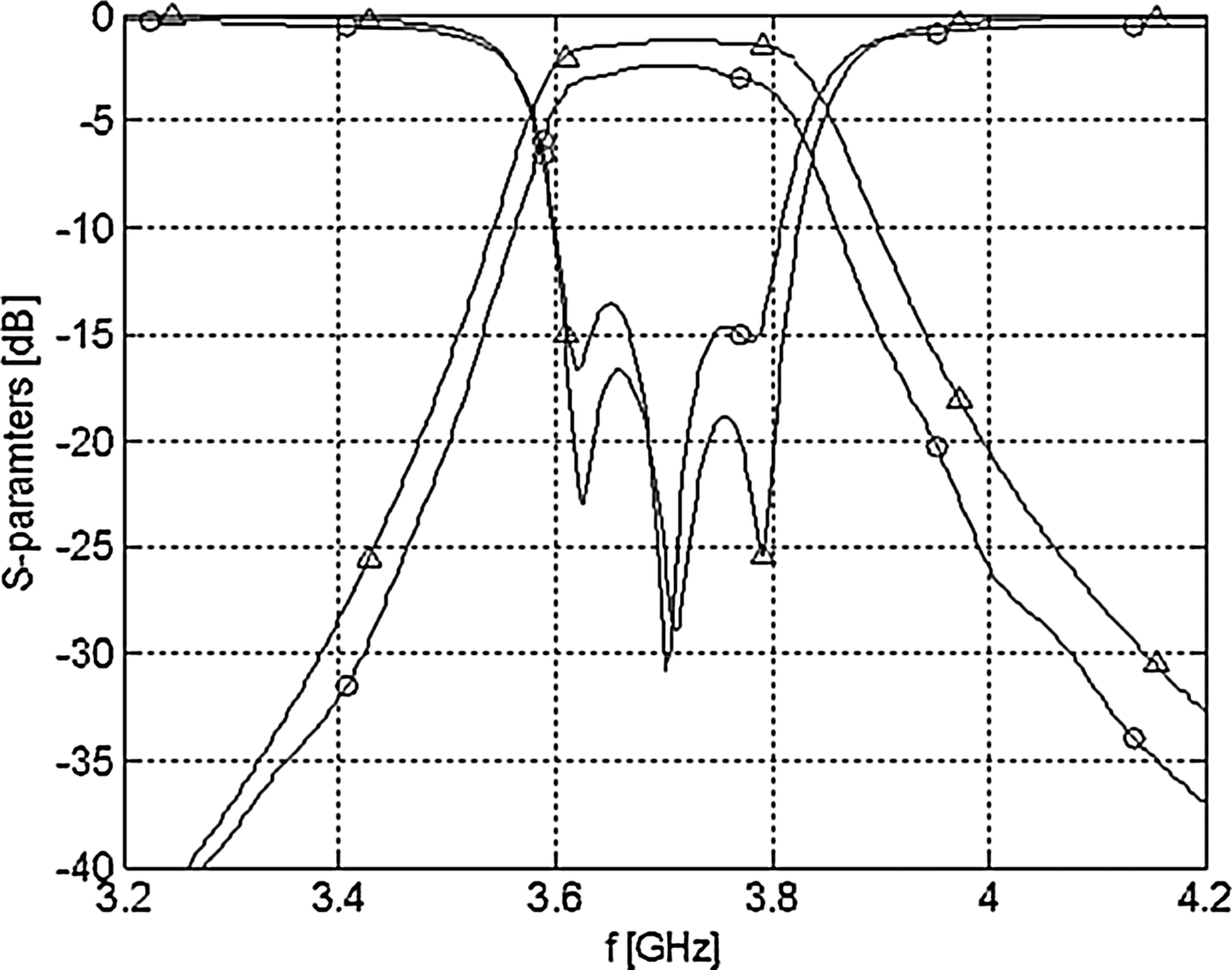
The prototypes were manufactured on Rogers RO4003C of thickness 0.813 mm, using 1 oz. copper deposition, as shown in Fig. 4. The artwork exported from CST Microwave Studio was compensated for +9 µm over-etch on the copper tracks and +50 µm over-drill on the vias. These changes resulted in a manufactured filter with negligible center frequency offset from the simulated result (Fig. 5). The additional 1.1 dB insertion loss is attributed to lower than expected resonator Q-factor, an assumption substantiated by the rounded filter response at the upper and lower cut-off frequencies. The lower Q-factor is attributed to the electroless nickel immersion gold surface finish, which is known to cause larger than anticipated insertion loss in planar filters [Reference Stander, Diniz and Sinha16].
Photographed filter under test.
Simulated −Δ− and measured −○− filter responses.
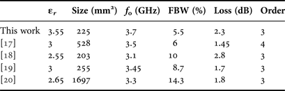
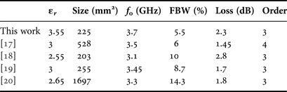
This work is compared in Table 1 to the state-of-the-art in compact LTE filters on conventional RF substrates. For comparable filter order, fractional bandwidth (FBW), and frequency, the filter occupies less board space than state-of-the-art solutions at the expense of higher insertion loss.
Comparison of this work to the state-of-the-art in uni-planar LTE filters.
V. CONCLUSION
A miniaturized SIW filter, suitable for LTE and IEEE 802.11y applications, has been presented. The filter measures 225 mm2 and features 2.3 dB insertion loss across a 5.5% FBW for upper LTE channel frequencies. Good first-iteration agreement between simulated and measured results is obtained, both in center frequency and bandwidth.
ACKNOWLEDGEMENTS
The authors wish to thank CST Computer Simulation Technology AG for the use of CST Microwave Studio under the educational license, National Instruments Inc. for the use of AWR Microwave Office, and Denel Dynamics (a Division of Denel (Pty) Ltd.) for materials and manufacturing. This work was supported by the Eskom Tertiary Education Support Programme (TESP).
 Tinus Stander, SMIEEE, obtained his B.Eng. and Ph.D. (Electronic Engineering) degrees from Stellenbosch University, South Africa. After practicing as RF and Microwave Engineer at Denel Dynamics, a division of Denel SOC Ltd., he joined the University of Pretoria (UP), where he currently serves as Senior Lecturer with the Carl and Emily Fuchs Institute for Microelectronics, Department of Electrical, Electronic and Computer Engineering. Dr. Stander currently leads the University of Pretoria's mm-Wave research focus, and also acts as consultant to various industries through Business Enterprises at UP (Pty) Ltd. He volunteers as Secretary for the joint IEEE chapter: Antennas and Propagation, Microwave Theory and Techniques (MTT) & Electromagnetic Compatibility Society, as well as faculty advisor to the University of Pretoria MTT Student Chapter, IEEE South Africa Section. He was recently awarded an Erasmus Mundus EUROSA III scholarship.
 Saurabh Sinha, SMIEEE, FSAIEE, obtained his B. Eng., M. Eng., and Ph.D. (Electronic Engineering) degrees from the University of Pretoria (UP), South Africa. After more than a decade of service to the UP, Professor Sinha now serves as Executive Dean: Faculty of Engineering and the Built Environment, University of Johannesburg, South Africa. He has authored or co-authored over 60 publications in peer-reviewed journals and at international conferences. Saurabh was elected to serve the IEEE as the 2014 Vice-President: Educational Activities. Saurabh is the managing editor of the South African Institute of Electrical Engineers (SAIEE) Africa Research Journal. Over and above his scholarly contributions, Saurabh, a registered professional engineer, also served as an industrial consultant for Business Enterprises at UP (Pty) Ltd. In 2007 Saurabh received the SAIEE Engineer of the Year award, 2010 University of Pretoria Laureate award, and 2013 T.W. Kambule NRF/NSTF Award.