Introduction
Historically, the term microelectromechanical systems (MEMS) has been used to identify sensors and actuators that are microfabricated using manufacturing processes such as those employed for the making of integrated circuits (ICs). In most cases, MEMS devices are fabricated on or from silicon wafers and made out of the same type of materials that are conventionally used for the synthesis of complementary metal oxide semiconductor (CMOS) technologies, such as polysilicon, silicon dioxide, silicon nitride, and aluminum. In the early stages of MEMS development (starting around 1960), piezoelectric materials were rarely used and mostly restricted to ZnO, as it was hard to access deposition techniques that would guarantee repeatable results. Furthermore, the most common piezoelectric used for the making of macroscale transducers was lead zirconate titanate (PZT), a material that was more difficult to process and integrate as a thin film on silicon (although, as shown in the Pulskamp et al. article in this issue, many of these issues are now resolved), exhibits quality factors that are too low for some RF applications, and especially was of concern to IC fabrication facilities because of contamination risks in CMOS lines. Thin-film zinc oxide (ZnO) also suffered from similar issues, and its reactivity with other IC materials made it hard to integrate with standard CMOS processes.
With the introduction of aluminum nitride (AlN) and especially the commercial success of the thin-film bulk acoustic resonator (TFBAR or FBAR),Reference Ruby1 interest in piezoelectrics for MEMS blossomed. It is fair to state that industry drives for more compact and cheaper radio frequency (RF) duplexers (for details, see next section), and the consequent investments in the development of repeatable physical vapor deposition (PVD) techniques for the growth of AlN films on silicon have spurred a great deal of activities in the field of piezoelectric and especially AlN MEMS. Practically, most conventional MEMS devices that used to be made out of silicon have recently been reproduced (in most cases with enhanced performance) by using AlN thin-film piezoelectric technology. For example, resonators,Reference Piazza, Stephanou and Pisano2–Reference Bjurstrom, Katardjiev and Yantchev5 filters,Reference Chengjie, Sinha and Piazza6–Reference Ruby, Bradley, Larson, Oshmyansky and Figueredo8 switches,Reference Mahameed, Sinha, Pisani and Piazza9–Reference Sinha, Jones, Zhijun and Piazza11 energy harvesters,Reference Elfrink, Kamel, Goedbloed, Matova, Hohlfeld, van Andel and van Schaijk12–Reference Ting-Ta, Hirasawa, Wright, Pisano and Liwei14 ultrasonic transducers,Reference Guedes, Shelton, Przybyla, Izyumin, Boser and Horsley15, Reference Shelton, Mei-Lin, Hyunkyu, Horsley, Boser, Izyumin, Przybyla, Frey, Judy, Nunan, Sammoura and Ken16 microphones,Reference Littrell and Grosh17, Reference Williams, Griffin, Reagan, Underbrink and Sheplak18 strain sensors,Reference Goericke, Chan, Vigevani, Izyumin, Boser and Pisano19 chemical sensors,Reference Zuniga, Rinaldi, Khamis, Johnson and Piazza20 and accelerometersReference Olsson, Wojciechowski, Baker, Tuck and Fleming21 have been demonstrated using AlN thin films.
This article reviews MEMS development using AlN, with a particular focus on RF applications and the development of micromechanical resonators for filters and oscillators. The article reports on FBARs for duplexers, explaining the technological need that drove the development of AlN thin-film devices and how FBAR has addressed these industry requirements. The focus is then shifted to another class of resonators, known as laterally vibrating, contour-mode (CMR) or lamb-wave resonators. These devices, having their center frequency set by lithographic techniques rather than film thickness, were introduced with the intent of producing multiple frequency filters and oscillators on the same silicon wafer, a feature that is difficult to attain with FBARs. Although the limited electromechanical coupling of the CMR does not make it a competitive solution for most commercial filtering standards, the technology is reviewed as an interesting development of AlN MEMS for oscillators and an example of the direct integration of AlN with CMOS. In fact, a unique aspect that makes AlN MEMS particularly attractive over other piezoelectrics is its ability to be deposited directly on top of CMOS. This feature would eventually enable a vision in which MEMS and circuits co-exist on the same chip, and silicon is used pervasively to interface with the analog world, perform sensing and actuation, signal processing, and computing. Finally, an outlook into material developments related to the deposition of Sc-doped AlN and nanoscale AlN films (<200 nm) is provided to show how the range of applicability of this thin-film technology will continue to grow. Sc-doped AlN enables piezoelectric films with higher intrinsic electromechanical coupling, for example extending the bandwidth of duplexers. Nanoscale AlN films permit the development of higher frequency resonators and will ultimately make on-chip and compact filtering attractive for more wireless standards.
Thin-film bulk acoustic resonators
Unlike most components in the radios for mobile phones (and there are many radios in today’s mobile phone), the duplexer (which sits right behind the antenna and in front of the power amplifier of the transmit chain and the low noise amplifier of the receive chain) allows for simultaneous transmission and reception of radio signals. It does this by separating transmit from receive in the frequency domain. The performance of the duplexer directly impacts the number of dropped calls and the talk time of the phone and will determine if a phone is in compliance with the US Federal Communications Commission (FCC) specifications (or the FCC equivalent in other countries). The most fundamental considerations are that the duplexer must have sufficient isolation and rejection to not interfere with other phones and to have low receive (Rx) and transmit (Tx) insertion loss over the full mandated bandwidth—typically 3%. In 2001, FBAR duplexers forever changed the shape of phones by eliminating the large ceramic block duplexers needed to perform the function of separating the transmit signal from the receive signal.
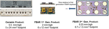
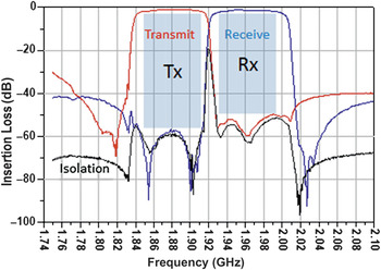
Each filter (Tx and Rx) is composed of resonators. To keep the filter response flat or nearly flat over the ∼3% bandwidth, the resonators need to have a coupling coefficient, k t2, of ∼6%. The coupling coefficient can be thought of as the efficiency of converting electrical fields to acoustical fields. Only a small group of piezoelectric resonators have the demonstrated coupling. Quartz, a weakly piezoelectric material, has a coupling coefficient of only ∼0.3% and cannot be used. Traditionally, materials such as lithium tantalate or lithium niobate, with their excellent coupling coefficients, were used as piezoelectric substrates, and metal fingers (called interdigitated transducers) were patterned to generate surface acoustic waves. It is found that the quality factor, or Q, of such surface acoustic wave (SAW) devices, while good (Qs ranging from 500 to a 1000), are not very high, thus limiting their performance compared to FBAR. The use of inductors and capacitors to form resonators can have the desired coupling, but the Qs of typical inductors vary from 10 to 20. Poor Q causes the roll-off (steepness of the “skirts” measured at the edge of the filter band pass region—in frequency space) to be extremely poor as well as “soft shoulders” at the band edges, thus violating the required isolation and insertion loss. In contrast, piezoelectric resonators have Qs in excess of 1000 (FBAR resonators now achieve a greater than 4000Reference Ruby1). Figure 1Reference Ruby, Bradley, Oshmyansky, Chien and Larson3 (middle image) shows the earliest FBAR duplexer (measuring 6 × 12 × 2 mm2). Also shown (right image) is the world’s smallest duplexer that has far better performance but has dimensions of only 0.7 × 1.5 × 0.23 mm2. Figure 2 shows the duplexer electrical response versus frequency. Here, the separation between transmission frequencies and receive frequencies are seen. The closer the insertion loss in the pass band gets to zero loss, the lower the power needed by the power amplifier and hence, longer battery life.
Duplexers from 1999 (ceramic duplexer) to the first-generation Avago Duplexer (2001) to the latest generation duplexer integrated into a single chip (DISC)—an all-silicon chip-scale packaged part. Note: FBAR, thin-film bulk acoustic resonator; Tx, transmit; Rx, receive; ANT, antenna.

Filter response of an Avago Personal Communications Service Duplexer. The transmit filter (red) allows frequencies from 1850 to 1910 MHz, and the receive filter (blue) allows frequencies from 1930 to 1990 MHz. The black curve is the isolation between the transmit (Tx) and the receive (Rx) band.

It should be pointed out that for filters used in the mobile space, the critical figure of merit (FOM) is the k t2-Q product. In the case of oscillators, Q is a very important parameter but is often mislabeled as the FOM. A better FOM would be the frequency-Q, or f-Q product. The reason for this is that a resonator with a 2x higher frequency but half the Q can have equal phase noise in an oscillator by simply dividing the output frequency using a divider. It should also be noted that one can sometimes trade k t2 for Q, but not Q for k t2. Reducing k t2 is not an option for mobile applications, since k t2 must always be roughly 2x the government assigned bandwidth. The higher the k t2-Q product, the better the insertion loss and isolation. Where the Tx and Rx bands are squeezed too close (to maximize spectral efficiency and/or because pre-existing frequency bands preclude adequate spacing and guard bands around the mobile frequency bands), very high k t2-Q products are a must. One of the reasons an FBAR has much higher Qs than SAWs (∼4x higher) is that the membrane containing the AlN and electrodes is isolated in air—being only connected at the edges—and little or no energy is therefore lost from the bulk of the membrane into air. One large source of acoustic energy loss is out through these “anchor points.” However, good design can minimize this source of loss and thus better trap the acoustic energy inside the membrane.
The first FBAR duplexers focused on the CDMA (code division multiple access) band at ∼1.9 GHz (often referred to as the Personal Communications Service band in the United States). The Rx and Tx bands were 60 MHz (or ∼3%) wide and separated by a narrow 1% guard band (i.e., the separation between the Tx pass band and the Rx pass band). The earliest FBAR duplexers had a k t2-Q product of ∼60. This was barely sufficient to meet CDMA requirements. Today, FBARs routinely show k t2-Q products of 250 to 300. Not surprising, as CDMA 2G was replaced by 3G and now 4G networks, the requirements on the filters have increased. Fast data rates demand receive sensitivities on the order of –111 dBm (in 2001, the spec was –103 dBm). Simultaneous voice and data require extreme linearity as well as excellent insertion loss. Linearity is dependent on isolation and increasingly the ability to suppress intrinsic non-linearities of the AlN material itself.
What makes the FBAR a huge success story (in 2002 about 1 million FBAR duplexers were sold; today, well over a billion or more are sold a year) is the confluence of many factors, but, clearly in the center of the success is the AlN film. Essential to the piezoelectric properties is the need to grow textured AlN (with c-axis perpendicular to the substrate) via a physical sputtering process (please see last section for further details). The intrinsic coupling coefficient of AlN is conveniently twice that of a typical FCC mandated transmit band; the dielectric constant was only 10. In contrast, the dielectric constant of lithium niobate and lithium tantalate ranges from 30 to 40. The velocity of sound is very high (10,600 m/sec). This means that wavelengths are relatively large, and critical dimensions that affect frequency accuracy are somewhat relaxed. The material is extremely stable and very hard (hardness being a good indicator of what the ultimate Q can be).
Work started in AlN in the early 1980s.Reference Grudkowski, Black, Reeder, Cullen and Wagner22, Reference Nakamura, Sasaki and Shimizu23 Unlike SAW materials, AlN can be used in a bulk wave thickness extensional mode (such as an accordion). It must be pointed out that there are many modes in a piezoelectric plate. The most understandable mode (and the mode with the largest effective coupling coefficient) is the extensional thickness mode. In a plate consisting of a film of AlN sandwiched between two electrodes, the electric field couples nearly 100% with acoustic stress fields. This overlap between electric and stress fields guarantees that the effective coupling coefficient is also about 6%.
Another fortuitous advantage of AlN is that it is a material that can be easily integrated into existing IC (integrated circuit) facilities (in contrast, ZnO, another piezoelectric material that can be grown as films with a similar or higher coupling coefficient—but much higher dielectric constant and slower velocity of sound—is poisonous to silicon processing). Furthermore, the making of the device (including the chip-scale, all-silicon package) utilizes nearly all the existing tools found in IC facilities. By adding a few MEMs tools (like a wafer bonder) to the arsenal of IC fabrication tools, one can make a complete all-silicon, hermetically packaged chip-scale filter/duplexer that meets yet one more criteria for cell phones—size.
Laterally vibrating contour-mode AlN resonators
In the near future, a more efficient utilization of the electromagnetic spectrum will require resorting to reconfigurable RF front ends capable of switching between different bands and rapidly adapting to incoming signals and interferers. Cognitive radios capable of sensing the available RF spectrum and selecting a desired frequency band for receiving and transmitting signals have been envisioned. Multifrequency filters and synthesizers are some of the core components that are required to implement such systems. CMOS-integrable MEMS resonators that operate over multiple frequencies on the same silicon chip are an attractive option for the development of these components.Reference Piazza24 The ability to span multiple arbitrary frequencies on the same silicon die offers a compact and possibly low-cost implementation of the envisioned reconfigurable system without the need for additional packaging or external bonding.
To this purpose, a laterally vibrating MEMS resonator made out of AlN thin film has been developed.Reference Piazza, Stephanou and Pisano2, Reference Chengjie, Sinha and Piazza6, Reference Rinaldi, Zuniga, Chengjie and Piazza7, Reference Piazza, Stephanou and Pisano25 This device (Figure 3) is formed by a suspended AlN film sandwiched between patterned metal electrodes (interdigitated transducers as in SAW devices) and is excited to vibrate in a length or width-extensional mode (also labeled as a Lamb mode if treated as an acoustic plate) through the equivalent d 31 piezoelectric coefficient.Reference Cady26 It is known as a CMR or Lamb-wave resonator. Different from the FBAR in which the center frequency is set by the film thickness, the CMR frequency is determined by its lateral, in-plane dimensions, more specifically the electrode pitch. In this case, lithography instead of film deposition is used to control the device center frequency, and therefore multiple frequency devices can co-exist on the same silicon wafer. In line with CMOS evolution, this will also yield a progressively scalable technology. A variation of a pure AlN implementation has also been pursued in which the same patterned AlN film is used to transduce a generally larger volume of siliconReference Harrington and Abdolvand4, Reference Lavasani, Abdolvand and Ayazi27—a solution that intrinsically trades k t2 for Q.
(a) Schematic representation of the basic building block of an AlN contour-mode resonator (CMR) and (b) its arrangement into multiple units forming a plate with interdigitated transducers (IDT). The electrodes are shown in red and blue to distinguish their polarity. The AlN film is shown in green. The superimposed finite element plot is shown to intuitively describe the mode of vibration (displacement) of the device. (c) Scanning electron micrograph of a 4.5 GHz AlN CMR is shown highlighting the input (red) and output (blue) electrodes. The equation for the device resonance frequency, f 0, is also shown with the proportionality factors for the motional resistance, R m, and device static capacitance, C 0. Note: T, thickness; W, width; L, length; Y eq, equivalent Young’s modulus; ρ eq, equivalent mass density; n, number of IDT.

AlN CMR devices have been demonstrated to span a broad range of frequencies (10s of MHz to 10 GHz) with low motional resistance (<50 Ω) and high Q in air (as high as 4,000 at 1 GHz). Because the CMR resorts to lateral vibrations in AlN films, it results in a k t2 of around 2%, about 3x lower than that for the FBAR. For this reason, this technology has been of most interest for the demonstration of narrow band filtersReference Chengjie, Sinha and Piazza6, Reference Rinaldi, Zuniga, Chengjie and Piazza7 (such as intermediate frequency filters) and oscillatorsReference Chengjie, Sinha, Van der Spiegel and Piazza28–Reference Rinaldi, Chengjie, Van der Spiegel and Piazza30 rather than commercial wideband applications.
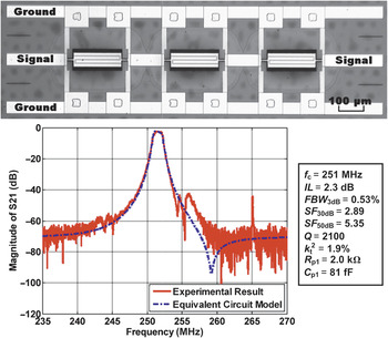
An example of a low loss and compact filterReference Chengjie, Sinha and Piazza6 around 251 MHz is shown in Figure 4. The filter was formed by simply cascading identical AlN resonators. The high Q and k t2enable the demonstration of a filtering solution capable of <3 dB of loss in approximately 1/20th of the volume of a SAW counterpart. The high linearity of the material system also ensures attaining a high third order intermodulation distortion product (IIP3 > 40 dBm) and good power handling.
A scanning electron micrograph and transmission response of a 251 MHz 3rd order filter made out of AlN contour-mode resonators. Low insertion loss (IL) in a small form factor has been attained. Note: f c, filter center frequency; FBW 3dB, filter fractional bandwidth; SF 30dB, 30 dB shape factor; SF 50dB, 50 dB shape factor; Q, quality factor; k t2, electromechanical coupling coefficient; R p1, parasitic resistance; C p1, parasitic capacitance.

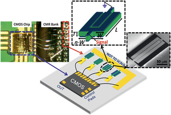
An example of a reconfigurable oscillatorReference Chengjie, Sinha, Van der Spiegel and Piazza28, Reference Rinaldi, Chengjie, Van der Spiegel and Piazza30 that employs high Q AlN MEMS resonators at four selected frequencies of operation is shown in Figure 5. This system is formed by multifrequency (268, 483, 690, and 785 MHz) switchable AlN CMRs that are simultaneously connected to a single CMOS oscillator circuit. The resonators are selected by means of properly designed CMOS switches, and the oscillator can be configured to selectively operate in four different states with distinct oscillation frequencies by an on-chip decoder. Jitter (a measurement of the deviation from periodicity of an electronic signal) values as low as 114 fs-rms (root-mean square) (integrated 12 kHz—20 MHz) and switching times as fast as 20 μs were measured. This first prototype exhibits jitter values comparable to commercially available voltage controlled SAW oscillators (VCSOs), but it is 30x smaller than dual-frequency counterparts and has the advantage of generating multiple stable frequencies by employing high-quality factor mechanical elements. This is one of the first implementations of compact and multifrequency banks of high Q mechanical elements, using thin-film AlN, which could be used for the fabrication of next-generation reconfigurable local oscillators for RF transceivers.
Schematic view and micrograph of the reconfigurable complementary metal oxide semiconductor (CMOS) oscillator prototype based on four different-frequency AlN contour-mode microelectromechanical system resonators. The insets show a schematic representation and a scanning electron microscopy image of one of the contour-mode resonators (CMR). Note: T, thickness; L, length; W, width; n, number of interdigitated transducers.

AlN resonators on CMOS circuits
One advantage of AlN as a microsystems material is its ability to realize thin films with excellent piezoelectric (high coupling coefficient) and acoustic (low damping, high sound velocity) properties at deposition temperatures compatible with integration over CMOS transistors (<400°C). Post-CMOS integrationReference Fedder, Howe, Tsu-Jae King and Quevy31 enables compatibility with state-of-the-art foundry-based fabrication technologies, including those with RF passives, such as inductors, silicon germanium bipolar transistors for low noise RF amplifiers, and fine line CMOS transistors at the forefront of digital signal processing. While AlN microsystems can be integrated with CMOS transistors to reduce size, cost, and component count in RF and sensor systems, there are additional performance benefits provided through integration. The coupling coefficient of a piezoelectric resonator is defined by the ratio of the motional capacitance to the electrical capacitance. Thus, any additional electrical capacitance contributed by bond pads or interconnect traces used to route to a piezoelectric resonator decreases the effective coupling coefficient. Switched filter arrays for RF band or channel selection, such as those reported in Reference 32, can yield higher numbers of bands/channels or lower insertion loss by eliminating parasitic interconnect capacitance via integration. Similarly, the Pierce oscillators reported in References 33 and 34 require lower transistor current when interconnect and bond pad parasitic capacitances are reduced. Piezoelectric resonators connected in a Pierce oscillator circuit are commonly used to provide the highly stable oscillators required in modern radio frequency communications systems such as cell phones and radars.
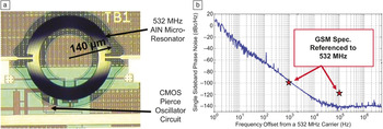
Numerous examples of both FBARReference Carpentier, Cathelin, Tilhac, Garcia, Persechini, Conti, Ancey, Bouche, Caruyer, Belot, Arnaud, Billard, Parat, David, Vincent, Dubois and Enz36–Reference Sung, Fang, Chang, Chin and Chen39 and contour mode AlN microresonator integrationReference Crespin, Olsson, Wojciechowski, Branch, Clews, Hurley and Gutierrez32, Reference Wojciechowski, Olsson, Tuck, Roherty-Osmun and Hill33 with CMOS transistors have been reported in the literature with little to no degradation in piezoelectric or acoustic properties. One such example is the Pierce oscillator formed from an AlN contour mode ring resonator integrated directly over CMOS circuitry reported in Reference 35 and shown in Figure 6a. Figure 6b shows the measured phase noise (a measurement of the oscillator short term frequency stability) of the single chip oscillator and specifications, converted to 532 MHz, frequency reference for the global system for mobile communications (GSM), a common standard for mobile phones. The AlN/CMOS oscillator demonstrates communications grade phase noise performance, and when combined with separately developed thermal stabilizationReference Kim, Olsson and Wojciechowski40 and wafer level packagingReference Chanchani, Nordquist, Olsson, Peterson, Shul, Ahlers, Plut and Patrizi41 techniques, it is a viable technology for integration with RF electronics in next-generation military radios and wireless handsets.
(a) Image of a 532 MHz AlN contour-mode ring resonator integrated directly over a complementary metal oxide semiconductor (CMOS) Pierce oscillator circuit.Reference Olsson, Wojciechowski, Tuck, Stevens and Nordquist35 (b) The measured phase noise of the oscillator and a comparison to the phase noise specifications for a global system for mobile communications (GSM) frequency reference. The single chip AlN microelectromechanical system oscillator achieves communications grade phase noise performance.

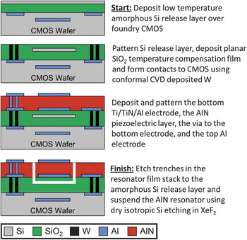
The process flow used to fabricate the AlN microresonator over CMOS is shown in Figure 7.Reference Chengjie, Sinha and Piazza6 The process begins with planarized foundry CMOS wafers followed by the deposition and patterning of a 600-nm-thick low temperature (400°C) amorphous Si (a-Si) release layer. Next, a temperature compensation oxide is deposited, and vias are etched on the top CMOS metal layer. The vias, which are several microns deep, are filled by conformal chemical vapor deposition (CVD) of W, which is subsequently polished to remain only in the vias. The remaining process proceeds like a non-CMOS integrated AlN microresonator fabrication flow, including the deposition and patterning of a resonator bottom Al electrode, piezoelectric AlN layer, and resonator top Al electrode. Finally, the resonator film stack is etched to the a-Si layer, and the resonator is suspended from the substrate using an isotropic Si etch in gaseous XeF2. The key technologies for achieving post-CMOS integration are the low temperature release layer and AlN deposition, the conformal W deposition allowing for deep, high aspect ratio vias to the underlying CMOS, and protecting the Si-CMOS from the release chemistry.
Fabrication process used for post-CMOS integration of the microresonator oscillator shown in Figure 6.

The ability to achieve many resonant frequencies on a single substrate and to monolithically integrate with electronic configuration circuitry makes AlN microresonators a critical technology for realizing next-generation radios that can sense and adapt to the RF environment. In the future, single chip radios with banks of microresonator filters and oscillators covering multiple bands will enable more efficient and reliable utilization of the RF spectrum. Resonator arrays that reconfigure not just filter center frequency but also filter 3 dB bandwidth, number of poles, and the location of notches or nulls in the transmission response to reject strong interfering signals will be developed. With increases in the resonator coupling coefficient, such as those described in the following section, AlN microresonators on CMOS may also replace many of the discrete filters in modern cellular handsets with a single reconfigurable filter die.
Doped AlN films
The piezoelectric coupling coefficient of a thickness mode resonator—based on a longitudinal wave perpendicular to the film plane, thus along the 3-direction for a (001)-oriented film—is limited by the material coupling coefficient  $k_{\rm{t}}^{\rm{2}} = e_{33}^2 /(c_{33}^{\rm{D}} {\rm{\varepsilon }}_{{\rm{33}}}^{\rm{S}})$, where
 $e_{33}^{}$ is the piezoelectric stress coefficient,
 $c_{33}^{\rm{D}}$ is the relevant stiffness constant, and
 ${\rm{\varepsilon }}_{33}^{\rm{S}}$ is the relevant dielectric constant. In today’s FBARs, the piezoelectric plate is formed by a c-axis oriented AlN thin film. According to standard literature dataReference Tsubouchi and Mikoshiba42 of epitaxial AlN thin films,
 $k_{\rm{t}}^{\rm{2}}$ is 6.8%. For real resonators, the effective coupling coefficient
 $k_{{\rm{eff}}}^2 ,$, as derived directly from resonator characteristics, reached slightly larger values of 7%,Reference Lakin, Belsick, McDonald and McCarron43 indicating that optimized AlN films reach somewhat higher piezoelectric coefficients than values usually used as standard data.
This is in fact compatible with low frequency measurements of the clamped coefficient  $d_{33,{\rm{f}}} = e_{33} /c_{33}^{\rm{E}}$ (
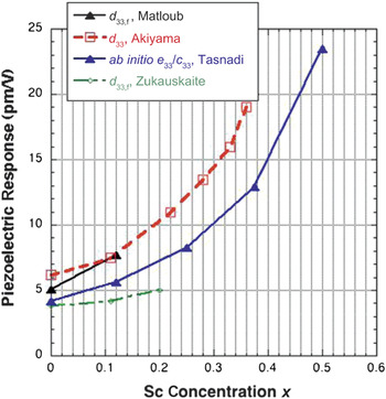
 $c_{{\rm{33}}}^{\rm{E}}$ is the stiffness at constant electric field E), which reaches 5.1 pm/V instead of 3.9 pm/V.Reference Martin, Muralt, Dubois and Pezous44 The effective coupling coefficient governs the filter bandwidth. As previously stated, the values achieved in pure AlN are high enough to fulfill today’s filter specifications for the various mobile phone bands around 2 GHz. However, there are other filter types and applications that would require larger coupling factors in order to achieve larger bandwidths.
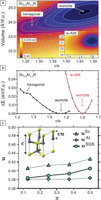
Recently, it was shown that Al substitution by Sc allows for an increase of the piezoelectric response.Reference Akiyama, Kamohara, Kano, Teshigahara and Kawahara45, Reference Akiyama, Kamohara, Kano, Teshigahara, Takeuchi and Kawahara46 This was predicted earlier for the (Ga,Sc)N system based on first-principle calculations,Reference Alsaad and Ahmad47 with the idea that a solid solution system going from a piezoelectric wurtzite structure on the Ga rich side to a non-piezoelectric rock-salt structure on the Sc rich side would exhibit a region somewhere within the wurzite phase where piezoelectricity would peak, similar to a para-to-ferroelectric phase transition, occurring in this case, however, as a morphotropic phase transition. In reality, there is an intermediate non-piezoelectric hexagonal structure.Reference Takeuchi48 Recently, it was shown by density functional theory that substitution of Al by Sc leads indeed to a softening of the wurtzite phase, interpreted as a competition of Al3+ and Sc3+ ions about the coordination of nitrogen (Al3+ preferring 4-fold, and Sc3+ preferring 6-fold coordination) that results in a trend to weaken the wurtzite phase with increasing Sc content.Reference Tasnadi, Alling, Höglund, Wingqvist, Birch, Hultman and Abrikosov49 The intermediate hexagonal structure exhibits 5-fold coordination, lying in-between the 4-fold for wurtzite and the 6-fold of rock salt. With increasing Sc concentration in the wurtzite phase, the potential wells of the ions become shallower (see Figure 8), and thus the ionic displacements in an electric field become larger, leading to larger piezoelectric stresses as a function of electric field, for instance. It was found that the e 33increased, while the stiffness simultaneously decreased.Reference Tasnadi, Alling, Höglund, Wingqvist, Birch, Hultman and Abrikosov49
Structural modifications and phase stabilities in ScxA11–xN. Increased Sc concentration leads to a decreasing c/a ratio (increasing a). (a) The energy landscape for the combined hexagonal-wurtzite system and the wurtzite system (insert: axes are the same as main plot); (b) minimum energy (E) cross-sections; and (c) the change in the lattice parameter u of the wurtzite structure with concentration x (from Reference 49). Note: SQS, special quasi-random structure, which describes a method to handle alloy properties.

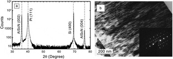
The typical AlN thin film yields good piezoelectric properties when grown on a smooth surface with a magnetron sputter source providing ion bombardment of the film with ions in a suitable energy and current range that ensures high ad-atom mobility on the surface of the growing film.Reference Artieda, Barbieri, Sandu and Muralt50–Reference Dubois and Muralt52 The suitable growth mode is within the T-zone of Thornton’s growth types.Reference Thornton and Hoffman53 The film grows in columns that are fiber like and exhibit a perfect (001) orientation. Hence, one of the first questions is whether this favorable growth mode is achieved as well with Sc additions, which might hamper adatom diffusion. In the first studies, the deposition processes for AlScN were based on RF co-sputtering from two magnetron sources with metallic Al and Sc targets, operated in a nitrogen–argon gas mixture.Reference Akiyama, Kamohara, Kano, Teshigahara and Kawahara45, Reference Akiyama, Kamohara, Kano, Teshigahara, Takeuchi and Kawahara46 Later, the same method was used supplying pulsed dc power to the two magnetrons instead of RF power,Reference Moreira, Bjurstrom, Katardjiev and Yantchev54 or simple dc power with small sources for research purposes.Reference Wingqvist, Bjurstrom, Liljeholm, Yantchev and Katardjiev55 For high throughput industrial processes, a single source using an alloy target is preferred. Such processes were successfully applied with either RFReference Akiyama, Tabaru, Nishikubo, Teshigahara and Kano56 or dc pulsed power supplies.Reference Matloub, Artieda, Milyutin and Muralt57 It was found in the latter case that the identical growth mode and microstructure type as with pure AlN can be reproduced, at least up to 12% of Sc. X-ray diffraction (XRD) and transmission electron microscopy (TEM) revealed pure c-axis orientation with a columnar microstructure (Figure 9), similar to that observed for undoped AlN thin films.Reference Muralt, Conde, Artieda, Martin and Cantoni58 The favorable microstructure is maintained as long as the Sc concentration is not too large and the growth temperature is not too high (i.e., not above about 400°C).
Microstructural analysis of an Al0.88Sc0.12N thin film grown on a Pt (111) bottom electrode at 300°C: (a) θ–2θ x-ray diffractogram; (b) transmission electron microscopy cross-section with the corresponding electron diffraction pattern in the inset (from Reference 57). Note: θ, angle between the incident x-ray beam and the incident plane.

In the first reports on (Al,Sc)N thin films, a very large increase in the piezoelectric d 33 activity was observed (Figure 10). However, the applied stress response technique was inadequate to precisely measure either the thin-film coefficient
 $$d_{33,{\rm{f}}} = {{e_{33} } \over {c_{33}^{\rm{E}} }}$$
Piezoelectric thickness mode coefficients in comparison.Reference Akiyama, Kamohara, Kano, Teshigahara and Kawahara45, Reference Matloub, Artieda, Milyutin and Muralt57 Note: d 33,f, derived from true thickness change measurements with double side interferometry; d 33, from Akiyama et al. by applying stress on film and substrate, ab initio values were calculated from first principles by Tasnadi et al.; e 33, piezoelectric stress coefficient; c 33 = c 33E, stiffness constant.Reference Zukauskaite, Wingqvist, Palisaitis, Jensen, Persson, Matloub, Muralt, Kim, Birch and Hultman59

or the standard d 33 coefficient, because the substrate was deformed as well. This results in a transverse contribution (from e 31) enhancing the response. Nevertheless, the increase was so strong that there was no doubt that d 33 or e 33 would increase as well. This was recently also confirmed by double-side interferometric measurements yielding d 33,f. The results are compared in Figure 10.
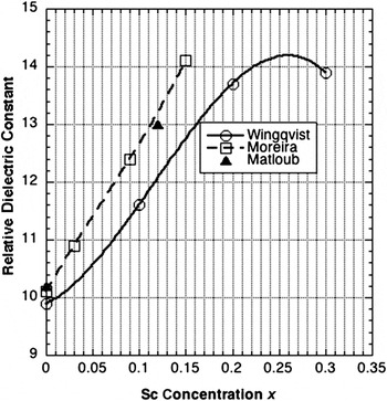
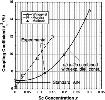
Softening of a material leads not only to a reduction in the stiffness, but also to an increase in the dielectric constant, as the displacement of the ions forced by the electric field is counterbalanced by the stiffness. No ab initio calculations are available for the dielectric response, but existing experimental data (Figure 11) confirm such an increase. Standard AlN thin films are expected to have a relative dielectric constant of 10.2.Reference Tsubouchi and Mikoshiba42 Sc increases the response to 13 for 12% Sc. Moreira et al.Reference Moreira, Bjurstrom, Katardjiev and Yantchev54 obtained a linear increase with Sc concentration, whereas Wingqvist et al.Reference Wingqvist, Tasnadi, Zukauskaite, Birch, Arwin and Hultman60 reported a saturation above 20% and a less steep increase. Matloub et al.Reference Matloub, Artieda, Milyutin and Muralt57 confirmed the finding of Moreira at x = 12%. Finally, the coupling coefficient is the most important aspect for the FBARs. A compilation of results is shown in Figure 12.Reference Moreira, Bjurstrom, Katardjiev and Yantchev54, Reference Matloub, Artieda, Milyutin and Muralt57, Reference Wingqvist, Tasnadi, Zukauskaite, Birch, Arwin and Hultman60 The experiments look more promising than predictions from ab initio calculations.
Dielectric response of AlScN thin films (composed from References 54, 57, and 60). A third power fit was applied to the curves.

Coupling coefficients of film bulk acoustic resonators (FBARs) with AlScN thin films obtained from experimentReference Moreira, Bjurstrom, Katardjiev and Yantchev54, Reference Matloub, Artieda, Milyutin and Muralt57 and ab initio with experimental values for the dielectric constant.Reference Wingqvist, Tasnadi, Zukauskaite, Birch, Arwin and Hultman60

In conclusion, (Al,Sc)N is a very promising material for larger bandwidths in filters for mobile communications. It is not clear yet to what extent the higher Sc concentrations are exploitable, as a limit might be imposed by the materials quality factor that will decrease with Sc doping.
Nanoscaled aluminum nitride films
In the near future, the burgeoning wireless market will demand further increasing operation frequencies from the current 1–5 GHz to K and Ka bands (up to 30 GHz range). As the resonance frequency of FBAR and bulk acoustic wave (BAW) resonators is inversely proportional to the thickness of the AlN layer, these super-high frequency devices will require AlN thin films to be scaled from a 500–2000 nm thickness to below 200 nm.Reference Ueda, Hara, Taniguchi, Yokoyama, Nishlhara, Hashimoto and Satoh61, Reference Iborra, Clement, Capilla, Olivares and Felmetsger62 Additionally, thinner films, 25 nm or below with precisely controllable in-plane stress as well as stress gradient through the film thickness, are required for a new class of vertically deflecting piezoelectric nanoelectromechanical actuators with an architecture involving thin AlN cantilever beams for low-power logic applications.Reference Sinha, Wabiszewski, Mahameed, Felmetsger, Tanner, Carpick and Piazza10
Today, reactive magnetron sputtering is the preferred method for growth of AlN films with a high degree of c-axis texture. The quality of the crystal orientation is usually characterized by the full width at half maximum (FWHM) of the x-ray rocking curve around the diffraction peak of AlN (0002). Better oriented films possess lower FWHM values. Aside from deposition conditions and substrate properties, FWHM is sensitive to film thickness: it reduces with increasing film thickness as a more thorough columnar texture develops. Widening of the rocking curve in thinner films is explained by a relatively high density of threading dislocations generated at the film-substrate interface to release stresses caused by the lattice mismatch.Reference Engelmark, Iriarte, Katardjiev, Ottosson, Muralt and Berg63 Thereby, a higher concentration of microstructural defects leading to drastic downward crystallinity and preferred orientation compared to thick counterparts is the main challenge for deposition of ultrathin AlN films with acceptable piezoelectric activity.
This film scaling issue, along with the increase in acoustic losses with frequency, explains the complexity in achieving super-high frequency resonators. Nevertheless, experimental studies of ultrathin (120 nm and less) AlN films on Ru electrodes performed recently at Fujitsu LimitedReference Ueda, Hara, Yokoyama, Sakashita, Taniguchi, Nishihara, Hashimoto and Satoh64 have demonstrated feasibility of air-gap type FBAR filters operating at bandwidth frequencies up to 20 and even 30 GHz. In this type of FBAR, a narrow air gap is formed between the bottom electrode and the substrate to improve the resonance characteristics by overcoming substrate loading effect.
Research efforts related to the scaling of sputtered AlN films into the nano realm enabled the OEM Group to achieve ultrathin AlN films exhibiting high piezoelectric activity and low well-controllable stress.Reference Felmetsger, Laptev and Graham65 For the deposition of highly textured AlN films with thicknesses below 200 nm, a dual-target S-gun magnetron was employed.Reference Felmetsger, Laptev and Tanner66 In the S-gun for reactive sputtering, an alternating current (40 kHz) power applied between two concentrically nested ring-shaped targets creates a plasma discharge at the conical face of each target. Due to this dual-target arrangement, where each target alternates as a cathode and an anode, the ac powered S-gun is free from both parasitic arcing and disappearing anode effects inherent to direct current sputtering processes in an argon-nitrogen environment.
A two-step reactive sputtering process was developed to enable better conditions for AlN nucleation on the surface of the Mo bottom electrode.Reference Felmetsger, Laptev and Graham65 Note that a smooth and well-textured bottom electrode is imperative for growth of highly c-axis oriented AlN films. As a polar material with the wurtzite structure, an AlN film with the c-axis perpendicular to the substrate can have two physical orientations of the columnar grains with the film surface terminating in either the aluminum or nitrogen basal plane. A polycrystalline film, therefore, can have a mix of these two orientations. Since the piezoelectric response of the c-axis oriented AlN grains with opposite polarity is in opposition, the occurrence of inversion domains in an AlN film is detrimental to the performance of piezoelectric devices. Wet etching of 1-μm-thick AlN films in hot phosphoric acid has shown that chemical etchability of the films is directly correlated with the microstructure.Reference Tanner and Felmetsger67 The easily etched films displayed a fine-grain structure in the early stages of film growth that evolved into a columnar structure, whereas the columnar grain structure of the highly etch-resistant films was noticeably larger and already developed at an earlier stage of film growth. Since the occurrence of unetchable conical structures is associated with inversion domains or stacking faults in AlN films, the growth conditions of ultrathin AlN films must ensure formation of not only strong c-axis texture, but also a fine-grain microstructure at the onset of deposition.Reference Iborra, Clement, Capilla, Olivares and Felmetsger62, Reference Tanner and Felmetsger67
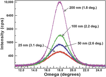
Therefore, in the two-step process, after preliminary RF plasma etch of the Mo electrode with low-energy (30–50 eV) Ar ions, the wafer is heated, and then the first 20-nm-thick AlN film is deposited at an elevated temperature (400–450°C) to enhance adatom mobility. The first stage of the process is also performed with higher nitrogen gas flow to enable the S-gun magnetron to operate in a “deeper” poison mode to promote the nucleation of small grains preferably oriented by the nitrogen basal plain on top. During stage two, the remaining film is deposited at an ambient temperature of about 300°C to restrict the growth of extra-large columnar grains. Regulation of the flux of charged species, substrate temperature, and gas content during deposition enabled formation of films with a controllable stress gradient as well as in-plane stress. X-ray rocking curves of 200-, 100-, 50-, and 25-nm-thick AlN films show (Figure 13) that, while the amplitude of the peaks was essentially reduced in the thinner films, the base shape of the curves remained identical (indicating identical nucleation and growth conditions), and the degree of crystallographic orientation remained notably high with a FWHM of 1.8° and 3.1° for 200-nm and 25-nm, respectively. High resolution TEM analyses have shown that these ultrathin films have a fine columnar texture and a continuous lattice microstructure within a single grain from the interface with the Mo layer through to the AlN surface, thus confirming the presence of a strong orientation even in the 25-nm-thick film.Reference Felmetsger, Laptev and Graham65
X-ray rocking curves of AlN films deposited on Mo electrodes using a two-step sputtering process (numbers in parentheses are values of full width at half maximum obtained for each film thickness).Reference Felmetsger, Laptev and Graham65

Preliminary characterizations of these ultrathin AlN films performed in collaboration with Polytechnic University of Madrid (solidly mounted BAW resonators),Reference Iborra, Clement, Capilla, Olivares and Felmetsger62 University of California–Berkeley (Lamb wave resonators),Reference Chih-Ming, Ting-Ta, Felmetsger, Hopcroft, Kuypers and Pisano68 and University of Pennsylvania piezoelectric nanoelectromechanical actuators)Reference Sinha, Wabiszewski, Mahameed, Felmetsger, Tanner, Carpick and Piazza10, Reference Sinha, Wabiszewski, Mahameed, Felmetsger, Tanner, Carpick and Piazza69 validate the study’s potential as a technological base by which to further increase operation frequency and overall performance of different types of electroacoustic devices.
Conclusions
This article reviewed the state-of-the-art in the development of AlN microelectromechanical systems (MEMS) technology with a focus on radio frequency (RF) applications. The thin-film bulk acoustic resonator (FBAR), de facto one of the largest MEMS industry successes, has made AlN thin-film technology widely available and has enabled a broad set of activities in AlN MEMS. Examples of this development are the work on contour-mode resonators and the integration of AlN devices with a complementary metal oxide semiconductor (CMOS). AlN stands out as a preferred candidate for the synthesis of merged MEMS-CMOS silicon chips that will enable the “More-than-Moore” vision. The use of merged CMOS and AlN MEMS for interfacing with the environment rather than just scaling CMOS technology (according to Moore’s law) will possibly lead the next revolution in the integrated circuit industry. It is also strongly believed that new activities in engineering and scaling of the AlN films will further enhance the range of applicability of this technology.
Acknowledgments
The authors would like to thank all the students and postdoctoral researchers that work in Piazza’s laboratory and the researchers of the Sandia microresonator team. Sandia National Laboratories is a multi-program laboratory managed and operated by Sandia Corporation, a wholly owned subsidiary of Lockheed Martin Corporation, for the US Department of Energy’s National Nuclear Security Administration under contract DE-AC04–94AL85000.