

I. INTRODUCTION
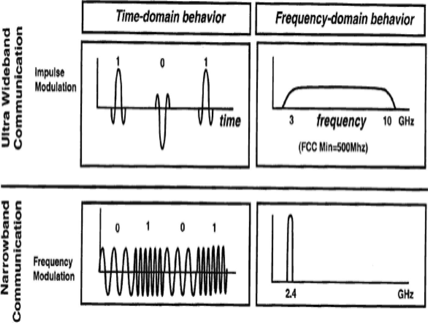
Ultra-wideband (UWB) communication system promises high bandwidth (BW), reduced fading from multipath propagation and low-power requirements. Since 2002, the Federal Communications Commission (FCC) has authorized the use of several frequency bands 0–960 MHz, 3.1–10.6 GHz, and 22–29 GHz for new UWB transmissions. UWB signal is defined as a signal with a fractional BW >0.2 or a signal that occupies more than 500 MHz of spectrum. Thanks to the large BW, UWB is a very promising technology for short-range wireless communications with high data rates, as well as radar and geo location applications, unrealizable in narrowband systems. However, compared to traditional systems, there are many new challenges involved in designing UWB systems, such as antenna design, interference, propagation, channel effects, modulation, and coding methods. One of the main difficulties relies on the emission limits stipulated by the FCC (e.g., 41.3 dBm/MHz within the frequency range 3.1–10.6 GHz). The modern wireless application demands easy to carry devices. Mobility demands small size of devices for modern day wireless gadgets. Wireless communications have been growing with an astonishing rate over the past few years and wireless terminals for future applications are required to provide diverse services. This rising demand prompts the needs for antennas able to cover multiple BWs or an ultra-wide BW for various systems [1, Reference Pan, Huang and Horng2]. There is difference in the modulation schemes in UWB and narrowband communication as shown in Fig. 1.
Difference between UWB and narrowband.

In literature, various methods are discussed to design UWB antenna. Defected Ground Structure (DGS) is also reported in many papers for support of UWB response. In [Reference Naser-Moghadasi, Ebadifallah, Katouli and Sadeghzadeh3], Moghadasi et al. proposed the periodic defected ground structure for UWB response of antenna. In [Reference Hosseini, Altasbaf and Forooraghi4], loaded defected ground structure UWB antenna is proposed by the author. Many other designs [Reference Wu, Kang, Chen and Tarng5, Reference Amert and Whites6] are also proposed for UWB technology. Recent research on UWB antenna is planar technology as they are more practical in term of manufacturing and integration with the entire system [Reference Pan7–Reference Suma, Raj, Joseph, Bybi and Mohanan11].
In this paper, the design of the printed monopole antenna is proposed. By cutting the rectangular patch in stairs-like structure UWB operations for a printed monopole antenna can be easily obtained. The proposed antenna looks like as to have stairs-like patch and having a flower-shaped defected ground structure is referred to as the stair-shaped UWB antenna in this study. Details of the antenna and effect of changing ground shapes, materials, and position of the radiating patch are described in Section II.
II. PROPOSED DESIGN
The dimensional specification of the proposed antenna with the defected ground structure is shown in Fig. 2. The DGS has equal length and width of 16 mm, radius r has the value of 3 mm. The central radius is denoted by R, which is about 3.16 mm.
Defected ground structure design of the proposed antenna.
High Frequency Structure Simulator (HFSS) simulator is used to compute results for the proposed design. The performance of the proposed design is defined in terms of return loss (s11 dB) versus frequency graph. The proposed antenna is optimized in terms of dimensions of staircase patch to achieve UWB response of antenna. This antenna matches properly in the frequency range of 3.2–9.2 GHz. The dimensional description of the radiating patch is shown in Fig. 3, and it describes that the radiating patch has the stairs-like structure. The proposed antenna is printed on FR4 substrate having permittivity of 4.4 and the dielectric loss tangent value of 0.02. The substrate is having dimensions of 30 × 30 mm2. with thickness 1.2 mm. A 50-Ω microstrip line is used to excite the antenna. The width of the microstrip line is about 4 mm. The antenna performance with the ground size of 10 × 30 mm2 is shown in Fig. 4. To improve the impedance matching performance of planar monopole antenna without introducing any size or expense increase, notches are introduced.
Antenna patch design specifications.
Antenna performance with ground size of 10 × 30 mm2.
III. RESULTS AND DISCUSSIONS
The realized antenna achieved an operating BW (VSWR 2) ranges from 3.5 to more than 9.2 GHz as shown in Fig. 5 measured at transfer function and constant group delay within the operating band except notched bands make the proposed antenna suitable for being used in practical UWB applications. To improve the BW of the antenna, different types of notches are cut as shown in Fig. 6 and the stairs have been introduced in the design to enhance the BW of antenna.
Antenna performance with DGS.
Different notch designs.
HFSS tool is used to simulate the proposed design. The current distribution is explained by Fig. 7. It shows that the current distribution is at radiating edges of the patch, so stair case helps in broadband performance of the proposed antenna.
Electric field distribution.
The radiation patterns for the proposed antenna are shown in Fig. 8.
Radiation pattern for the proposed antenna (the above figure defines the radiation pattern measured as the total, and the below figure mentions the theta component of the electric field to draw the pattern).
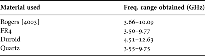
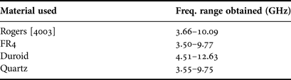
The performance of the proposed antenna for different materials is shown in the following graph. The materials used are FR4, Rogers [4003], quartz, and Duroid. In simulation results, Duroid 5880 proves to be the best materials for the proposed design to achieve an enhanced BW and better mechanical characteristics than using air. Figure 9 and Table 1 show the frequency range obtained for different materials.
Comparison graph for different materials.
Characteristics of the proposed antenna for different materials.
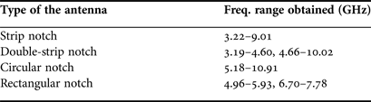
The different notches cut from the radiating patch have also shown a great impact on the antenna performance as shown in Fig. 10. The shapes of the notches are discussed in Fig. 6. Rectangular notch antenna can operate in 4.96–5.93 and 6.70–7.78 GHz bands. Circular notch has a small effect on the lower edge frequency, while it increase the upper edge frequency of the operating band, and the antenna can provide a range from 5.18 to 10.91 GHz. To enhance the BW further, the strip notch is cut, which provides a BW of 5.79 GHz. With the help of double-strip notch, antenna can operate in 3.19–4.60 and 4.66–10.02 GHz bands.
Comparison graph for different notches cut from the radiating patch.
The following figures represent the simulation result of different notches cut from the staircase patch
The characteristics of the given antenna for different notches cut from the patch with frequency range obtained for the respected structures are shown in Table 2.
Characteristics of the proposed antenna for different notches.
It has been observed that the proposed structure of the antenna with double-strip notch shows an extra advantage of performing in the dual-UWB character, which is shown in Fig. 10. As shown above in Figs 6, 9–12 describe the comparison between the simulated and fabricated results. It can be observed from the above figures that simulation and measured results are approximating similarly. Next, the radiation patterns in the two-dimensional (2D) rectangular plot are shown in Fig. 13.
(a), (b) Fabricated antenna with the staircase design; (c), (d) antenna with the circular notch and its ground plane; (e), (f) antenna with the double-strip notch and its ground plane; (g), (h) staircase antenna with the flowery DGS ground structure.
Simulated and measured results for different notches cut from the radiating patch.
Far-field radiation patterns in the 2D rectangular plot.
IV. CONCLUSION
The UWB operation of a stair-shape monopole antenna with the defected ground structure has been demonstrated. Designed antenna which is also suitable for dual-UWB operations in 3.19–4.60 and 4.66–10.02 GHz has been studied and good antenna performances of the operating frequencies across the wider frequency band have been obtained. The effects of varying different parameters have also been studied.
 Sukhdeep Kaur received B.Tech. (Eng.) degree in ECE in 2001 from Amravati University and M.Tech. degree from GNE, Ludhiana in 2008. She is pursuing her Ph.D. from Thapar University, Patiala. She is currently working as an Associate Professor and HOD in ECE Department at JCDMCOE, Sirsa. She has published many papers in National and International Journal/Conferences. Her main research interest includes antennas and Wireless Communication.
 Rajesh Khanna received B.Sc. (Eng.) degree in ECE in 1988 from REC, Kurukshetra and M.E. degree in 1998 from Indian Institute of Science, Bangalore. He was with Hartron R&D centre till 1993. Until 1999, he was in AIR as AS Eng. He is currently working as a Professor and HOD in the ECED at Thapar University, Patiala. He has published 80 papers in National and International Journal/Conferences. He has worth Rs. 1.5 crore projects to his credits. His main research interest includes antennas, Wireless Communication, MIMO, and FFT.