I. INTRODUCTION
The demand of planar monopole antenna in microwave communication is increasing day by day due to its virtues like inexpensive, small volume, facile fabrication, and facile integration with microwave circuits. These antennas also provide omnidirectional radiation pattern and pure polarization [Reference Luxia, Huiping, Xueguan and Ying1–Reference Ellis, Zhao, Wu, Nie and Liu3]. The bandwidth of the planar monopole antenna is enhanced by embedding slots and notch on the ground plane [Reference Ghaderi and Mohajeri4–Reference Liu, Zhong and Esselle6]. These slots and notches modify the resonance frequency of the fundamental mode (TM 10 or TM 01) and higher order modes (TM 12, TM 20). Due to overlapping of these modes, wide impedance bandwidth is realized [Reference Liu, Zhong and Esselle6–Reference Deshmukh and Ray8]. Slots on the ground plane also change the current distribution, introduce anti-resonant property, and nullify the effect of the ground plane. These slots also improve the radiation property of the planar antenna [Reference Lu, Chattha and Cao9]. Feeding method like tapered feed, asymmetric feed (offset fed), also enhances the bandwidth of planar monopole antenna [Reference John, Evans, Ammann, Modro and Chen10, Reference Manohar, Kshetrimayum and Gogoi11].
In addition, deformation in shape of the patch (arch shape, stepped shape, cross shape, checkered shape, U shape, and deformed elliptical shape) and the ground plane of the planar monopole antenna is another approach to achieve broad bandwidth. Due to the deformation of the patch and ground plane, the new edge of fringing fields arises, or new resonance frequencies are generated near fundamental frequency [Reference Lu and Yeh12–Reference Lau, Li and Luk20].
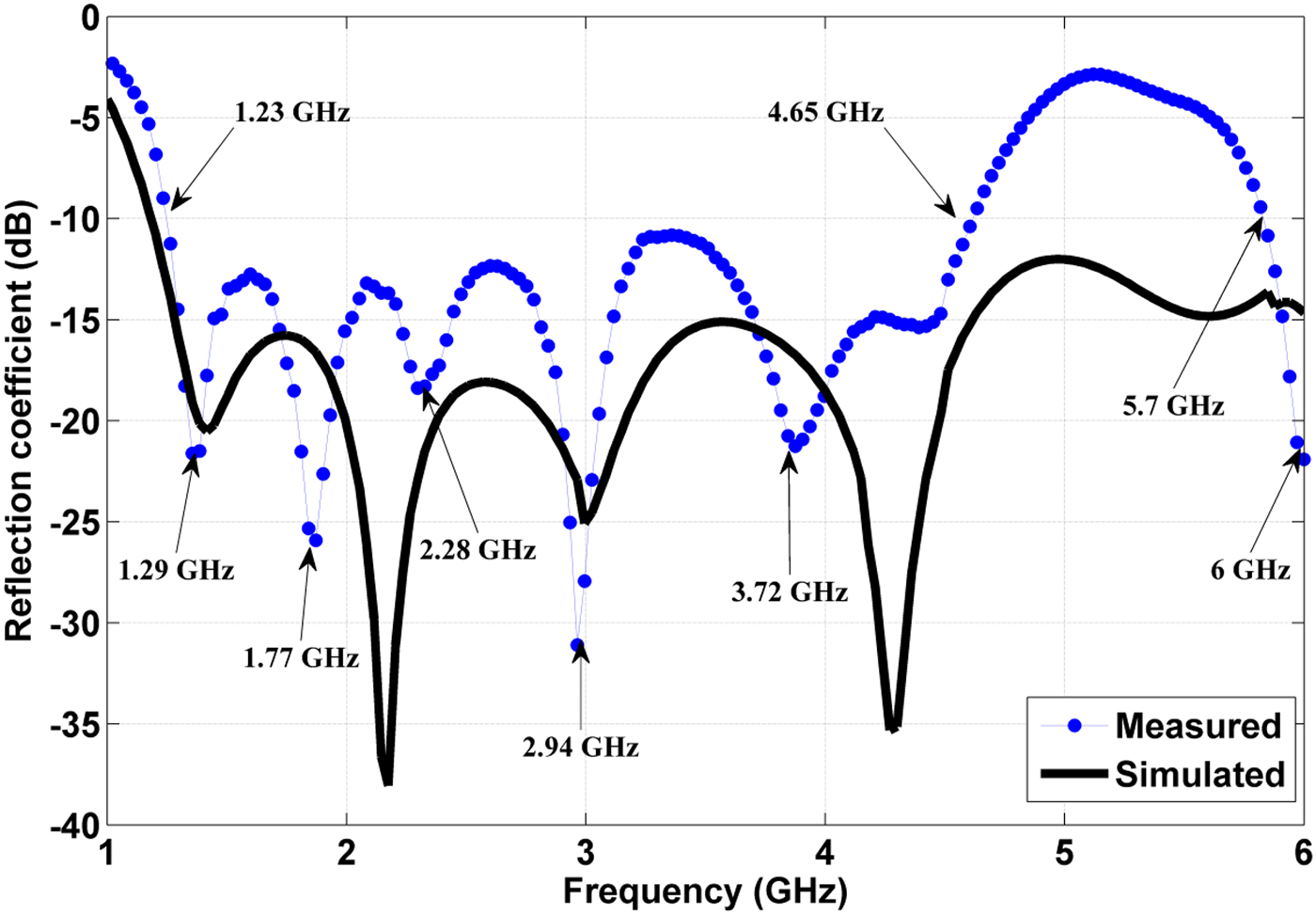
In this communication, we propose a novel design of Scarecrow-shaped antenna for broadband applications. Wide impedance bandwidth has been achieved by introducing elliptical notch on the top edge of the partial ground plane. In addition, two symmetrical parasitic slots have incorporated on the corners of the ground plane. Due to these parasitic slots, the VSWR and return loss characteristics of the antenna have been improved. The proposed configuration offers the impedance bandwidth of 116.32% from 1.23 to 4.65 GHz for S 11 < − 10 dB. This antenna exhibits the omnidirectional radiation pattern in H-plane and bidirectional pattern in E-plane. The proposed configuration is favorable for many wireless applications, such as personal communication service (1.85–1.99 GHz), ISM (2.402–2.48 GHz), GSM (1.71–1.88 GHz), and wireless communication services (2.345–2.36 GHz). Details of the proposed antenna design, simulated current distributions, the evolution of proposed antenna, and a parametric study are discussed.
II. ANTENNA GEOMETRY
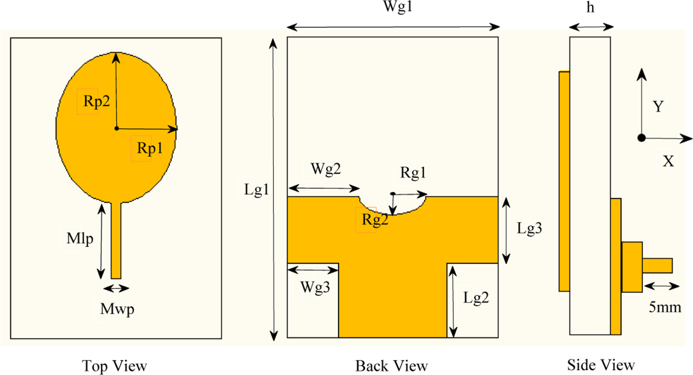
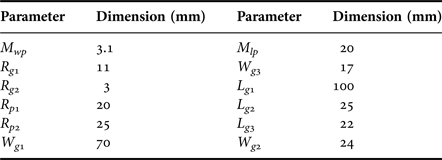
The two-dimensional geometry of the Scarecrow-shaped antenna is illustrated in Fig. 1. This proposed antenna is placed on X–Y plane. A simple configuration proposed consists of an elliptical radiating patch, 50 Ω microstrip feed line, and modified partial ground plane. The parameters of elliptical patch are nominated as R p1 and R p2 as semi-minor axis radius and semi-major axis radius, respectively. This radiating element has been designed for f r = 1.79 GHz, which is determined by the resonance frequency equation of ellipse (equations (2) and (3)). The feed line parameters are denoted by M wp and M lp as width of the feed line and length of the feed line, respectively. This feed line has terminated on radiating element. Modified partial ground plane comprises elliptical notch and two symmetrical parasitic slots. The elliptical notch has been etched on the top edge of the partial ground plane and below the junction where radiating element and feed line are Boolean added. It plays an important role in impedance matching. The parameters of elliptical notch are chosen as R g1 and R g2 as semi-major axis radius and semi-minor axis radius, respectively. The two symmetrical parasitic slots are incorporated at the corners of ground plane, and these slots improve the return loss characteristic and decrease the VSWR of the antenna. The parameters of parasitic slots are denoted by L g2 and W g3. The proposed antenna is fabricated on FR-4 substrate with a dielectric constant of 4.4, tangent loss of 0.02, and thickness of 1.6 mm. The overall volume of the antenna is 100 × 70 × 1.6 mm3. This structure is excited by coaxial feed technique. In simulation, radius of the inner conductor has been chosen (0.7 mm) and thickness of the outer conductor is selected (0.02 mm). The inner conductor of the coaxial cable has been connected with the microstrip line. Thickness of the copper conductor (top and bottom layers) is taken (0.035 mm). To realize the wide impedance bandwidth, the dimensions of all the elements (radiating element, feed line, elliptical notch, and parasitic slots) have been optimized. The optimal dimensions with parameters of proposed antenna are listed in Table 1.
Schematic configuration of Scarecrow patch antenna.

Optimized dimensions of the proposed antenna.

III. EVOLUTION OF THE ANTENNA
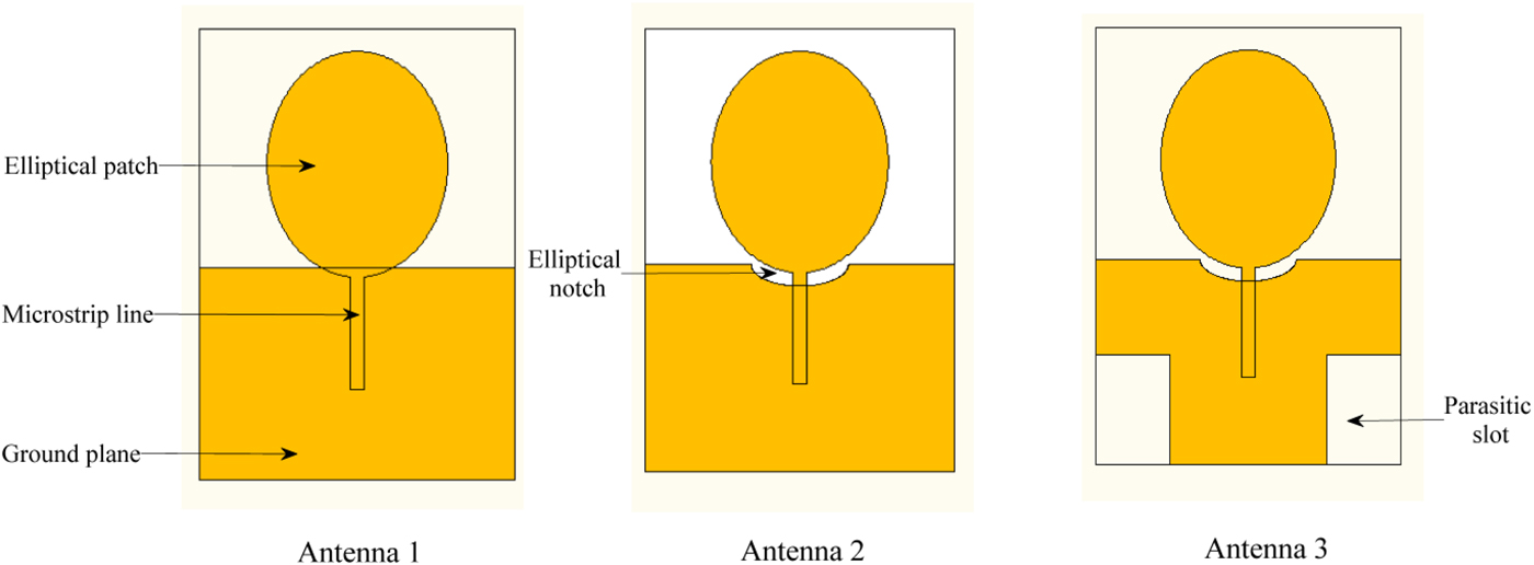
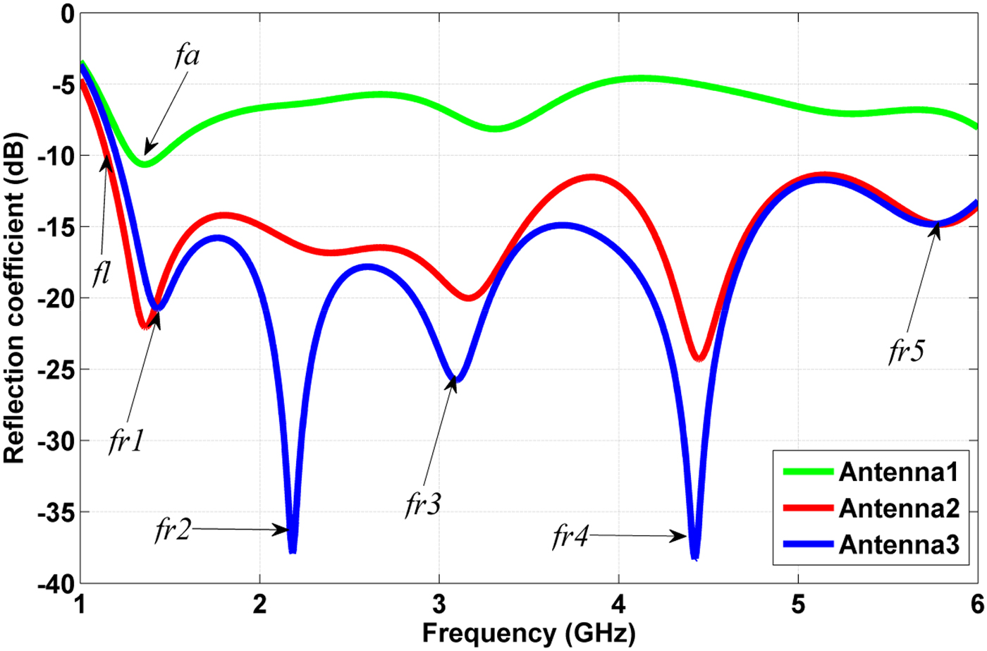
In this section, evolution of the proposed antenna has been discussed. Figure 2 illustrates the development of Scarecrow-shaped antenna. The shape of radiating patch and feed line are identical for antennas 1, 2, and 3. These two elements are designed on the top layer of the FR-4 substrate. Only ground plane has been modified in the succeeding stage. The comparison of S 11 characteristics of the antennas 1, 2, and 3 has been displayed in Fig. 3. Firstly, antenna 1 (without modification of ground plane) has been investigated numerically that exhibits the poor impedance bandwidth while it is resonating in one frequency band around f a = 1.29 GHz. In rest of the frequency band, antenna 1 shows its inductive nature. In electrically small antennas, the shape and size of the ground plane and position of the radiating patch change the performance of the printed planar antennas. It has been investigated that in many research articles, slot introduces the capacitive effect on the antenna and it also compensates the inductive behavior of the antenna. Moreover, for bandwidth enhancement, an elliptical notch has been incorporated on top edge of the partial ground plane. A positive impact of elliptical notch has been investigated on the S 11 characteristic of antenna 2. This element introduces the capacitive effect on antenna, which nullifies the inductive behavior of antenna 1. An antenna with elliptical notch (antenna 2) shows the impedance bandwidth of 133.33% from 1.15 to 6 GHz for S 11 < − 10 dB. In the next step, two symmetrical slots have been introduced on the corners of the partial ground plane. These symmetrical parasitic slots improve the VSWR characteristic of the antenna and also introduce new resonating frequency f r2. Antenna 3 also exhibits five resonating frequencies f r1, f r2, f r3, f r4, and f r5. It exhibits a bandwidth of 130.84% from 1.27 to 6 GHz for S 11 < − 10 dB. It has also been investigated from Fig. 3 that the lower cut-off frequency f l is slightly affected due to modification in the ground plane.
Evolution of the proposed antenna.

Comparison of simulated S 11 characteristics of the antennas 1, 2 and 3.

IV. PARAMETRIC STUDY
The parameters of the antenna have been optimized to realize the wide impedance bandwidth. In this section, the impact of parameters (R g1, R g2, L g2, and W g3) on the frequency response of the antenna has been investigated. These parameters affect the impedance bandwidth of the antenna and the position of the resonating frequencies.
A) Effect of elliptical notch parameters (R g1 and R g2)
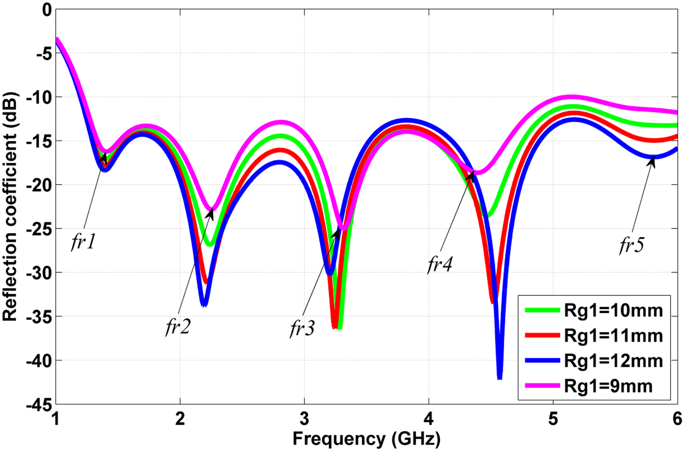
Figure 4 demonstrates the effect of R g1 (semi-major axis radius of the notch) on the simulated S 11 characteristic of the proposed antenna. It can be investigated that the parameter R g1 does not affect the impedance bandwidth of the antenna, while it has modified the position of resonance frequencies (f r2, f r3, f r4, and f r5.) and impedance matching at these frequencies. Due to change in the length of R g1, the path length of the current is also modified. Due to this reason, resonance frequencies are shifted. The range of this parameter (R g1) has been varied from 9 to 12 mm. It has been investigated from Fig. 4 that the value return loss has increased at resonating frequencies (f r1, f r2, f r4, and f r5) by increasing the value of R g1. The uneven variation of return loss has been observed at resonance frequency f r3. This parameter alters the electromagnetic coupling effect between ground and radiating patch. Due to this reason, the value of return loss has been changed at resonating frequencies. The maximum value of return loss is found at frequency f r4 for R g1 = 12 mm. On increasing the value of R g1, resonating frequencies f r2 and f r3 have been shifted left, while resonance frequency f r4 is shifted right. It can also be seen from Fig. 4 that impedance bandwidth of the antenna has been deteriorated for R g1 <9 mm.
The simulated S 11 characteristic of the proposed antenna for different values of R g1.

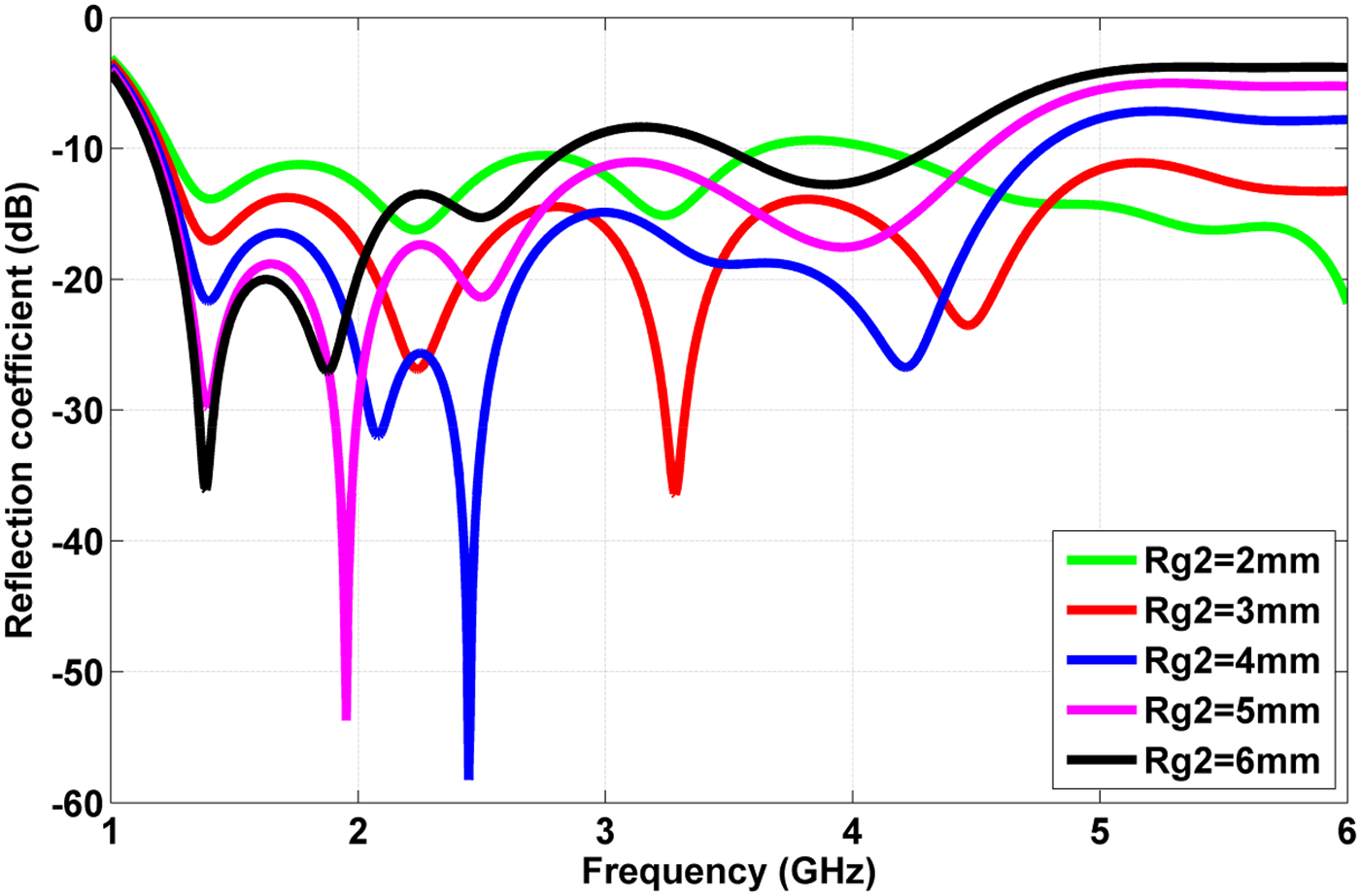
Figure 5 illustrates the simulated S 11 characteristic of the antenna with various values of R g2 (semi-minor axis radius of the notch). It can be seen from Fig. 5 that the parameter R g2 significantly affects the impedance bandwidth of the antenna. It alters the mutual coupling between radiating patch and ground plane. The value of R g2 has been varied from 2 to 6 mm. The best impedance matching is found for R g2 = 3 mm with the impedance bandwidth of 132.89%. It can also be investigated that impedance matching is worst for R g2 <3 mm and R g2 >5 mm. This is because of less electromagnetic coupling between ground plane and radiating patch. It has also been observed from Fig. 5 that this parameter alters the value of return loss at resonating frequencies.
The simulated S 11 characteristic of proposed antenna for different values of R g2.

B) Effect of size of parasitic slot (L g2 and W g3)
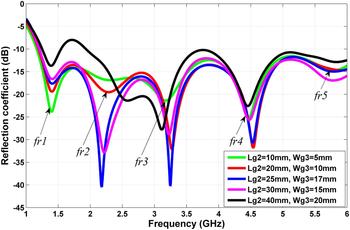
The size of parasitic slots affects the electromagnetic coupling between the defected ground plane and radiating element. It also alters the position of resonance frequencies and the impedance matching resonance frequencies. On increasing the size of parasitic slots, the impedance matching at resonance frequency f r1 is reduced, while uneven impedance matching has been investigated at resonance frequencies f r2, f r3, f r4, and f r5. Figure 6 shows the simulated S 11 characteristic of the proposed antenna for various sizes of the parasitic slots. For the larger size of the parasitic slots, i.e. L g2 = 40 mm and W g3 = 20 mm, the impedance bandwidth of the antenna has been deteriorated. It is because of less mutual coupling between radiating patch and ground. The best impedance matching has been found for size L g2 = 25 mm and W g3 = 17 mm. It has also been investigated from Fig. 6 that the size of the parasitic slot changes the value of return loss in the entire spectrum (1–6 GHz).
The simulated S 11 characteristic of proposed antenna for different values of L g2 and W g3.

V. RESULT AND DISCUSSION
A) S 11 characteristic
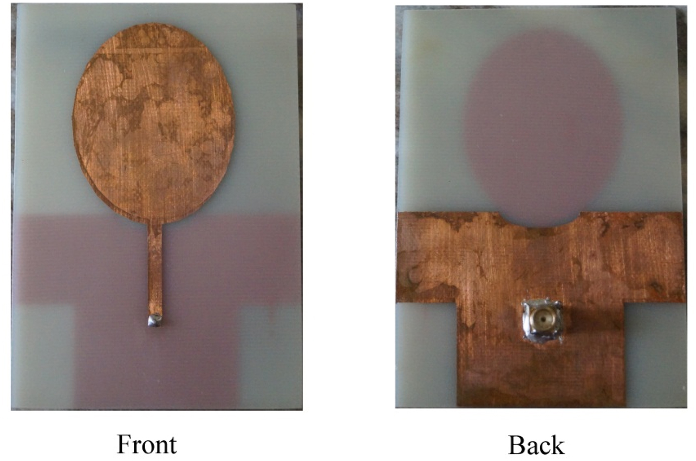
The photograph of the fabricated Scarecrow antenna is shown in Fig. 7. Firstly, the proposed antenna has been analyzed using CST Microwave Studio. After numerical analysis, the S 11 characteristic of the antenna has been measured in the frequency band 1–6 GHz using vector network analyzer N9923A. The comparison between measured and simulated S 11 characteristic of the proposed antenna has been depicted in Fig. 8. It can be seen that this antenna is resonating at frequencies 1.29, 1.77, 2.28, 2.94, 3.72, and 6 GHz. The proposed antenna has exhibited the impedance bandwidth of 116.32% from 1.23 to 4.65 GHz for |S 11 | < − 10 dB. Another resonating band has been found from 5.7 to 6 GHz. Impedance matching has been deteriorated in the frequency band 4.65–5.7 GHz. Some mismatch between measured result and simulated result has been observed due to ground plane effect, SMA connector, and fabrication tolerance. The first resonating frequency has been found at 1.29 GHz. It has also investigated that resonating frequencies are generated because of the elements (radiating patch and ground plane) of the proposed antenna. The frequency 1.29 GHz has been generated because of the partial ground plane. The detail about resonating frequencies (1.29, 1.77, 2.28, 2.94, and 3.72 GHz) has been discussed in the current distribution section.
Fabricated Scarecrow patch antenna.

Comparison of measured and simulated return loss of Scarecrow patch antenna.

The lower cut-off frequency of the proposed monopole antenna depends on the length of the radiating patch. Lower cut-off frequency f l of the proposed antenna is calculated by the given equation [Reference Ray and Ranga21, Reference Agrawall, Kumar and Ray22].
 $$f_l = {{70} \over {(L + r + p)k}}\; {\rm GHz,}$$
where L = 50 mm that is equal to the length of cylindrical monopole, r = 5 mm, which is a radius of the cylindrical monopole antenna (2πrL = πab, where a = 25 mm and b = 20 mm) and p = 0 mm; k = 1.15 is constant. The measured and calculated values of lower cut-off frequency f l are 1.23 and 1.14 GHz, respectively. The second resonating frequency is found at 1.77 GHz and it has been generated because of the radiating patch. This frequency or mode (TM 11) can be calculated by the following equations [Reference Agrawal, Vakula and Sarma23].
 $$\eqalign{ a_{eff} &= a\left[ 1 + \displaystyle{{2h} \over {\pi \varepsilon _r a}}\; \left\{ {\rm ln}\left( {\displaystyle{a \over {2h}}} \right) + (1.41\varepsilon _r + 1.77)\right.\right. \cr &\left. + \displaystyle{h \over a}\; (0.268\varepsilon _r + 1.65) \right]^{1/2} \;,}$$
 $$\; \; f_{11}^{e,o} = \displaystyle{{15} \over {\pi ea_{eff}}} \sqrt {\displaystyle{{q_{11}^{e,o}} \over {\varepsilon _r}}}, $$
 $$q_{11}^e = - 0.0049e + 3.7888e^2 - 0.7278e^3 + 2.314e^4, $$
 $$q_{11}^o = - 0.0063e + 3.8316e^2 - 1.1351e^3 + 5.2229e^4. $$
where a is the semi-major axis, h is the height of the substrate, ε r is the dielectric constant of the substrate, e is an eccentricity of the ellipse, and a eff is an effective radius. The calculated and measured values of the second resonance frequency are 1.79 and 1.77 GHz. Small error of 1.11% has been found between calculated and measured second resonance frequencies. It is because of slots, notch, and effect of the ground plane.
B) Input impedance
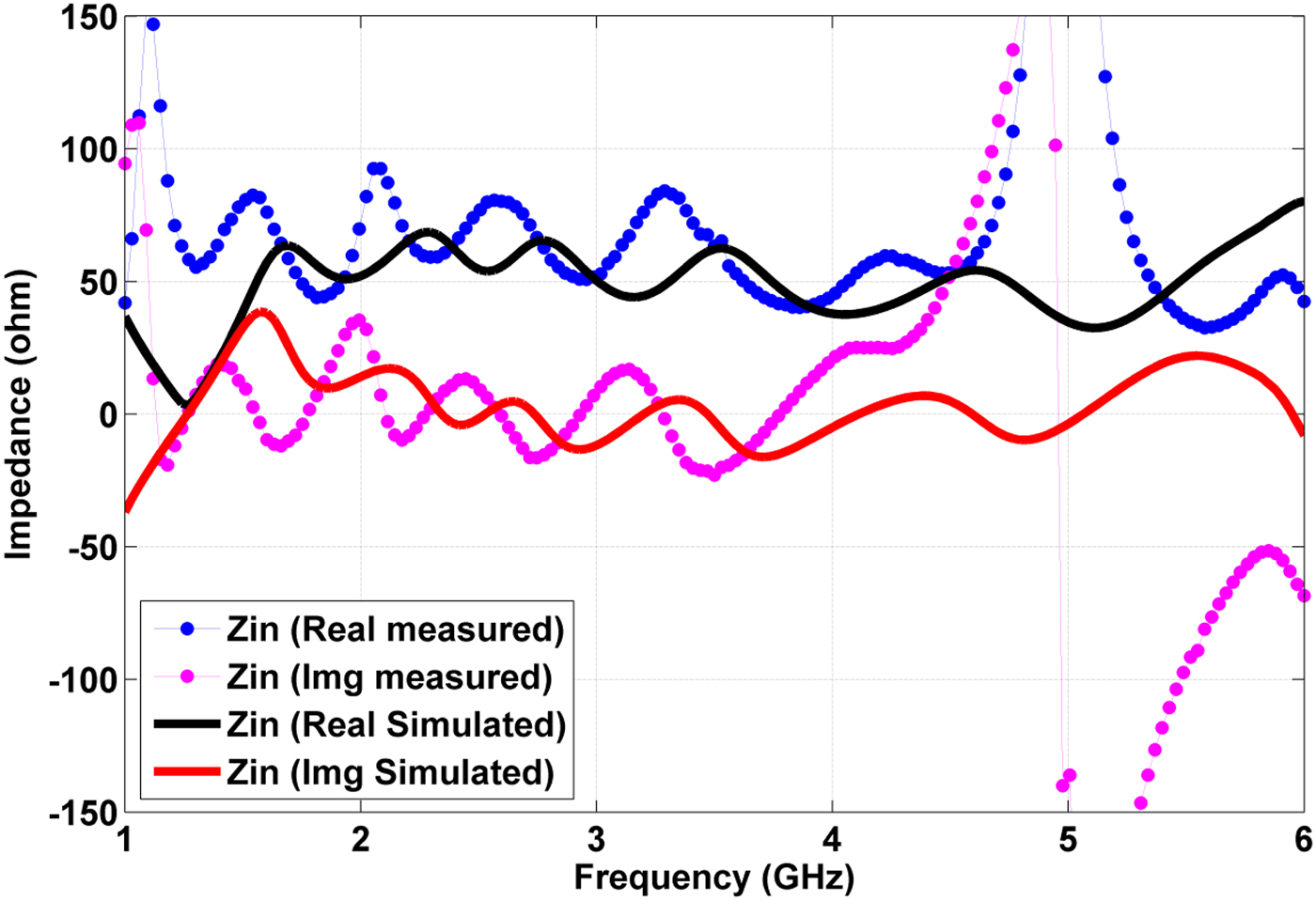
The comparison of the measured and simulated input impedance (Z in) of the proposed antenna has been displayed in Fig. 9. At the resonating frequencies, the reactance of the antenna is zero and antenna impedance is equal to the real part of the input impedance. In the frequency band 1.2–4.5 GHz (Fig. 9), measured input resistance fluctuate around 60 Ω, while simulated input resistance has oscillated around 50 Ω. In the frequency band 4.8–5.2 GHz, the measured input resistance is high because of the ground plane effect. At frequency 5 GHz, antenna behaves as a parallel resonator because the resistance of the antenna is quite high (near 200 Ω) and reactance is zero. Figure 9 also shows the comparison of measured and simulated imaginary part (Z in(imaginary)) of the input impedance (Z in). It has been investigated that the measured reactance of the antenna oscillates around 0 Ω in the frequency band 1.2–4.3 GHz, while simulated reactance has varied around 0 Ω in the entire frequency band (1–6 GHz).
Variation of real and imaginary parts of input impedance Z in.

C) Current distribution
Simulated surface current distributions at resonance frequencies (1.29, 1.77, 2.28, 2.94, and 3.72 GHz) of the proposed antenna are illustrated in Fig. 10. By investigating the simulated current distribution, current vectors are not only distributed on the patch but also on the ground plane. It has also been found that the surface current distribution is symmetric about the y-axis at each resonating frequency. By inspecting the current patterns, the first resonance frequency f 1 = 1.29 GHz has been produced because of the ground plane. At this frequency, the current vectors have distributed along the periphery of the modified partial ground plane. The fundamental frequency f 1 can be determined by the following equations:
 $$L_{f1} = L_{g2} + W_{g3} + L_{g3} + W_{g2} + L_{slot}, $$
 $$L_{slot} = \displaystyle{{\pi R_{g1} R_{g2}} \over 4},$$
 $$\; f_1 = \displaystyle{c \over {L_{f1\;} \sqrt {\varepsilon _r}}} \;, $$
where L f1 is the length. The calculated value of f 1 is 1.255 GHz. The small difference between measured and calculated values of fundamental frequency has been found. It can be seen from Fig. 10 that second resonating frequency has been developed by the radiating patch. At second resonating frequency f 2 = 1.77 GHz, one half-wavelength variation of current vectors has been investigated along the elliptical periphery of the patch. This frequency f 2 has been determined by the resonance frequency equations (2)–(5) of ellipse [Reference Agrawal, Vakula and Sarma23]. The third resonating frequency (higher order mode) f 3 = 2.28 GHz has been developed by the side edge of the ground plane and f 3 is calculated by the following equations:
 $$L_{f3} = L_{g2} + W_{g3} + L_{g3}, $$
 $$\; f_3 = \displaystyle{c \over {L_{f3\;} \sqrt {\varepsilon _r}}} \;, $$
where L f3 is the length. The calculated value of f 3 is 2.23 GHz. The fourth resonating frequency f 4 = 2.94 GHz has been produced because of the top edge and side edge of the ground plane. This frequency f 4 is determined by succeeding the equation:
 $$L_{f4} = L_{g2} + W_{g3}, $$
 $$f_4 = \displaystyle{c \over {L_{f4\;} \sqrt {\varepsilon _r}}}. $$
Simulated surface current distribution of proposed antenna at frequencies f 1 = 1.29 GHz, f 2 = 1.77 GHz, f 3 = 2.28 GHz, f 4 = 2.94 GHz, and f 5 = 3.72 GHz.

The calculated value of frequency f 4 is 3.10 GHz. It has been observed that the harmonics of second resonating frequency is also present in the spectrum. The harmonics of f 2 is determined by nf 2 where n is a positive integer. The frequency f 5 is nearly equal to 2f 2. At fifth resonating frequency f 5 = 3.72 GHz, two exact half-wave variation of current vectors has been found along the elliptical periphery of the patch.
D) Far-field pattern
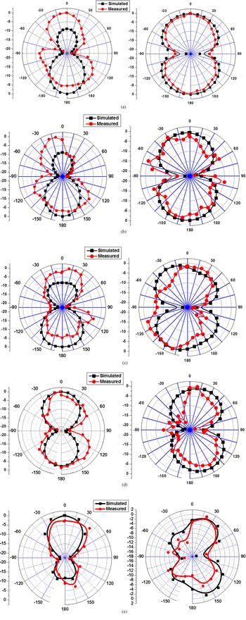
Radiation patterns of the proposed antenna have been displayed in Fig. 11. Far-field patterns of the proposed antenna have been simulated and measured in H-plane and E-plane with 10° increment at frequencies 1.29, 1.77, 2.28, 2.94, and 3.72 GHz. At frequency 1.29 GHz, a good omnidirectional pattern has been found in H-plane, while bidirectional pattern is observed in E-plane. E-plane measured result differs from the simulated result because of measurement, fabrication error, and radiation from coaxial cable at lower frequencies. At frequencies 1.77, 2.28, 2.94, and 3.72 GHz, distorted bidirectional pattern (measured) has been found in E-plane. At frequencies 1.77, 2.28, and 2.94 GHz, quasi-omnidirectional pattern has been investigated in H-plane. At higher frequency, the measured results differ from simulated results due to the presence of higher order modes. These higher order modes have been generated by the feed line, ground plane, and patch. Finally, these modes have been mixed and produce complicated modal distribution. At frequency 3.72 GHz, omnidirectionality has been lost in H-plane. It may be because of higher order modes.
Far-field patterns (E-plane (left), H-plane (right)) of proposed antenna at frequencies (a) f 1 = 1.29 GHz, (b) f 2 = 1.77 GHz, (c) f 3 = 2.28 GHz, (d) f 4 = 2.94 GHz, and (e) f 5 = 3.72 GHz.

VI. CONCLUSION
A novel design of the Scarecrow-shaped patch antenna for broadband application has been investigated in this paper. We have incorporated elliptical notch and two parasitic slots on the partial ground plane to improve the impedance bandwidth and return loss of the antenna. Proposed antenna achieves the bandwidth of 116.32% from 1.23 to 4.65 GHz for |S 11 | < − 10 dB. It has also been investigated that impedance matching is not good in the frequency band 4.5–5.7 GHz due to ground plane effect. Radiation pattern and current distribution at resonating frequencies 1.29, 1.77, 2.28, 2.94, and 3.72 GHz have also been studied. It has been found that radiation patterns are omnidirectional (H-plane) and bidirectional (E-plane) at all frequencies except at 3.72 GHz. For optimization, the effect of parameters on frequency response has also been observed.
 Bhupendra Kumar Shukla received Bachelor of Engineering in Electronics and Communication in 2007 and Master degree in Optoelectronics in 2009 from RGPV University. His main research interest is broadband antenna designing.
 Nitesh Kashyap received the B.E. degree in Electronics Engineering from the Institute of Engineering, Jiwaji University, Gwalior, India, in 2008, the M.E. degree in Microwave Engineering from the Jabalpur Engineering College, Jabalpur, India in 2010, and the Ph.D. degree in Electronics Engineering from the Indian Institute of Information Technology, Jabalpur, India in 2016. Currently he is working as an Assistant Professor in the Maulana Azad National Institute of Technology, Bhopal, India, and his area of interest is antenna designing.
 Dr. Rajendra Kumar Baghel received his B.E. degree in Electronics Engineering from the Rani Durgawati University, Jabalpur, India, in 1991 and M. Tech from MANIT in 1997. He received his Ph.D. in 2008 from MANIT. He is working as a Professor in the Maulana Azad National Institute of Technology, Bhopal, India. His current research interests include low-power VLSI, microelectronics, and optical communication.