Heat-assisted magnetic recording media
Since the first report of high anisotropy granular FePt thin-film media in 2008,Reference Kryder, Gage, McDaniel, Challener, Rottmayer, Ju, Hsia and Erden1,Reference Peng, Klemmer, Ju, Gage, Seigler, Challener, Karns, Zhu, Gokemeijer, Peng, Pelhos, Lu, Rausch, Wu, Li, Hsia, Buechel, Hempstead and Rottmayer2 significant improvements have been made in microstructure, magnetic properties, thermal stack design, and media mechanical performance.Reference Weller and Moser3–Reference Ju, Peng, Chang, Ding, Wu, Zhu, Kubota, Klemmer, Amini, Gao, Fan, Rausch, Subedi, Ma, Kalarickal, Rea, Dimitrov, Huang, Wang, Chen, Peng, Chen, Dykes, Seigler, Gage, Chantrell and Thiele5 Heat-assisted magnetic recording (HAMR) media requirements for 2 and 4 Tbpsi media, from the Advanced Storage Technology Consortium, are shown in Table I.Reference Weller, Parker, Mosendz, Champion, Stipe, Wang, Klemmer, Ju and Ajan4 For the areal density of 4 Tbpsi, the size of ferromagnetic grains in a medium must be ∼4 nm for a sufficient signal-to-noise ratio (SNR). This small volume makes most ferromagnetic materials thermally unstable, as the magnetocrystalline energy K uV becomes comparable to the thermal energy k BT, where K u is the uniaxial magnetocrystalline anisotropy constant, V is the grain volume, k B is the Boltzmann constant, and T is temperature. In order to retain the recorded information for longer than 10 years, K uV/k BT must be larger than 60. This means that a ferromagnetic material with high magnetocrystalline anisotropy such as L10-FePt must be used for ultrahigh density recording.Reference Weller and Moser3
Heat-assisted magnetic recording media requirements for 2 and 4 Tbpsi recording densities.

Adapted from the Advanced Storage Technology Consortium.Reference Weller, Parker, Mosendz, Champion, Stipe, Wang, Klemmer, Ju and Ajan4
Note: μ0M s, saturation magnetization; K u, anisotropy constant; μ0H k, anisotropy field; σHk, anisotropy field distribution;  $\sigma _{{\rm{T}}_{\rm{C}} } $, Curie temperature distribution.
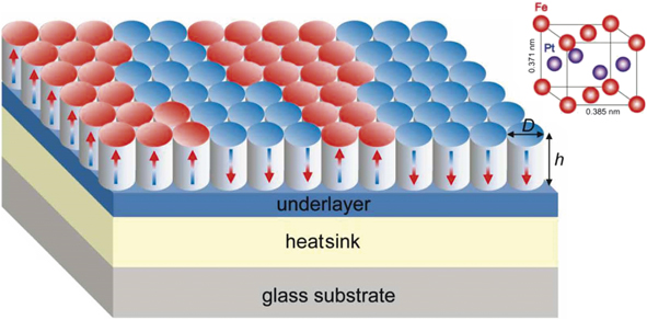
For 2 Tbpsi, the desirable HAMR medium should comprise densely dispersed ferromagnetic grains with magnetocrystalline anisotropy >3.5 MJ/m3, an average grain size of <6 nm, a center-to-center distance of <7 nm, a grain-size distribution <10% and a grain-aspect-ratio h/D > 1.5, where h is height and D is diameter. Such an ideal film structure is schematically shown in Figure 1.Reference Varaprasad, Takahashi and Hono6 In addition, the microstructure should be realized on commercially viable substrates, such as glass. The key factors to control the microstructure of HAMR media are (1) high degree of L10-order in FePt nanograins, (2) strong perpendicular magnetic anisotropy (PMA) with low in-plane magnetic component, (3) columnar grains smaller than 6 nm with a size distribution of less than 10%, and (4) low surface roughness (R a < 0.4 nm, where R a is the arithmetic average roughness) to support low head–media spacing needed for high density recording. Much effort has been expended to optimize the FePt-based nanogranular structure since 2000. Seagate has recently demonstrated significant progress in HAMR areal density, including the latest reported areal density demonstration of 1.97 Tbpsi using FePt-based granular media.Reference Granz, Zhu, Rea, Ju, Thiele, Rausch and Gage7 However, further microstructure optimization is needed to extend the areal density to 4 Tbpsi in the future.Reference Rea, Subedi, Zhou, Saunders, Cordle, Lu, Granz, Czoschke, Hernandez, Jury, Peng, Thiele, Wu, Ju, Rausch, Seigler and Gage8
The ideal structure of a heat-assisted magnetic recording medium for 2 Tbpsi areal density. The L10-FePt grains must grow columnarly separated by a nonferromagnetic segregant. For 2 Tbpsi, column-height-to-grain diameter ratio must be >1.5 and the diameter of the grains must be <4 nm.

FePt-C HAMR media
Watanabe et al.Reference Watanabe, Masumoto, Ping and Hono9 reported one of the earliest works on FePt-based granular film using FePt-Al-O. In the as-sputtered condition, randomly oriented FePt grains of ∼5-nm diameter were uniformly dispersed. However, the structure of the FePt grains was a disordered face-centered-cubic phase (A1) without any crystallographic texture. High-temperature annealing led to L10 ordering, but also caused the coarsening and coalescence of the FePt grains.
Ko et al.Reference Ko, Perumal and Shin10 reported FePt-C granular films with PMA having an average grain size of 4 nm. They cosputtered FePt and C on MgO(001) single-crystalline substrates at 400°C. Since C has little solubility in FePt, it is rejected from FePt nanograins, making the FePt grains magnetically isolated through an intergranular carbon segregant. High-temperature growth promotes L10 ordering and a strong [001] texture develops because of the lattice match between the FePt(001) and MgO(001) planes. The expansion lattice mismatch of about 9.6% causes single variant growth of FePt(001) on MgO(001).
Perumal et al. published the first media-like structure using L10-FePt. They reported FePt-C based PMA granular films with an unprecedentedly narrow size distribution of exchange-decoupled L10-FePt grains as shown in Figure 2.Reference Perumal, Takahashi and Hono11 The average grain size of the L10-ordered FePt was ∼5.5 nm with a 2.3-nm size dispersion. The films were grown by cosputtering Fe, Pt, and C on an MgO seed layer that was predeposited on thermally oxidized Si substrates. Plan-view transmission electron microscope (TEM) images show excellent isolation of the FePt grains with a small size distribution. However, the coercivities of the films were only 8–15 kOe due to the low degree of the L10 order in the FePt grains.
Plan-view and cross-sectional transmission electron microscope bright-field images and magnetization curves of FePt-C granular films with nominal thickness, t, of 6 nm and 10 nm. Up to t = 6 nm, the film grows with a single-layer granular structure, but a second granular layer appears for t > 6 nm and the in-plane component in the magnetization increases for t > 6 nm.Reference Perumal, Takahashi and Hono11

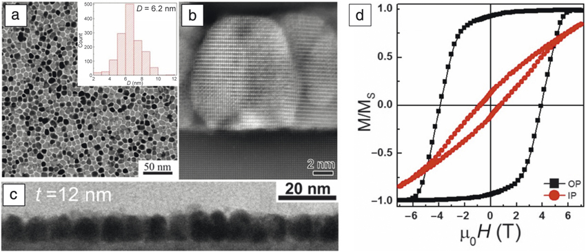
Zhang et al. later succeeded in enhancing the coercivity of the FePt-C granular films to 3.7 T by alloying FePt with Ag.Reference Zhang, Takahashi, Perumal and Hono12 The role of Ag for the enhancement of the coercivity was later found to be due to the diffusion of Ag from the core to the shell based on STEM/EDS investigation.Reference Varaprasad, Takahashi, Wang, Ina, Nakamura, Ueno, Nitta, Uruga and Hono13 Here, the core and the shell correspond to the FePt grains and Ag, respectively. To align the [001] crystal orientation perpendicular to the film, a thin layer of MgO was grown on a Si substrate, followed by sputtering a (FePt)Ag-C magnetic layer. The (FePt)-30.6 vol% C film had low grain-size dispersion, strong [001] texture, and good L10 ordering as shown in Figure 3a–b. Figure 3d shows the magnetization curves for out-of-plane (OP) and in-plane (IP) directions. The film has strong PMA as expected from the strong [001] texture. The perpendicular coercivity (μ0H c) was about 3.5 T and the anisotropy field was about 6.5 T. The estimated K u of the FePt grains was 4.3 × 10⁶ J/m3, which is half of that reported for a bulk L10-FePt. The high K u—much higher than that of currently used media—and μ0H c result from the high degree of L10 order, 0.9. Hitachi Global Storage Technologies reported similar microstructure on glass substrates with a NiTa amorphous heatsink layer.Reference Mosendz, Pisana, Reiner, Stipe and Weller14–Reference Weller, Parker, Mosendz, Lyberatos, Mitin, Safonova and Albrecht16
(a–b) Plan-view and cross-sectional transmission electron microscope bright-field images of FePt-30.6 vol% C films deposited by the compositionally graded process to the nominal thickness of 12 nm. The grain aspect ratio is near 2.0. (c) High-angle annular dark-field image showing a well-ordered L10 structure except near the surface. (d) Magnetization curves show perpendicular magnetic anisotropy film with substantial in-plane component. Note: OP, out-of-plane; IP, in-plane.

Media optimization toward 4 Tbpsi
In order to advance HAMR areal density to 4 Tbpsi, it is necessary to further improve media microstructure, roughness, and magnetic properties, along with the distributions of these parameters, in order to increase signal, reduce noise, and optimize recording performance.Reference Watanabe, Masumoto, Ping and Hono9 In addition, the thermal properties are critical to provide a high thermal gradient and enable a thermally efficient recording process.
Increasing the product of the magnetic moment and the layer thickness, M rt, is vital for good media SNR. A high M rt is only achieved by growing dense, well-separated, columnar grains. Currently, the M rt of HAMR media are significantly (20–30%) lower than those of perpendicular media. As shown in Figure 2, FePt-C tends to form a second layer for thicknesses above 6 nm; however, 8-nm or larger thicknesses, t, are necessary for a high SNR in recorded data. To grow the FePt grains in a columnar shape for thicknesses larger than 6 nm, it is essential to suppress the phase separation between FePt and C in the direction perpendicular to the film plane. One method to achieve this is to use an FePt-C granular film as a seed layer and then grow FePt-SiO2 on top of it since the latter has a smaller driving force for phase separation.Reference Varaprasad, Chen, Takahashi and Hono17 Variations in segregant also were employed by industry to achieve columnar growth.Reference Hellwig18 Varaprasad et al. reported a compositionally graded sputtering process to achieve the columnar growth of FePt grains.Reference Varaprasad, Wang, Shiroyama, Takahashi and Hono19 Optimized growth gave columnar grains with an aspect ratio of 1.9, with the average grain size of 6.2 nm as shown in Figure 3.Reference Pandey, Perumal, Wang, Takahashi and Hono20
The SNR is degraded and jitter noise in data readout is increased by the presence of in-plane components of magnetization, such as that seen where the “IP” curve crosses the M/Ms axis in Figure 3. Unfortunately, all the prototype FePt-C granular media grown on MgO seed layers contain substantial in-plane components, which is attributed to misaligned grains as observed by TEM.Reference Wicht, Neu, Schultz, Weller, Mosendz, Parker, Pisana and Rellinghaus21,Reference Ho, Zhu, Kulovits, Laughlin and Zhu22
Wang et al.Reference Wang, Hata, Takahashi, Sepehri-Amin, Varaprasad, Shiroyama, Schrefl and Hono23 investigated the easy axis distribution in FePt-C media deposited on either a single-crystal MgO substrate or a polycrystalline MgO underlayer in order to clarify the influence of grain boundary and textures of the MgO seed layer. Figure 4 shows TEM images and magnetization curves of these films.Reference Wang, Hata, Takahashi, Sepehri-Amin, Varaprasad, Shiroyama, Schrefl and Hono23 Both films show similar microstructures with average grain size of about 10 nm and grain-size distribution of 1.4 nm. Although the films grown on polycrystalline MgO show strong PMA and H c, the squareness and the gradient of the demagnetization curve of the film deposited on the MgO single-crystal substrate are far better. This indicates that either the angular distribution of the MgO grains or the presence of grain boundaries in the polycrystalline seed layer cause the in-plane component of the magnetization. This suggests that if the misalignment of [001] texture in the MgO seed layer is improved, the easy axis distribution will be substantially improved. However, even if an MgO(001) single-crystalline substrate is used, the in-plane component cannot be completely removed, suggesting additional origins of the misalignment of FePt grains. A recent investigation indicated a correlation between the in-plane component of the magnetization and the carbon concentration, suggesting that the amount of C or possible dissolution of C in FePt also influences the in-plane component.Reference Pandey, Wang, Shiiroyama, Varaprasad, Sepehri-Amin, Takahashi, Perumal and Hono24
Plan-view and cross-sectional transmission electron microscope bright-field images of FePt-C granular film on (a) MgO single-crystal and (b) polycrystalline MgO underlayer. Inset: FePt grain-size distribution, unit in nm. The FePt-C magnetic layer was deposited with the concentration graded process of [FePt-48 vol% C (0.25 nm)/FePt (0.15 nm)]25 to obtain the 10-nm nominal thickness of the FePt-C layer. In-plane and out-of-plane magnetization curves of the FePt-C granular film on (a) MgO single-crystal and (b) polycrystalline MgO underlayer.Reference Wang, Hata, Takahashi, Sepehri-Amin, Varaprasad, Shiroyama, Schrefl and Hono23

High areal recording density in HAMR also requires a narrow Curie temperature distribution  $\sigma _{{\rm{T}}_{\rm{C}} } $. However, FePt growth naturally produces a distribution of grain sizes and, most alarmingly, a distribution of Curie temperatures, possibly caused by each grain having variations in stoichiometry and local ordering. The size distribution itself introduces variation in ordering, where the smaller grains are less ordered, leading to Curie temperature distributions, anisotropy distributions, and thermal capacity variations in the grains.Reference Ju, Peng, Chang, Ding, Wu, Zhu, Kubota, Klemmer, Amini, Gao, Fan, Rausch, Subedi, Ma, Kalarickal, Rea, Dimitrov, Huang, Wang, Chen, Peng, Chen, Dykes, Seigler, Gage, Chantrell and Thiele5,Reference Chapline, Papusoi, Ajan, Dorsey, Desai and Acharya25,Reference Chernyshov, Treves, Le, Papusoi, Yuan, Ajan and Acharya26 Chernishov et al. provide measurements that clearly indicate that
 $\sigma _{{\rm{T}}_{\rm{C}} } $ is a strong function of grain volume.Reference Chernyshov, Treves, Le, Papusoi, Yuan, Ajan and Acharya26 To reach HAMR’s full potential, it is critical to fabricate FePt-C media with fully ordered 4–5 nm grains, high anisotropy (μ0H k > 9 T) and narrow Curie temperature distributions (<2%). In contrast to the
 $\sigma _{{\rm{T}}_{\rm{C}} } $ distribution, the SNR sensitivity to grain-to-grain variations of the anisotropy field plays a relatively less significant role.Reference Zhu and Li27 Liu et al.Reference Liu, Jiao and Victora28 proposed a composite media structure to overcome this fundamentally restricting property of
 $\sigma _{{\rm{T}}_{\rm{C}} } $ variation in conventional HAMR media.
Good thermal design in HAMR media is essential to maximize the thermal gradient and to optimize the recording laser power to balance areal density with head lifetime. The spatial variation of the magnetic write field in HAMR is of limited importance since the effective field gradient from the thermal gradient (TG) is dominant. By optimizing the temperature dependence of the anisotropy and the thermal design of the media stack, an effective field gradient well above several kOe/nm can be achieved. Use of plasmonic underlayers, along with a suitable thermal resistor, is proposed to achieve the high thermal gradient requirement. For 4 Tbpsi, a TG near 18 K/nm will be needed, which requires suitable media, thermal design, and optimization of the write head near-field transducer (NFT) design.
HDMR for areal densities beyond 4 Tbpsi
Heated dot magnetic recording (HDMR), which combines the benefits of HAMR with lithographically defined magnetic bits,Reference Stipe, Strand, Poon, Balamane, Boone, Katine, Li, Rawat, Nemoto, Hirotsune, Hellwig, Ruiz, Dobisz, Kercher, Robertson, Albrecht and Terris29 may provide a path for recording media beyond ∼4 Tbpsi. HDMR relaxes some of the magnetic layer material requirements, but adds substantially new materials and processes to form bits comprising high K u magnetic islands. HDMR media fabrication typically starts with a continuous FePtX film, where X is a nonmagnetic segregant, and uses advanced lithography, including e-beam, nanoimprint, and directed self-assembly (DSA) to define the magnetic islands. HDMR presents extreme lithographic challenges to achieve feature sizes well below 10 nm. Moreover, successful recording requires tight control of dot size, shape, and spacing, in addition to the incorporation of servo features to aid the head–media alignment. Seagate has successfully fabricated 5 Tbpsi FePt-based mediaReference Kuo, Lee, Yang, Xiao, Hsu, Yu, Feldbaum, Klemmer, Kubota, Thiele, Steiner, Wago, Dallorto and Olynick30 and demonstrated track-following with read-write capability of 1.5 Tbpsi HDMR.Reference Yang, Xiao, Hu, Hwu, Veerdonk, Wago, Lee and Kuo31
HDMR media fabrication begins with patterning of the dots in quartz templates for nanoimprint lithography (NIL). Patterning of such templates by DSA of block copolymers and advanced pattern multiplication have demonstrated areal densities up to 5 Tbpsi.Reference Kuo, Lee, Yang, Xiao, Hsu, Yu, Feldbaum, Klemmer, Kubota, Thiele, Steiner, Wago, Dallorto and Olynick30 A mix-and-match DSA and conventional lithography scheme have been successfully developed for fabricating imprint templates, each comprising regular arrays of dots in data sectors, and nonperiodic dot patterns in servo sectors. Subsequent media fabrication involves transferring the nanofeatures from a template into magnetic thin films by NIL and pattern transfer by ion-beam etching. Although significant milestones have been achieved in HDMR technology, many challenges remain, principally in recording margin, patterning to meet skew requirement, aspect ratio, density extensibility, dot morphology control, magnetic material limitations, and ultimately, cost. Patterned rectangular bits are a key approach to address these concerns.
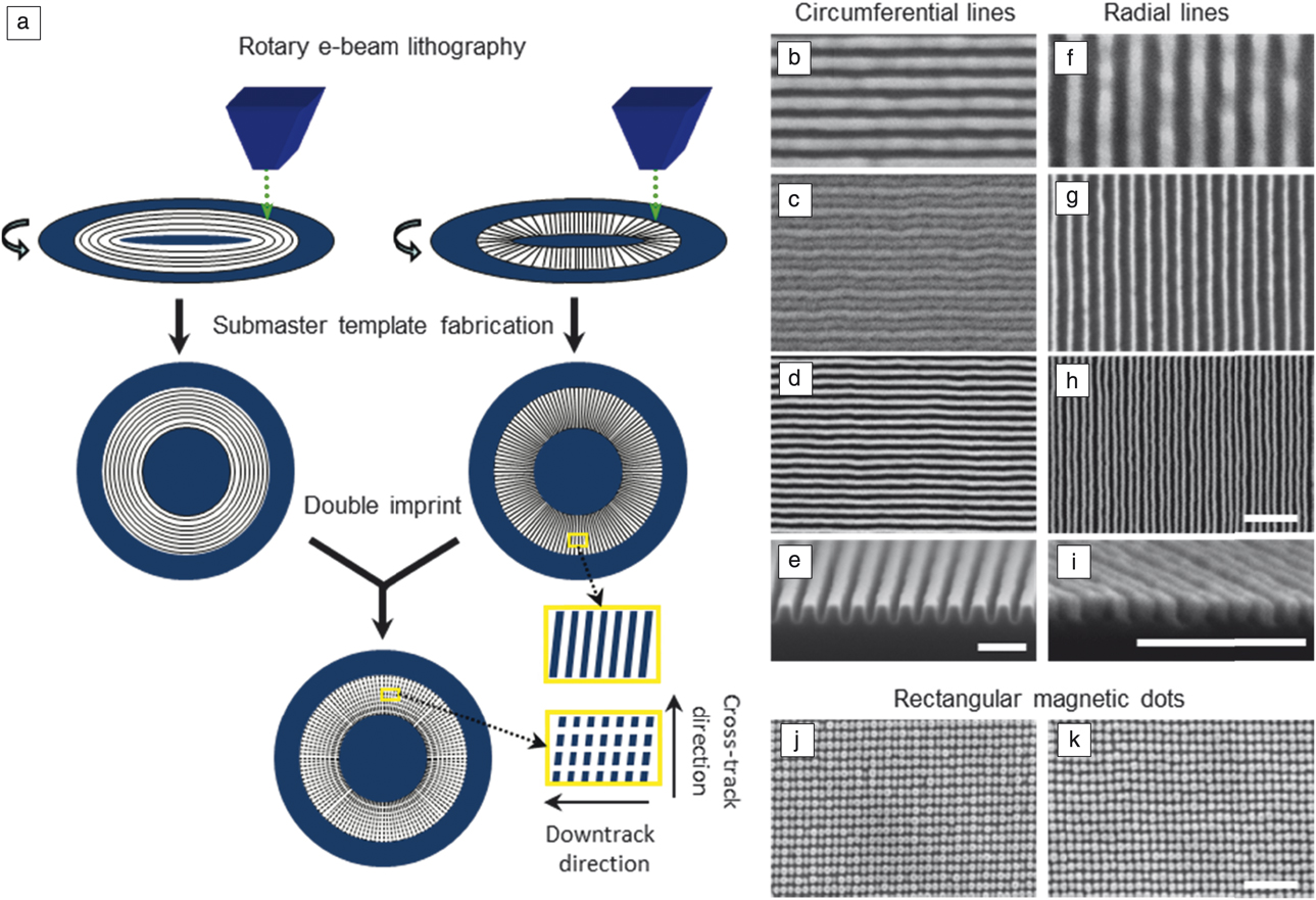
While round bits arranged in a hexagonal lattice maximize areal density for a given critical dimension, rectangular or elongated bits on a rectangular lattice offer advantages for integration in hard-disk drive technology.Reference Albrecht, Arora, Ayanoor-Vitikkate, Beaujour, Bedau, Berman, Bogdanov, Chapuis, Cushen, Dobisz, Doerk, Gao, Grobis, Gurney, Hanson, Hellwig, Hirano, Jubert, Kercher, Lille, Liu, Mate, Obukhov, Patel, Rubin, Ruiz, Schabes, Wan, Weller, Wu and Yang32 Since block copolymers do not naturally assemble into rectangular patterns, a solution has been proposed in which two independent and orthogonal sets of line/space patterns are intersected to form rectangular bits on a rectangular lattice.Reference Ruiz, Dobisz and Albrecht33,Reference Wan, Ruiz, Gao, Patel, Lille, Zeltzer, Dobisz, Bogdanov, Nealey and Albrecht34 Figure 5a illustrates the concept in which two separate nanoimprint templates are fabricated using e-beam and block copolymer lithography. Because of the circular geometry of hard-disk drives, one template is made of generally circumferential lines with some servo features; the second template contains generally zoned and skewed radial lines.Reference Lille, Ruiz, Wan, Gao, Dhanda, Zeltzer, Arnoldussen, Patel, Tang, Kercher and Albrecht35,Reference Wan, Ruiz, Gao, Patel, Albrecht, Yin, Kim, Cao and Lin36 Patterns from the two templates are imprinted and intersected on a third, master template, forming the desired rectangular bits on circumferential tracks. This strategy has demonstrated magnetic recording media with areal densities in the range of 1.0–1.6 Tbpsi as illustrated in Figure 5j–k.
(a) Fabrication of submaster templates from e-beam and block copolymer lithography. One template contains circumferential track lines (left), while the second template includes zoned and skewed radial lines (right). After double imprint on a master template, the two patterns intersect forming rectangular islands. Circumferential lines—top-down scanning electron microscope (SEM) images of (b) e-beam resist pattern with a full pitch, LS = 49 nm; (c) guided PS-b-PMMA pattern with a period, L0 = 24.5 nm; (d) Si lines after pattern transfer. Radial lines—top-down SEM images of (f) e-beam resist pattern with LS = 58 nm; (g) alumina lines formed through sequential infiltration synthesis on guided PS-b-PMMA lamellae with L0 = 29 nm; (h) TiO2 spacer lines with full pitch of 14.5 nm formed through self-aligned double patterning. (e, i) Cross-sectional SEM images of a sister sample as shown in (d, h). (j, k) Top-down SEM images of magnetic dots with areal density of 1.4 and 1.6 Tbpsi. Scale bars = 100 nm.Reference Ruiz, Dobisz and Albrecht33,Reference Wan, Ruiz, Gao, Patel, Lille, Zeltzer, Dobisz, Bogdanov, Nealey and Albrecht34

A rectangular lattice with areal density above 1.2 Tbpsi and bit aspect ratio (BAR) >1.2 necessarily implies that the down-track (radial) full pitch be smaller than 22 nm. Unfortunately, 22-nm pitch seems to be near the limit at which polystyrene-block-poly(methyl methacrylate) (PS-b-PMMA) can sustain both sharp image formation and a robust pattern transfer.Reference Wan, Ruiz, Gao, Patel, Albrecht, Yin, Kim, Cao and Lin36 Therefore, reaching below 22 nm requires either an additional double-patterning step or a different block copolymer altogether. The first demonstrations of rectangular arrays of magnetic islands were performed using self-aligned double patterning (SADP) on top of a PS-b-PMMA defined pattern.Reference Doerk, Gao, Wan, Lille, Patel, Chapuis, Ruiz and Albrecht37,Reference Albrecht, Bedau, Dobisz, He, Grobis, Hellwig, Kercher, Lille, Marinero, Patel, Ruiz, Schabes, Lei, Weller and Tsai-Wei38 Figure 5b–i shows the process used to fabricate submaster templates of circumferential or radial lines. Sparse patterns were first exposed by a rotary stage e-beam, which were used to guide the assembly of PS-b-PMMA thin films. A submaster template forming circumferential lines was fabricated by transferring the block copolymer (BCP) pattern onto the Si substrate.Reference Wan, Ruiz, Gao, Patel, Albrecht, Yin, Kim, Cao and Lin36 For the denser radial lines, an additional SADP process was needed. After directed self-assembly, the PS-b-PMMA pattern was transferred to a mandrel layer through a sequential infiltration synthesis process for smaller critical dimension and smoothness. A spacer layer was conformally deposited using atomic layer deposition. After spacer etch back and mandrel removal, radial lines with halved pitch were obtained.Reference Albrecht, Arora, Ayanoor-Vitikkate, Beaujour, Bedau, Berman, Bogdanov, Chapuis, Cushen, Dobisz, Doerk, Gao, Grobis, Gurney, Hanson, Hellwig, Hirano, Jubert, Kercher, Lille, Liu, Mate, Obukhov, Patel, Rubin, Ruiz, Schabes, Wan, Weller, Wu and Yang32
Meaningful areal densities for a potential HDMR application would likely be above 4 Tbpsi, which will push the lithographic dimensions well below 15-nm full pitch. While SADP and quadruple patterning have evolved as robust patterning techniques in the semiconductor industry and have been used in first media demonstrations, their implementation adds significant complexity and cost. Block copolymers with higher Flory–Huggins interaction parameter (χ),Reference Xiong, Wan, Ishida, Chapuis, Craig, Ruiz and Nealey39,Reference Lane, Yang, Maher, Blachut, Asano, Someya, Mallavarapu, Sirard, Ellison and Willson40 if developed with a concurrent robust pattern transfer strategy, may provide a simpler, more efficient solution to the HDMR scaling challenge to reach 10 Tbpsi.
Concluding remarks
Although significant progress has been made, many challenges remain to satisfy the material requirements for HAMR and HDMR media. Recent technology demonstrations indicate HAMR is well positioned for a full product introduction, with current predictions by industry experts ranging from 2018 to 2020. Based on fundamental magnetic properties of the materials for the recording layer and currently known near-field optical transducers, an extension to around 4–5 Tbpsi seems feasible. To extend magnetic storage technologies to its ultimate limits, HDMR is being developed to enable 10 Tbpsi and beyond.

Kazuhiro Hono is a National Institute for Materials Science (NIMS) Fellow and the director of the Research Center for Magnetic and Spintronic Materials at NIMS, Japan. He is also a professor of materials science and engineering at the University of Tsukuba, Japan. He received his BS and MS degrees in materials science from Tohoku University, Japan, and his PhD degree in materials science and engineering from The Pennsylvania State University in 1988. After completing postdoctoral research at Carnegie Mellon University, and as a research associate at the Institute for Materials Research, Tohoku University, he moved to NIMS as a staff scientist in 1995. His research interests include microstructure–property relationships of metallic materials, in particular, magnetic and spintronic materials and their devices. Hono can be reached by email at kazuhiro.hono@nims.go.jp.

Yukiko K. Takahashi became group leader of the Magnetic Recording Materials Group at the National Institute for Materials Science (NIMS), Japan, in 2016. She received her PhD degree from Tohoku University in 2001. After completing postdoctoral research at NIMS, she became a researcher at NIMS in 2005. Her interests include magnetic materials for device application and magneto-optics. Takahashi can be reached by email at Takahashi.Yukiko@nims.go.jp.

Ganping Ju is a managing technologist (senior director) at the Recording Media Research Center, Seagate Technology. He received his BA degree in physics (1994) from Peking University, China, and MS degree (1995) and PhD degree (1999), both in physics, from Brown University. He joined Seagate Research in 1994 and worked as research staff member, research engineering manager, and director, and led a team in developing and characterizing perpendicular and heat-assisted magnetic recording (HAMR) media. He moved to the Seagate Recording Media Research Center in 2009. His research interests include recording physics, advanced characterization, spin dynamics, magnetic modeling, and understanding key media physics enabling higher areal density recording. His current research focuses on perpendicular media extension and HAMR technology production. Ju can be reached by email at ganping.a.ju@seagate.com.

Jan-Ulrich Thiele joined Seagate Technology in 2008 as a managing technologist (senior director) for media R&D. He currently leads a team of scientists and engineers developing heat-assisted magnetic recording (HAMR) media technology. Significant milestones of this program include the first 1 Tbpsi recording demonstration in 2012, and the demonstration of a fully functioning HAMR drive lasting for 1000 hours of continuous writing in 2014. He received his MSc degree in physics from the University of Hannover, Germany, and his PhD degree in physics from the University of Basel, Switzerland. He was awarded a Feodor-Lynen-Fellowship by the Alexander von Humboldt Foundation in 1996. He has also worked at the IBM Almaden Research Center as a postdoctoral researcher. Thiele can be reached by email at jan-ulrich.thiele@seagate.com.

Antony Ajan is a senior technologist in the magnetic recording media division of Western Digital Corporation. He received his MSc degree in 1993 and PhD degree in 1999 in physics from the Indian Institute of Technology, Bombay, India, in areas related to magnetic thin films and characterization. From 1999 to 2010, he held various research positions at Fujitsu Limited, Japan, developing technologies related to longitudinal, perpendicular, bit-patterned, and heat-assisted media, and on energy-efficient server designs for data center applications. His current research interests include magnetic recording, materials science, and materials characterization. He has published more than 50 articles and patents. Ajan can be reached by email at Antony.Ajan@wdc.com.

XiaoMin Yang is a research manager working on advanced storage technology development at Seagate Research. He received his PhD degree in materials science and engineering from Southeast University, China, in 1994. After completing postdoctoral research at The University of Tokyo, Japan, and as a research scientist at the University of Wisconsin–Madison, he joined Seagate Research as a research staff member in 2001. His research interests include a variety of advanced lithography techniques, including e-beam lithography, nanoimprint lithography, directed self-assembly of block copolymers, and nanofabrication in the sub-20-nm regime. He has 100+ publications and holds 30 US patents. Yang can be reached by email at XiaoMin.Yang@seagate.com.

Ricardo Ruiz is a research technologist at Western Digital Corporation. He received his PhD degree in physics from Vanderbilt University in 2003. From 2013 to 2016, he managed a Nanopatterning and Self-Assembly Group at Hitachi Global Storage Technologies (HGST). He was a research staff member at HGST, where he helped introduce block copolymer lithography for magnetic bit-patterned media technology. He was also a postdoctoral scientist at IBM T.J. Watson Research Center. His current research interests focus on alternative nanofabrication techniques for memory and storage devices, block copolymer lithography, and colloidal self-assembly. He is a Fellow of the American Physical Society and was the recipient of the 2016 ACS Applied Materials and Interfaces Young Investigator Award. Ruiz can be reached by email at ricardo.ruiz@wdc.com.

Lei Wan is a research technologist at Western Digital Corporation. He received his PhD degree in chemical engineering at Wayne State University in 2009. He was an intern engineer at Seagate in 2008. From 2009 to 2011, he was a postdoctoral researcher at the University of Wisconsin–Madison. He then joined the Bit Patterned Media Group at Western Digital. His responsibilities included directed self-assembly of block copolymers, e-beam lithography, and pattern transfer. His current research focuses on nonfabrication and process integration of nonvolatile memory devices. He has published 50 articles and holds 15 patents. Wan can be reached by email at lei.wan@wdc.com.