I. INTRODUCTION
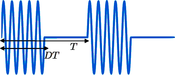
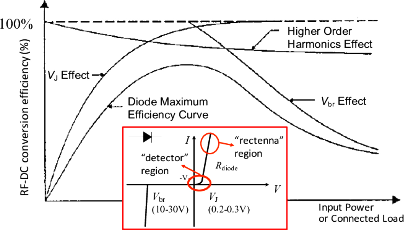
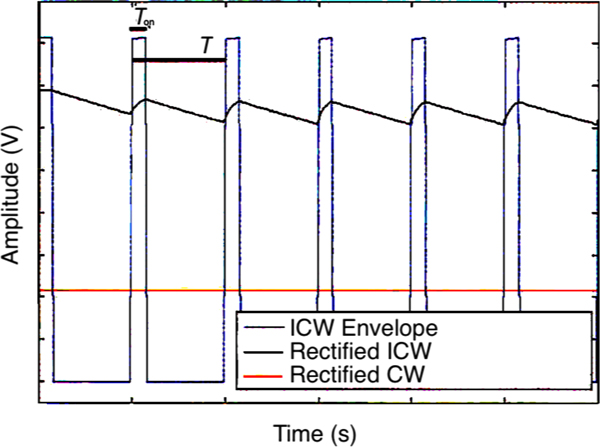
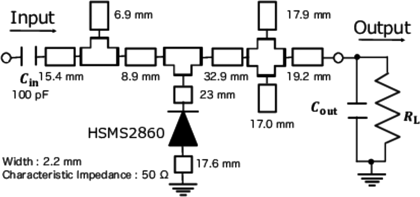
Microwave power transfer (MPT) can provide solutions to some critical problems. Currently, the necessity of the Internet of Things (IoT) technique is increasing. IoT requires a flexible configuration of sensor networks, which is hindered by wired-charging sensors and MPT can be the solution. MPT techniques have been improved [Reference Brown1, Reference Brown2]; however, there are some shortcomings, namely the lack of interference with communication and low transmitting efficiency, which will be the focus of our study. MPT requires rectifiers for the RF-DC conversion. Information and power transmission can be operated at the same frequency using pulse-modulated waves [Reference Shinohara, Georgiadis, Nikoletseas and Yang3]. On the other hand, simultaneous wireless information and power transmission using pulse modulation has been considered in some research [Reference Claessens, Schreurs and Pollin4, Reference Claessens, Pan, Rajabi, Schreurs and Pollin5]. Since pulse-modulated waves are compatible with the MPT system of communication, we have used it herein (Fig. 1) [Reference Matsumoto and Takei6]. The modeling, simulation, and analytical calculation methods have been discussed previously [Reference Nahas7–Reference Guo, Zhang and Zhu9]. In addition, the general characteristics of rectifiers have been studied [Reference McSpadden, Fan and Chang10, Reference Yoo and Chang11]. Figure 2 shows the general characteristics of the RF-DC conversion efficiency [Reference Yoo and Chang11]. The use of signals with a high peak-to-average power ratio (PAPR) improves the RF-DC conversion efficiency [Reference Boaventura, Belo, Fernandes, Collado, Georgiadis and Carvalho12]. The efficiency decreases with a low input voltage, and a small voltage applied to the diode is adversely affected by the threshold voltage (Fig. 2). In contrast, with a high input, the voltage applied to the diode exceeds the breakdown voltage, and the RF-DC conversion efficiency decreases. Herein, the RF-DC conversion efficiency is improved using the low input voltage. Figure 3 shows the comparison between the output voltage under continuous wave (CW) and intermittent CW (ICW) inputs displaying the increasing voltage of rectifiers under the input with a high PAPR. The application of chaotic waves [Reference Collado and Georgiadis13], ultra-wide bandwidth signals [Reference Lo, Yang, Tsai, Lee and Yang14], multisine waves [Reference Carvalho, Remley, Schreurs and Card15], or modulated waves [Reference Collado and Georgiadis16] can improve the RF-DC conversion efficiency because these waves have a high PAPR, similar to the pulse-modulated waves. Thus, pulse modulation is effective at improving the RF-DC conversion efficiency of rectifiers and solving other problems. Some studies are focusing on a pulse-modulated wave as we mentioned above [Reference Claessens, Schreurs and Pollin4, Reference Claessens, Pan, Rajabi, Schreurs and Pollin5]. These research papers focused on information transmission by amplitude shift keying and discussed about the output voltage wave for simultaneous wireless information and power transmission (SWIPT). Their research shows pulse modulation is at least effective for SWIPT. This research discusses operation in more detail and focuses on improving RF-DC conversion efficiency of rectifiers. A pulse-modulated wave has two fundamental frequencies, repetition and carrier frequencies. The harmonic balance method is of no use for analyzing the operation under pulse-modulated waves. To analyze the operation of the rectifiers under pulse-modulated waves, one needs to employ the transient method since the analysis using the harmonic balance method is difficult. In this study, the operation of single-shunt rectifiers (Fig. 4) under pulse-modulated input is studied. The operation of rectifiers with pulse-modulated input was discussed previously [Reference Ibrahim17]. However, this work did not discuss thoroughly enough the details regarding the circuit design method and the conditions for using pulse-modulated waves. We focus on the effects of smoothing capacitance and of the parameters of the pulse modulations in this research. In addition, the effectiveness of pulse modulation for improvement and rectifier operations is discussed in detail. Our study analyzes a general operation of rectifiers with pulse-modulated waves and shows the effectiveness of the pulse modulation for improving the RF-DC conversion efficiency by theory, simulations, and experiments. In addition, we suggest an analytical approach for rectifiers to design pulse-modulated waves which have low repetition frequency.
Waveform of pulse-modulated waves.

Theoretical characteristics of the RF-DC conversion efficiency [Reference Brown2].

Comparison between the output voltage using the CW and ICW inputs [Reference Boaventura, Belo, Fernandes, Collado, Georgiadis and Carvalho12].

Schematic of single-shunt rectifiers.

II. THEORETICAL ANALYSIS OF THE RECTIFIER OPERATION UNDER PULSE-MODULATED INPUT
A pulse-modulated wave rectifier that utilizes the charging and discharging of a smoothing capacitor significantly impacts V out. This section discusses the operation of rectifiers as affected by a smoothing capacitor and considers the operation of the rectifiers under pulse modulation.
A) Parameters used in this paper
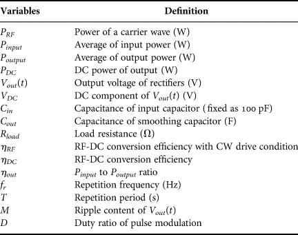
Table 1 shows the definition of the variables used herein. The following equations are used to express the relations among these variables:
 $$P_{input} = DP_{RF}$$
 $$P_{output} = \displaystyle{1 \over T}\int_0^T {\displaystyle{{V_{out}{(t)}^2} \over {R_{load}}}dt} $$
 $$P_{DC} = \displaystyle{{V_{DC}^2} \over {R_{load}}}$$
 $$V_{DC} = \displaystyle{1 \over T}\int_0^T {V_{out}\lpar t \rpar dt} $$
 $$\eta _{DC} = \displaystyle{{P_{DC}} \over {P_{input}}}$$
 $$\eta _{out} = \displaystyle{{P_{output}} \over {P_{input}}}$$
 $$M = \displaystyle{{{\rm max}\,{\rm (}V_{out}{\rm (}t{\rm ))}-{\rm min}\,{\rm (}V_{out}{\rm (}t{\rm ))}} \over {V_{DC}}}$$
Definition of variables.

B) Discussion on the fluctuation of V out
The fluctuation of V out is caused by the charging and discharging of the smoothing capacitor. The amount of electric charge stored during charging is designated as Q. In the steady state, the amount of electrical charge stored during the charging period is same as that flowing out from C out during the discharging period. Hence, equation (8) is obtained:
 $${\eqalign{Q & = C_{out}(V_{out}(t_0 + DT)-V_{out}(t_0))\quad \cr & = \int_{t_0 + DT}^{t_0 + T} {\displaystyle{{V_{out}(t)} \over {R_L}}} dt.}} $$
In contrast, equation (9) is obtained:
 $$\int_{t_0 + DT}^{t_0 + T} {\displaystyle{{V_{out}(t)} \over {R_L}}dt \le \displaystyle{{{\rm max\;} (V_{out})} \over {R_L}}(1-D)T.} $$
Therefore, the maximum value of the voltage change is expressed using equation (10):
 $$\max (V_{out})-\min {\rm (}V_{out}{\rm )} \le \displaystyle{{{\rm max}(V_{out})} \over {C_{out}R_L}}(1-D)T.$$
Equation (11) is derived from equation (10):
 $$\displaystyle{{{\rm min(}V_{out}{\rm )}} \over {{\rm max}(V_{out})}} \ge 1-\displaystyle{{(1-D)T} \over {C_{out}R_L}}.$$
Consequently, equation (12) is derived as a condition wherein a sufficiently small fluctuation occurs:
 $$C_{out}\gg \displaystyle{{1-D} \over {R_Lf_r}}.$$
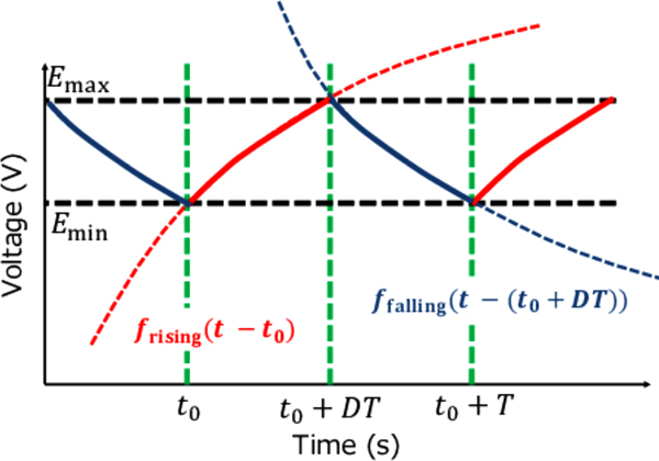
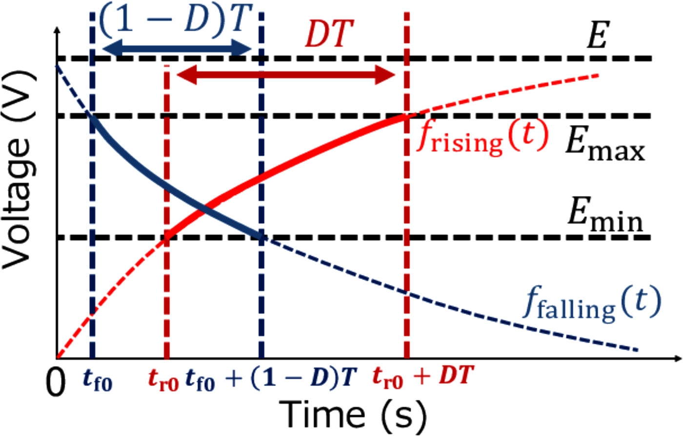
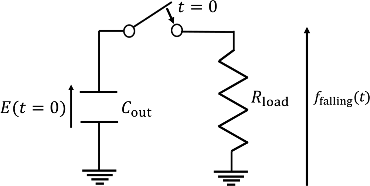
The operation of rectifiers with the condition satisfying equation (12) is discussed in the next subsection. With the condition equation (12) unsatisfied, the output voltage wave is in the steady state, as shown in Fig. 5. The waveform consists of two functions, f rising and f falling. Figure 6 shows the forms of their functions. E means the DC voltage in the steady state with CW input, which has P RF input power. E max and E min respectively indicate the maximum and minimum voltages of an output wave under pulse-modulated input. Herein, the change in V out during charging is denoted as f rising(t) and that during discharging as f falling(t). f rising(t) and f falling(t) satisfy equations (13) and (14), respectively:
 $$\eqalign{& f_{rising}(DT + t_{r0})-f_{rising}(t_{r0}) \cr & \quad = f_{falling}((1-D)T + t_{f0})-f_{falling}(t_{f0}),} $$
 $$f_{falling}(t_{f0}) = f_{rising}(DT + t_{r0}).$$
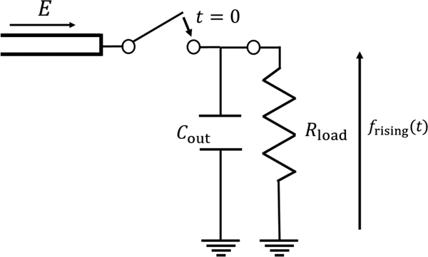
These are the boundary conditions of a steady state. When we know the transient operations of rectifiers during charging and discharging, the operations of rectifiers under the pulse-modulated waves can be calculated by equations (13) and (14). Figures 7 and 8 show the equivalent circuits at the rising and falling edges. f rising(t) and f falling(t) can be determined by the easy calculations shown below:
 $$f_{rising}(t) = E\left( {1-\exp {\rm \;} \left( {-\displaystyle{t \over {\tau_{rising}}}} \right)} \right),$$
 $$f_{falling}(t) = E\exp {\rm \;} \left( {-\displaystyle{t \over {\tau_{falling}}}} \right).$$
V out with pulse-modulated waves in the steady state.

Definition of f rising(t) and f falling(t).

Equivalent circuit at the rising edge.

Equivalent circuit at the falling edge.

When the C in and junction capacitance of the diode are small, τ falling is equal to C outR load. In addition, equation (16) has been discussed and used in some papers [Reference Claessens, Schreurs and Pollin4, Reference Claessens, Pan, Rajabi, Schreurs and Pollin5]. The rise operation is complex for the microwave propagation; therefore, τ rise cannot be obtained from a theoretical analysis.
C) Analysis of the rectifier with a sufficiently large smoothing capacitor
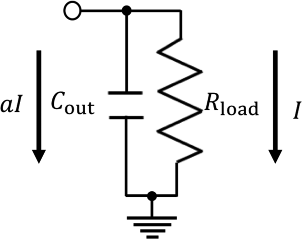
This subsection discusses the rectifier operation under the conditions of equation (12). The current is defined as shown in Fig. 9. We let the average of I and V out be represented as  $\bar{I}$ and
 $\overline {V_{out}} $. In addition, the average current flowing through the capacitor during charging is a times as large as
 $\bar{I}$. When the fluctuation of V out is sufficiently small, the fluctuation of I is also very small. Equation (17) is obtained by considering the conservation of charge during the charging and discharging of a steady state capacitor:
 $$a\bar{I}D = (1-D)\bar{I}.$$
Rectifier load.

With a sufficiently small voltage fluctuation, the apparent impedance also has a sufficiently small change. Let R be the resistance observed from the rectifier circuit during charging as expressed in equation (18):
 $$R = \displaystyle{{\overline {V_{out}}} \over {(a + 1)\bar{I}}}.$$
R load is represented by equation (19):
 $$R_{load} = \displaystyle{{\overline {V_{out}}} \over {\bar{I}}}.$$
Equation (20) is derived using equations (17)–(19):
 $$R = DR_{load}.$$
Equation (20) shows that the rectifier operates under the conditions of input power P input and load resistance DR L during charging. Using η RF with P input of input power and DR L of load resistance, we obtain equation (21):
 $$\overline {V_{out}} = \sqrt {\displaystyle{{\eta _{RF}P_{input}R} \over D}} = \sqrt {\eta _{RF}P_{input}R_{load}}. $$
Equation (22) is derived from equation (21):
 $$P_{DC} = \displaystyle{{{\overline {V_{out}}} ^2} \over {R_{load}}} = \eta _{RF}P_{input}.$$
Equation (23) follows from the above equations:
 $$\eta _{DC} = \eta _{RF}.$$
Equation (23) shows that the RF-DC conversion efficiency with CW having P input/D can be obtained. In addition, equation (20) states that the optimum load of this condition becomes 1/D times that under the CW drive conditions. These equations are obtained with satisfied conditions of equation (12) and our theory is not related to the matching network and the value of R load. Therefore, these equations are generally obtained when using pulse-modulated input and equation (12) is satisfied. Therefore, the optimum matching network is same as CW input rectifiers with DR load.
III. BASIC ANALYSIS OF RF-DC CONVERSION WITH PULSE MODULATION
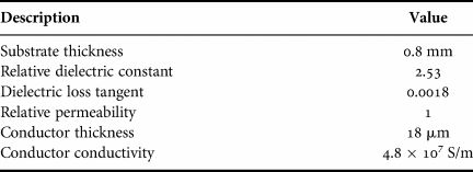
The rectifier with CW, which has 10 mW of input power and a 2.45 GHz frequency drive, is designed using the harmonic balance simulation. The parameters shown in Table 2 are used for the board parameter setting. Figure 4 presents a schematic of the designed single-shunt rectifier.
Board parameters of microstrip substrate in the simulations.

A) Estimation of the rectifier operation
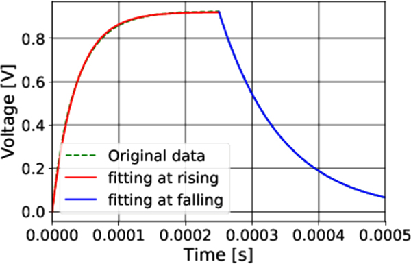
The pulse-modulated waves have two basic frequencies: repetition and carrier frequencies. This study exploits the carrier frequency of 2.45 GHz and the repetition frequency is below 1 MHz. Thus, the pulse-modulated waves possess excessive frequency components. In this case, the rectifier operation cannot be analyzed using the harmonic balance method. Therefore, only the transient simulation is useful for analyzing the operation of rectifiers with the pulse-modulated input. However, for the transient analysis, the transient simulation requires the time step to be sufficiently small compared to the period of the carrier wave. Hence, analyzing the operation of the rectifiers by taking into account only one condition is time consuming. For this reason, the output voltage waveform is estimated using equations (13) and (14) using f rising(t) and f falling(t). The exponential function approximates the output voltage wave. It is estimated that f rising(t) and f falling(t) can be expressed by equations (15) and (16), respectively. Then, the simulation result should confirm consistency of this assumption. The output voltage of the rectifiers with a single-shot CW input is simulated. The chosen simulation parameters are the input duration, the average power, and the frequency being equal to 250 µs, 1 mW, and 2.45 GHz, respectively; R load and C out are 2 kΩ and 47 nF, respectively. The green line in Fig. 10 shows the simulation result of the transient. Equations (15) and (16) fit the green line using the Levenberg–Marquardt method [Reference Moré18]. The red and blue lines in Fig. 10 show the fitting result of equations (15) and (16), respectively. Figure 10 exhibits a complete match of the green, red, and blue lines. Therefore, the former estimation is quite correct. The application of the fitting procedure allows us to deduce the value of τ rising as 3.576 × 10⁻⁵ and that of τ falling as 9.408 × 10⁻⁵. In this case, the rise and fall times become 78.6 and 206.7 µs, respectively.
Simulated V out using transient analysis.

B) Estimated and simulation characteristics of the rectifiers
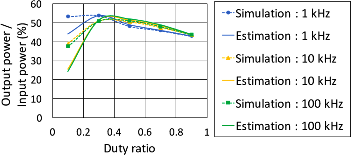
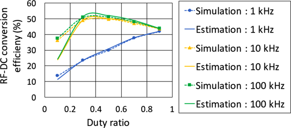
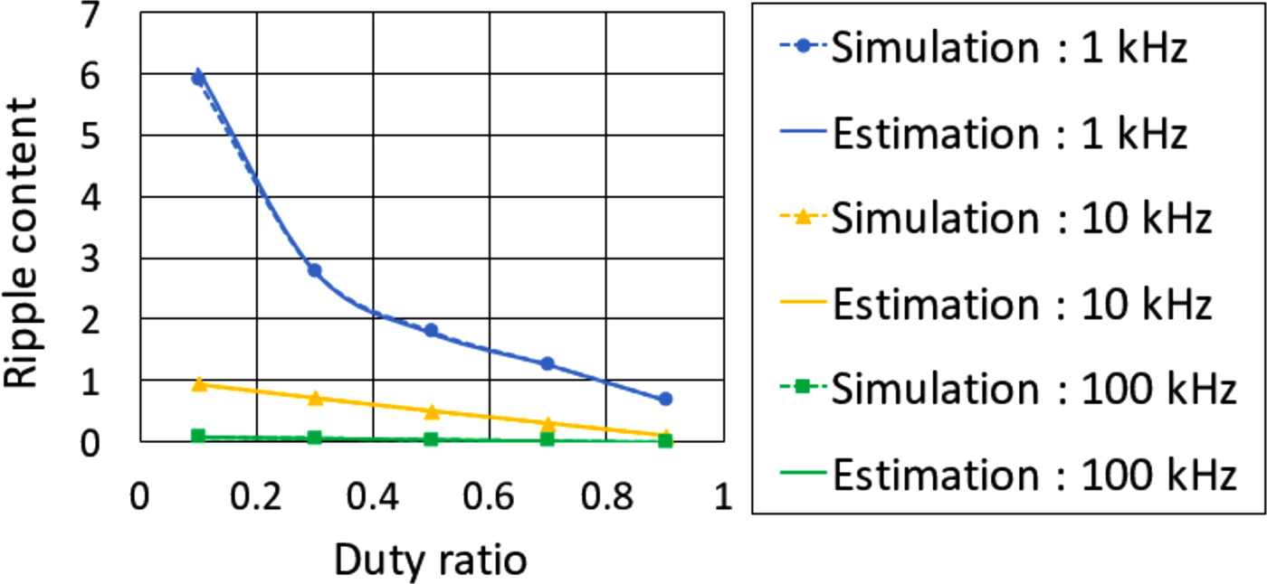
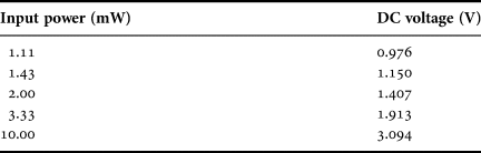
In this subsection, the output voltage is estimated in a steady state using the values of τ rising and τ falling in subsection A). Using this estimation, the V out values in various conditions derived using numerical calculations are known as long as the load components are fixed. Since numerical calculations are quick, the time for analyzing the operation of rectifiers under the pulse-modulated input is reduced. If the value of E is known, the performances of rectifiers can be calculated by equations (13) and (14) using numerical analysis. E is equal to the output voltage of the rectifiers with a CW input black, which has the same power as a career wave (P RF). Thus, E is calculated using the harmonic balance or transient simulations. Table 3 shows the simulated DC voltage in a steady state with the condition that the values of R load and C out are 2 kΩ and 47 nF, respectively. Using the data in Table 3, η DC, η out, and M are calculated at P input of 1 mW. Figures 11, 12, and 13 show η out, η DC, and M, respectively; they demonstrate a good agreement between the estimation and simulation results. But with D = 0.1, Figs 11 and 12 show differences and Fig. 13 shows a complete match. These results indicate that our proposed method is not good for estimating η out and η DC under a condition in which the output voltage has little fluctuation and D is also little. When D is very small, the error of the rising waveform will affect the calculation results. Figures 11 and 12 show an error of 20%. This large error can occur from only a few percent errors in the rising waveform. In addition, the transient simulation can easily generate a numerical error with small D. Therefore, the simulation and our proposed estimation method are not good for analyzing the steady state with too small D. Hence, when D is not so small and f r is less than or equal to 100 kHz, the estimation method mentioned in subsection A) is consistent with the simulation of rectifiers under a pulse-modulated wave input.
Simulated and estimated η out depending on f r and D.

Simulated and estimated η DC depending on f r and D.

Simulated and estimated M depending on f r and D.

Simulated DC voltage in the steady state.

C) Experimental characteristics of rectifiers
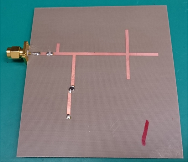
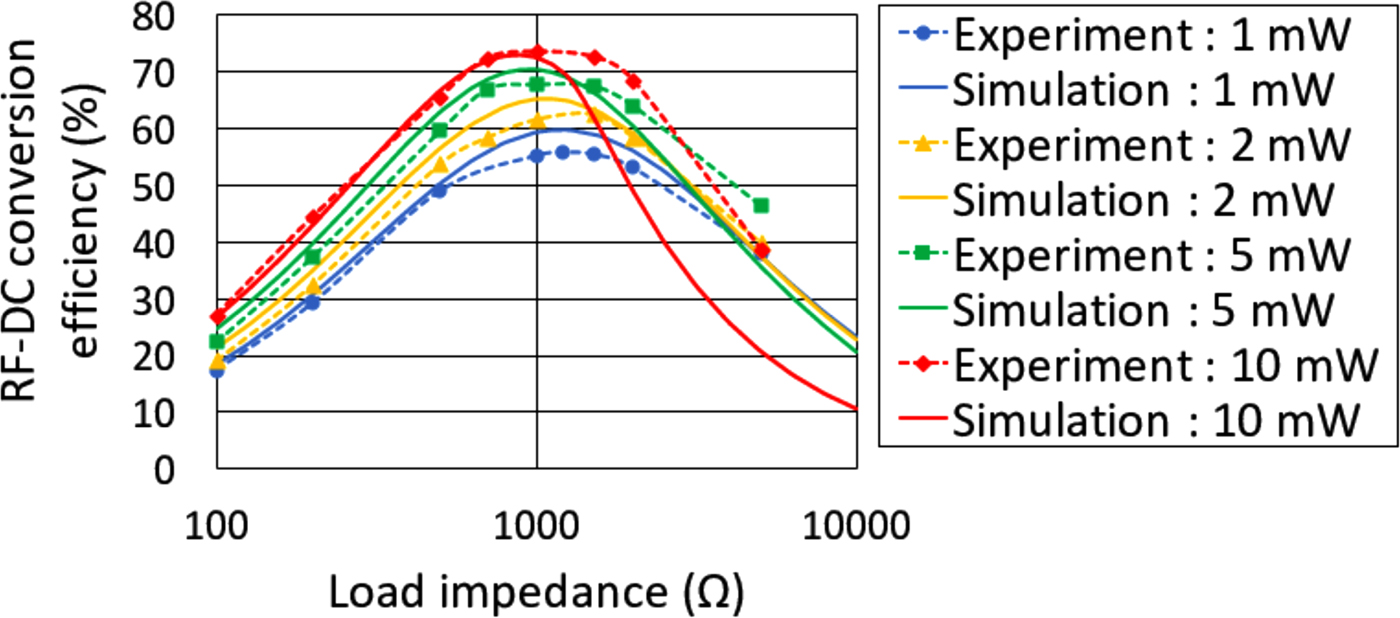
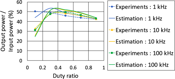
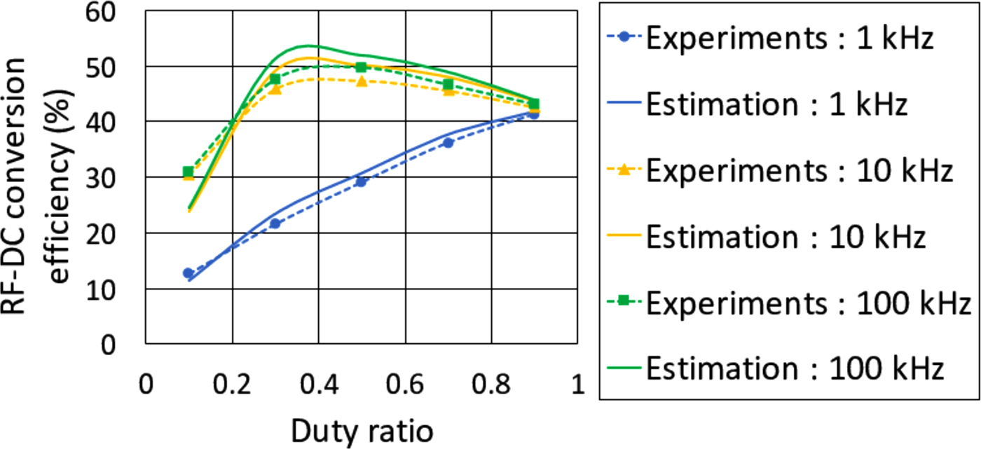
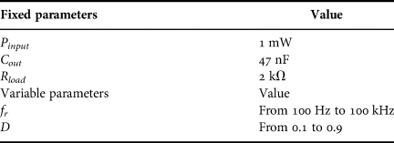
Figure 14 presents a rectifier fabricated using the parameters in Fig. 4. Figure 15 shows the change of η DC with CW depending on P input and R load. In the experiments and simulations, C in and C out are set as 100 pF and 47 nF, respectively. The results of the experiments and simulations show similar tendencies. The rectifier experiments used the conditions shown in Table 4. Figures 16, 17, and 18 exemplify the experimental and estimation results indicating a good agreement. But, with D = 0.1, Figs 16 and 17 show around 10% errors. Also the experimented and simulated values (Figs. 11 and 12) have around 10% errors. These errors occur by the reasons mentioned in the previous section. Figure 16 reveals that η out increases with the decrease of f r at low D. When f r is high, equation (12) is satisfied. In this case, the observed load resistance of rectifiers becomes 1/D times R load because of equation (20). Letting the apparent resistance R eq = R/D, the rectifiers operate with P RF of input power and R eq of load resistance. Figure 15 shows that a 20 kΩ load resistance is much higher than the optimum resistance, and the RF-DC conversion efficiency is very low under such conditions. In contrast, if equation (12) is not satisfied, and the output voltage wave becomes a pulse wave with a low f r, the rectifier operates with P input/D and 2 kΩ of input power and load resistance, respectively. A 2 kΩ load impedance is around the optimum value with from 1 to 10 mW input. Therefore, the lower D is, the more η output become.
An experimented rectifier.

The change of η DC with CW input depending on P input and R load.

Experimental and estimated η out depending on f r and D.

Experimental and estimated η DC depending on f r and D.

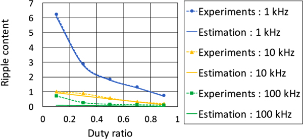
Experimental and estimated M depending on f r and D.

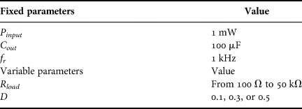
Parameters in the experiments in Section III subsection C).

Figure 17 shows the increase in the experimental η DC and the simulated η DC depending on f r. η DC is proportional to D with a low f r, when equation (12) is not satisfied, and the output voltage becomes a pulse wave. Equation (24) in this case provides the relation between η DC and η out:
 $$\eta _{DC} = D\eta _{out}.$$
Thus, η DC is proportional to D, consistent with the results in Fig. 17. On the other hand, Fig. 17 shows the peak around D = 0.4 with f r is 10 or 100 kHz. In these cases, f r is sufficiently high and the output voltage has little fluctuation. The apparent power and impedance are P input/D and DR L, respectively. Figure 15 shows the optimum impedance of our experimented rectifier was more than ~1 kΩ when the input power was lower than or equal to 10 mW. In this paper, D is larger than or equal to 0.1. Therefore, as D becomes smaller, the apparent input power further closer to the optimum power and the apparent resistance becomes further away from the optimum impedance. For this trade-off relationship between the apparent power and impedance, our experimented rectifier had the optimum value of D around 0.4.
Figure 18 shows the monotonic decrease of M depending on the increase of f r and D. V DC increases depending on D and max (V out) − min (V out) decreases depending on f r, which explains the decrease of M in Fig. 18.
IV IMPROVEMENT OF RF-DC CONVERSION WITH PULSE MODULATION
Although simulations of the rectifiers under the pulse-modulated input are time-consuming, particularly if C out is very large, V out can be quickly obtained in the experiments. In this section, the operation of the rectifiers is experimentally analyzed in detail, and the results are compared in light of the theoretical discussion that was presented in Section II.
A) Influences of C out on the rectifier operation
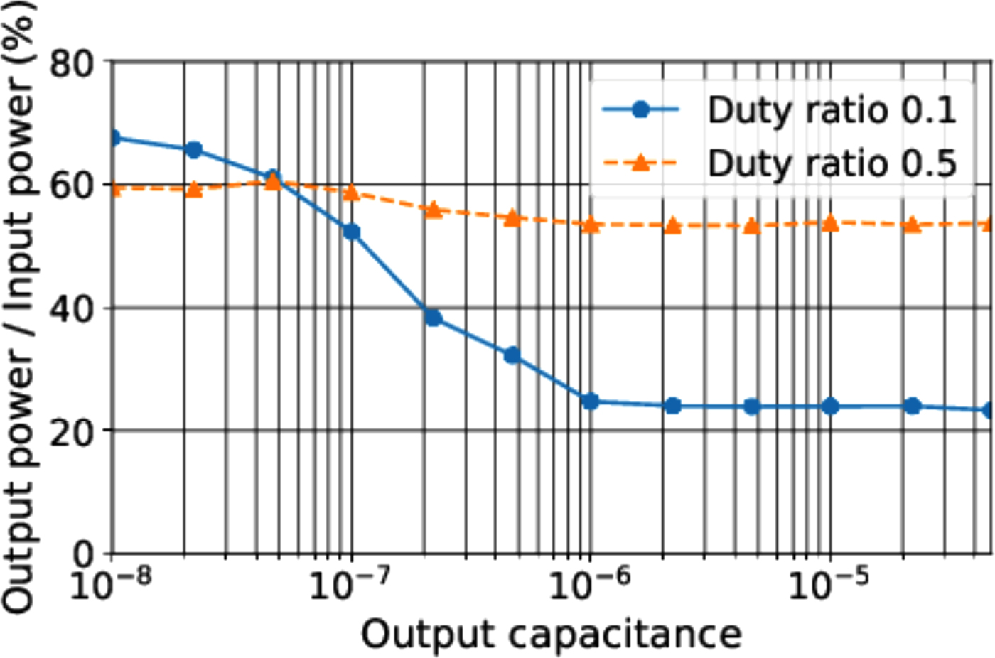
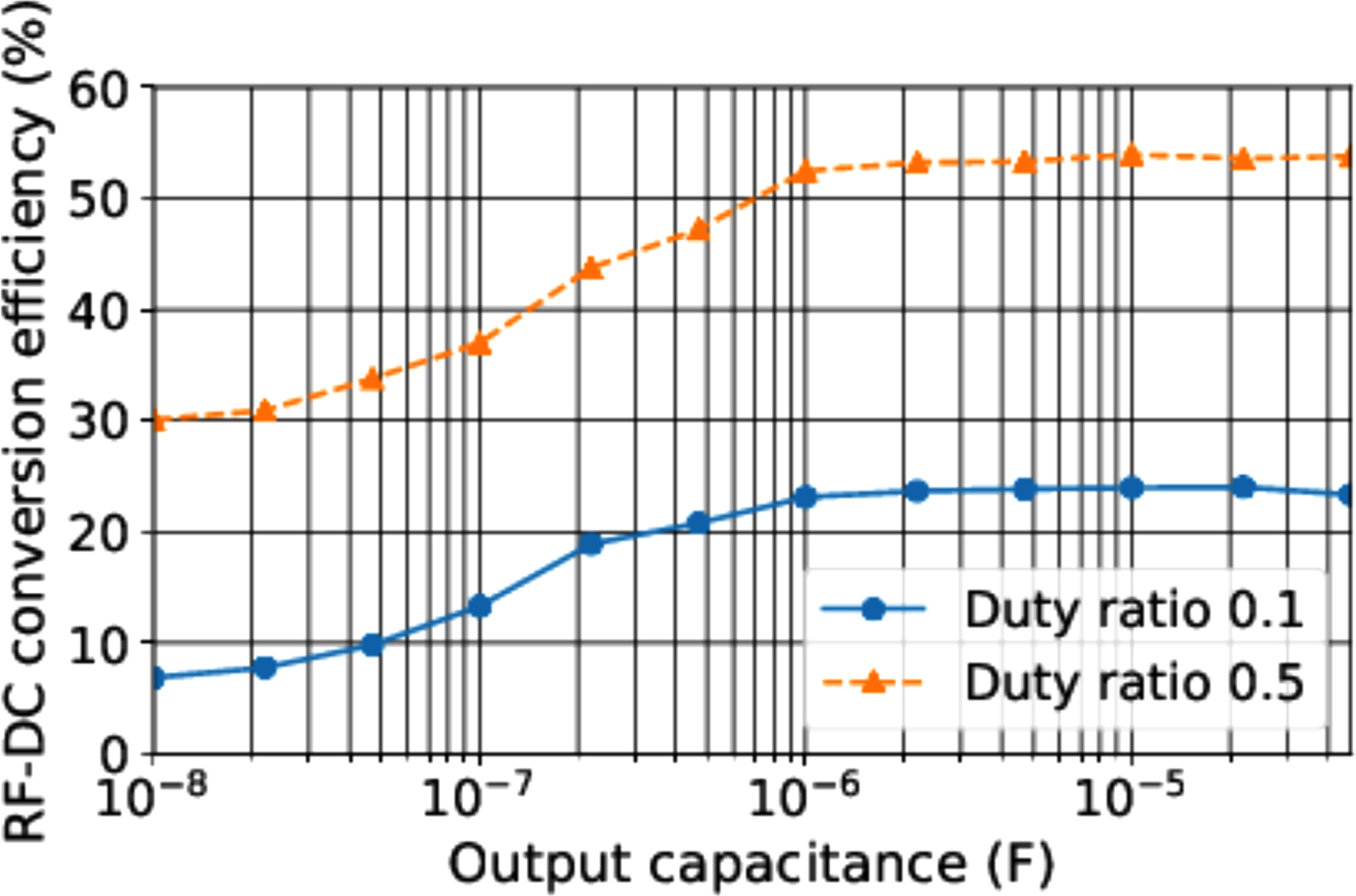
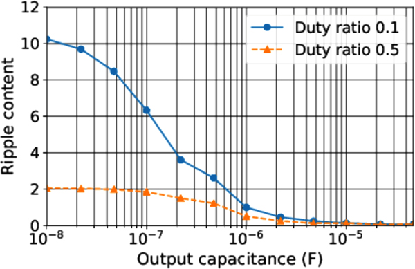
In this subsection, the validity of the condition expressed in equation (12) is examined. The parameter settings and conditions from Table 5 are used in the experiments with the outcome presented in Figs. 19, 20, and 21. In this case, C out ≫ (1 − D) × 10−6 is necessary for satisfying equation (12). Large changes occur at around C out when it is equal to (1 − D) × 10−6 as shown in Figs. 19, 20, and 21. This indicates that the condition in equation (12) is consistent with the actual operation of the rectifiers under the pulse-modulated input.
Changes in η out depending on C out and D.

Changes in η DC depending on C out and D.

Changes in M depending on C out and D.

Parameters setting in Section IV subsection A).

When C out is sufficiently small, the output voltage becomes a pulse wave and the rectifier operates with the P RF of input power and R load of load resistance. Also, η DC is expressed by equation (24) and η out is same as that of CW input. From Fig. 15, η out with D = 0.1 and D = 0.5 should be ~70 and 60% respectively, and η DC with D = 0.1 and D = 0.5 should be ~7 and 30%, respectively. This assumption is consistent with Figs 19 and 20. Next, we consider the condition that C out is sufficiently large. η out and η DC should be the same value and equal to the η DC with P RF of input power and R eq of load resistance. This assumption is also consistent with Figs 19 and 20. These results indicate that the rectifier operation is changed by the value of C out. This is the reason for the crossing in Fig. 19. If the application can use the pulse wave, the condition, where equation (12) is not satisfied, is better than satisfying equation (12). Therefore, we should change the conditions depending on applications for improving the RF-DC conversion efficiency. Figures 19 and 20 show that the C out value is useful and important for managing conditions. Even if f r is not so high, large C out satisfies the conditions of equation (12). Therefore, pulse modulation is useful for all applications by managing the C out value.
B) Improvement in η DC with a sufficiently large smoothing capacitor
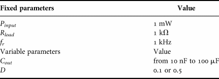
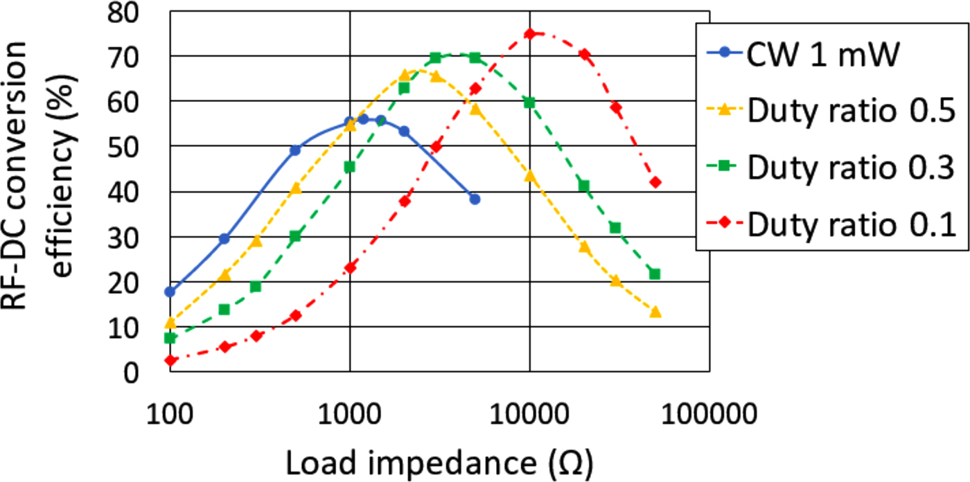
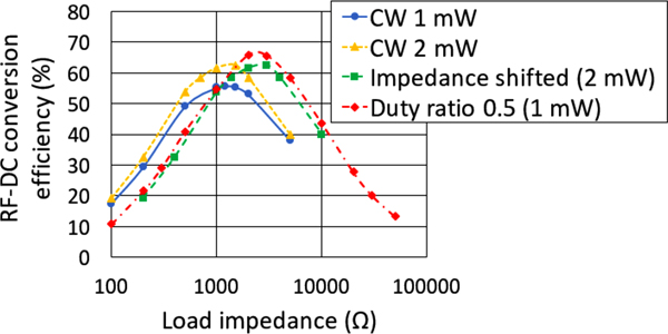
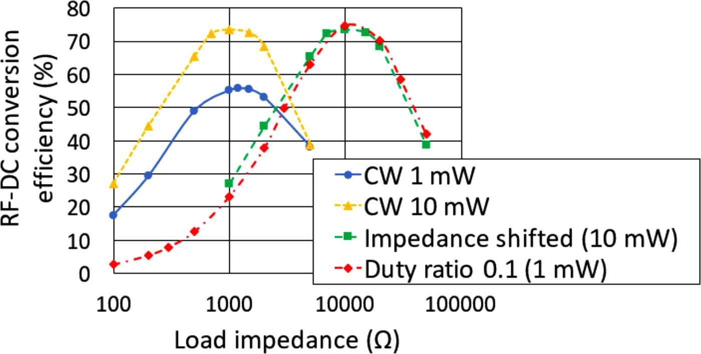
In this subsection, the η DC is discussed depending on the R load, which satisfies the condition of equation (12). The parameters shown in Table 6 are used in the experiments. A 100 µF C out is sufficiently large for satisfying the condition of equation (12), wherein V out is regarded as a constant. Figure 22 reveals the change of η DC depending on R load and D and the increasing maximum η DC at the vanishing D, in accordance with equation (23). Figure 23 shows the comparison between the η DC with the pulse-modulated-input (a duty ratio of 0.5 and an input power of 1 mW) and that with CW input power of 2 mW. The green line indicates the relation of the RF-DC conversion efficiency with the CW, which is 2 mW versus 1/D times R load. Figure 24 shows the comparison between the η DC under the pulse-modulated input (a duty ratio of 0.1 and an input power of 1 mW) and that with CW input of 10 mW input power. The green line indicates the relation of the RF-DC conversion efficiency with the CW, which is 10 mW versus 1/D times R load. The red and green lines match as shown in Figs 23 and 24, respectively. This is consistent with equations (20) and (23) and proves that by using pulse modulation, the RF-DC conversion efficiency with CW, which has P input/D and the optimum resistance shift 1/D times R load, can be obtained. This indicates that the RF-DC conversion efficiency of the rectifiers having a lower input can be improved using pulse modulation.
The change in the η DC depends on the R load with sufficiently large C out.

The comparison between the η DC with pulse-modulated input, which has the duty ratio of 0.5 and the input power of 1 mW, and that with CW input, which has the input power of 2 mW.

The comparison between the η DC with pulse-modulated input, which has the duty ratio of 0.1 and the input power of 1 mW, and that with CW input, which has the input power of 10 mW.

Parameters setting in Section IV subsection B).

V. CONCLUSIONS
In this study, the operation of the rectifiers under the pulse-modulated input has been discussed. The fluctuation of the output voltage wave has to be considered when using the pulse-modulated waves. This paper shows the estimation, simulation, and experimentation of rectifiers under the pulse-modulated input, and all of the results are in good agreement.
A smoothing capacitance C out is quite important for the improvement of RF-DC conversion efficiency that can be attained by using a pulse modulation. When the capacitance is sufficiently small, the output voltage wave is almost a pulse wave and its η DC is not so high. Conversely, with a sufficiently large capacitance, η DC is improved from η RF with P input to η RF with P RF. The necessary condition for the smoothing capacitance value was discussed in Section II subsection B) and is expressed by equation (12). The optimum impedance with equation (12) satisfied was also discussed in Section II subsection C) and that is increased to an inverse of the duty ratio times η RF with P RF input.
We proposed the estimation method of a rectifier operation under a pulse-modulated wave input and the consistency with simulation results was discussed in Section III subsections A) and B). In addition, we compared the estimation and experimental results in Section III subsection C). When D = 0.1, the estimation and simulation results are not matched and the reason seems to be the calculation error. However, at least when D is larger than or equal to 0.3, our proposed method shows good consistency with both simulation and experimental results. In addition, our proposed method takes less time than the transient simulation. Therefore, this method was effective for estimating the rectifier operations with not so high f t.
The experiments regarding the influence of the smoothing capacitor and the effectiveness of a pulse modulation are discussed in Section IV. The condition of equation (12) was consistent with the experimental result. The maximum RF-DC conversion efficiency was improved by using pulse modulation. The characteristics were also consistent with the discussion in Section II. C out value is important and useful for managing the conditions and it decides whether equation (12) is satisfied or not. Therefore, even if f r is not too high, pulse modulation is useful with using a proper smoothing capacitance.
Consequently, we showed the effectiveness of a pulse modulation and succeeded in performing the operational analysis of the rectifiers with a pulse-modulated input.
 Takashi Hirakawa received his B.S. degree in Electrical and Electronic Engineering from Kyoto University in 2016. From 2016, he is studying about microwave techniques in the Electrical Engineering of Kyoto University.
 Ce Wang received his B.S. degree in Integrated System Engineering from the Kyushu Institute of Technology, Fukuoka, Japan, in 2014. He is currently pursuing his M.S. degree in electrical engineering at Kyoto University. His current research interests include low-power rectenna and wireless power transmission system design.
 Naoki Shinohara received his B.E. degree in electronic engineering, M.E. and Ph.D. (Eng.) degrees in electrical engineering from Kyoto University, Japan, in 1991, 1993, and 1996, respectively. He was a research associate in Kyoto University from 1996. From 2010, he has been a professor in Kyoto University. He has been engaged in research on Solar Power Station/Satellite and Microwave Power Transmission system. He is IEEE MTT-S Technical Committee 26 (Wireless Power Transfer and Conversion) vice chair, IEEE MTT-S Kansai Chapter TPC member, IEEE Wireless Power Transfer Conference advisory committee member, executive editor of international journal Wireless Power Transfer (Cambridge Press), technical committee on IEICE Wireless Power Transfer, communications society member, Japan Society of Electromagnetic Wave Energy Applications vice president, Space Solar Power Systems Society board member, Wireless Power Transfer Consortium for Practical Applications (WiPoT) chair, and Wireless Power Management Consortium (WPMc) chair.