I. INTRODUCTION
Microstrip antennas are increasingly used for their structural simplicity. The radiating microstrip patch may be square, rectangular, circular, and elliptical or of any other configuration [Reference Morris, Thomas and Fudge1]. The square, rectangular, and circular patch antennas are common from the standpoint of the ease of their analysis and fabrication. A microstrip patch can be viewed as a parallel-plane transmission line or a parallel-plate waveguide, behaving as a lossy resonant circuit at multiple frequencies [Reference Chang, Hummer and Gopalakrishnan2–Reference Pues and Van de Capelle4].
The microstrip patch antenna integrated with two-terminal active devices such as the Gunn diode that serves both the purpose of the radiating antenna and the power generator and as such the patch may be called either an active antenna or a quasi-optical transmitter. A number of such patches may be integrated to form an array for generating a high-power main beam that can also be electronically scanned or steered [Reference Navarro and Chang5, Reference Liao and York6]. The number of publications on photonic beam forming [Reference Koepf7] and non-mechanical steering [Reference Dolfi, Joffre, Antoine, Huignard, Phillippet and Granger8] for this kind of arrays are increasing day by day.
The main features of developing active antennas are to achieve (1) the highest possible radiated power, (2) the spectral purity of the output, and (3) the stability of the mode of oscillations [Reference Biswas9–Reference Chu, Lau and Chang12]. Perfect matching between the antenna and device is essential to realize the first of these features. This has been done by considering the device–antenna non-linear interaction instead of considering them as independent units. This step is preceded by the design of the antenna itself for the most efficient radiation at the desired frequency. This requires determining the dimensions of the microstrip resonator as well as its frequency response characteristics for ascertaining the purity of the waveform [Reference Montiel, Lu and Chang13]. Thus, it takes care of achieving the second of the above features. The choice of the substrate with a higher dielectric constant improves both amplitude and frequency stability of the patch oscillator though substrate with lower dielectric constant is preferred for radiation efficiency [Reference Chang, Hummer and Klein14] and thus, it can achieve the third of the above features.
The microstrip patch behaves like a resonant circuit/cavity with multiple resonant frequencies, generating significant amount of second harmonic radiation depending on the non-linearity of the device. The location of the device that maximizes fundamental power output is not necessarily the position corresponding to the minimum second harmonic power generated [Reference Solbach15–Reference Biswas, Bhattacharya, Mondal, Bose and Lahiri17]. Therefore, an optimum location of the active device, typically the Gunn diode in the patch antenna, has been suggested. An active antenna is basically an oscillator and then a radiator, and its device characteristic under injection-locked condition exhibits an interesting modification [Reference Sze, Hu and Chen18–Reference Saleh, Pierre-Henri, Amel, Olivier and Gilles26]. An expression for determining the position of the diode in the patch has been proposed (Section II) on the basis of maximum radiated power, which has been found knowing the values of the diode constants (Section II). The results are validated against the available literature [Reference Navarro and Chang10] and appreciated against the experiments with respect to the different sets of patches (Section III) with due consideration to the harmonic (Section IV) and the injection-locking effects (Section V). Subsequently, the work has been concluded (Section VI).
II. ACTIVE ANTENNA OUTPUT AND DIODE INTEGRATION
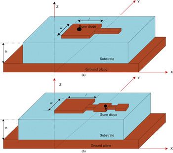
In an active antenna, there are two ways of mounting the Gunn diode on it. The central idea is, obviously, to realize the maximum radiated power from the antenna. It is not simply the question of finding the condition for maintenance of oscillations and the corresponding amplitude of oscillations. In the first instance (Fig. 1(a)), it is the position of the diode on the patch, where as in the second instance (Fig. 1(b)) it is related with the appropriate design of the microstrip transformer. Figure 1 shows the dimension of the active rectangular patch antenna.
Rectangular active microstrip patch antenna configuration in which the active device is placed on the patch (a) and is connected to the patch through a microstrip transformer (b).

Let the voltage output of the antenna be denoted by
 $$v\lpar t\rpar =V\lpar t\rpar \exp j\left({\omega _i t+\psi \lpar t\rpar } \right)\comma$$
where ψ (t) is the phase when frequency of oscillation is close to ωi. Now, the instantaneous frequency as [Reference Kurokawa23]
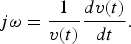 $$j\omega=\displaystyle{1 \over {v\lpar t\rpar }}\displaystyle{{dv\lpar t\rpar } \over {dt}}.$$
 $$\omega=\omega _i+\displaystyle{{d\psi } \over {dt}} - \displaystyle{j \over {V\lpar t\rpar }}\displaystyle{{dV\lpar t\rpar } \over {dt}}.$$
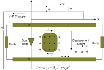
The conventional transmission line model of a microstrip patch is shown in Fig. 2. When the dc supply (V) is connected to the Gunn diode, the upper plate of the line acquires a positive charge, whereas the lower plate develops a negative charge. The unlike charges on the upper strip and lower ground plate establish a time-varying electric field between the plates. A closed current path is formed in which the current starts out at the plus terminal (upper strip), traverses the upper strip, short circuited at the wave front by the displacement current through the dielectric and returns through the ground plate to the anode terminal via the cathode terminal. Each time the transient current (i) flows through the diode in opposition to the dc direction, it develops a transient voltage v = i/αd. Here, αd is magnitude of the incremental negative conductance of the diode. The transient voltage will build up provided the intrinsic losses of the transmission line as well as the loss due to radiation through the ends of the transmission line are made by the negative conductance of the diode. This growth will be limited by the limiting-type non-linearity of the Gunn diode. Thus, after a while, the transient voltage will reach its limiting value. Once this limiting value is reached, the voltage will start discharging through the dielectric. As soon as this happens, the displacement current will start flowing in the opposite direction and the process will continue till the voltage attains the maximum negative value. Here, G r represents the radiation conductance and G m denotes the conductance due to mutual coupling between the opposite ends of the patch.
Transmission line model of active patch antenna.

Propagation constant of a low loss transmission line is
 $$\gamma=\alpha _j+j\beta _j=\sqrt {\left({R_1+j\omega L} \right)\left({G_j+j\omega C} \right)}\comma$$
where R 1 is the series intrinsic resistance. Now, G j the equivalent shunt conductance of a line of length l j can be written as
 $$G_j=G_i+{2G / l_j}.$$
Here, G is the total antenna conductance and G i is the intrinsic conductance; L and C are the inductance and capacitance per unit length of the transmission line, respectively. The input admittance at a point AB (Fig. 2) where the Gunn diode is connected is given by (considering  $\beta _1=\beta _2=\beta=\omega \sqrt {LC} $)
 $$\eqalign{Y_{in}&= G_{in}+jY_o \cr & \quad \times\left\{{\tan \beta l_1+\tan \beta l_2+\sqrt {LC} \displaystyle{{d\psi } \over {dt}} \left({l_1 \sec ^2 \beta l_1+l_2 \sec ^2 \beta l_2 } \right)} \right\}.}$$
At the steady state, Y in becomes [Reference Biswas, Bhattacharya, Mondal, Bose and Pal3]
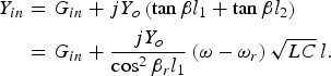 $$\eqalign{Y_{in}& =G_{in}+jY_o \left({\tan \beta l_1+\tan \beta l_2 } \right)\cr& =G_{in}+\displaystyle{{jY_o } \over {\cos ^2 \beta _r l_1 }}\left({\omega - \omega _r } \right)\sqrt {LC} \, l.}$$
Here, G in is the input shunt conductance per unit length, Y o is the output admittance, and β is the propagation constant. In (6), β is assumed to be nearly equal to  $\beta _r \, \lpar\! =\!\omega _r \sqrt {LC} \rpar $.
Equating (6) with dynamic impedance of diode and using (3), we obtain
 $${- \left({\displaystyle{I \over V}} \right)_{diode}=G_{in}+\displaystyle{{Cl} \over {\cos ^2 \beta _r l_1 }}\left[{j\left({\omega _i - \omega _r+\displaystyle{{d\psi } \over {dt}}} \right)+\displaystyle{1 \over V}\displaystyle{{dV} \over {dt}}} \right].}$$
Representing the diode current–voltage relation as [Reference Solbach15]
 $$i=- \alpha _d v+\beta _d v^2+\gamma _d v^3\comma \;$$
where, αd, βd and γd are diode constants with values of 0.0252, −0.01087 (at 9.5 V) and 0.0265, respectively.
From (7), we find that
 $$- \left({\displaystyle{I \over V}} \right)_{diode}=\left({ - \alpha _d+\displaystyle{3 \over 4}\gamma _d V^2 } \right).$$
Equating real and imaginary parts of equation (7) we can write the amplitude and phase equations of the antenna
 $$\displaystyle{{dV} \over {dt}}=\left({\displaystyle{V \over {Cl}}} \right)\left[{\left({\alpha _d - G_{in} - \displaystyle{3 \over 4}\gamma _d V^2 } \right)\cos ^2 \beta _r l_1 } \right]\comma$$
and
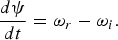 $$\displaystyle{{d\psi } \over {dt}}=\omega _r - \omega _i .$$
Combining expression (8) and (9) we obtain the steady-state output from an antenna as
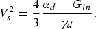 $$V_s^2=\displaystyle{4 \over 3}\displaystyle{{\alpha _d - G_{in} } \over {\gamma _d }}.$$
Power radiated
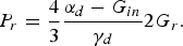 $$P_r=\displaystyle{4 \over 3}\displaystyle{{\alpha _d - G_{in} } \over {\gamma _d }}2G_r .$$
Maximum power radiated is found by putting, dP r/dG r = 0, which gives
 $$\alpha_d=\left[{4G_r - 2G_m+0.5\left({G_i+R_1 Y_o^2 } \right)\, l} \right]\sec ^2 \left({\beta _i l_1 } \right).$$
The value of αd is chosen to be the dynamic conductance of the diode. From this relation the value of l 1 i.e., location of the diode to obtain maximum radiated power is determined as
 $$l_1=\displaystyle{l \over \pi }\cos ^{ - 1} \sqrt {R_d \left\{{4G_r - 2G_m+0.5\left({G_i+R_1 Y_o^2 } \right)\, l} \right\}} .$$
The value of l 1 as given in [Reference Navarro and Chang10] is presented as
 $$l_1=\displaystyle{l \over \pi }\cos ^{ - 1} \sqrt {R_d \left({G_r - G_m } \right)}\comma$$
where  $R_d=\displaystyle{1 \over {\alpha _d }}. $
Now, maximum power becomes
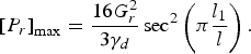 $$\left[{P_r } \right]_{\max }=\displaystyle{{16G_r^2 } \over {3\gamma _d }}\sec ^2 \left({\pi \displaystyle{{l_1 } \over l}} \right).$$
This indicates that the maximum power radiated is a function of the radiation conductance, non-linearity, and location of the diode.
III. COMPARISON OF DIFFERENT SETS OF PATCHES: EXPERIMENTAL RESULTS
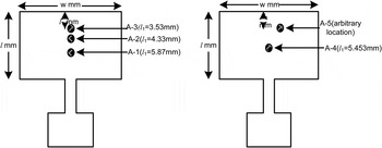
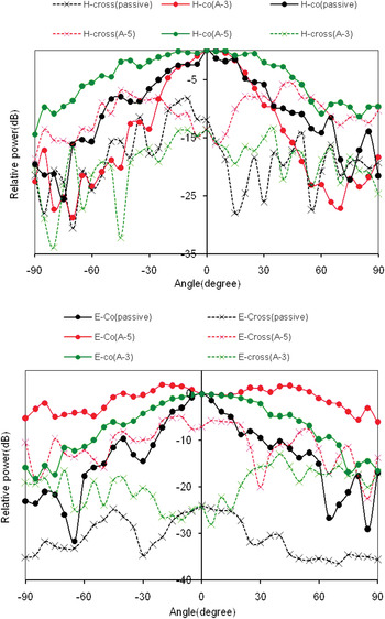
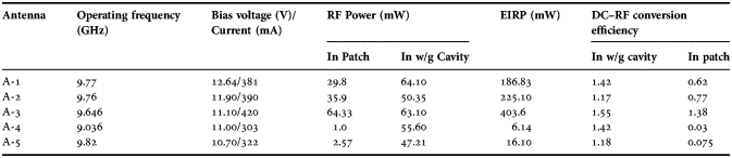
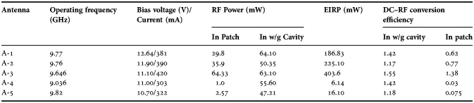
An active patch working at 9.5 GHz has been designed and fabricated with the help of photo-etching by using 0.787-mm thick Takonic TLY-5-0310-CH/CH substrate with ɛr = 2.2. The conducting material has 0.502/sq ft copper metallization with a metal thickness of 0.018 mm. The antenna is supported from the other side by a thick aluminum plate, which serves the purpose of heat sink as well as provides mechanical support for experimental observation. Two sets of five patches have been fabricated at two spot frequencies (f r) of 9.0 and 9.5 GHz by using 0.787-mm thick Takonic TLY-5-0310-CH/CH substrate with ɛr = 2.2. The entire scheme is shown in Fig. 3, where the diode positions have been measured from the top edge of the patches. For patches A-2 to A-4, the diodes have been placed at points (w/2, l 1), while the position of the diode on the patch A-1 is at (w/2, l–l 1). For the patch (A-5), the position of the diode on the patch is arbitrary (x, y). A screw-type low-power MA/COM-49104 Gunn diode has been used for the five patches to obtain a comparative picture. Radiation patterns are measured for three patches namely A-3, A-5, and a passive patch and are shown in Fig. 4. Table 1 lists the operational parameters of the antennas like frequency power etc. Power values have been calculated by using passive antenna gain to be 7.97 dBi. It is found from Table 1 that patch A-3 (l 1 = 3.53 mm) gives highest radiated power although the position of the diode on the patch should be A-2 (l 1 = 4.33 mm). When the diode is placed further up (l 1 < 3.53 mm), the radiated power is found to decrease along with significant deviation in operating frequency [Reference Chatterjee, Bhattacharaya and Biswas21].
Antenna configuration with diode at different positions.

Radiation pattern (co- and cross-polarization) of microstrip rectangular patch antenna.

Measured active antenna power and efficiency at the operating frequencies.
In order to calculate the value of frequency in Table 2 the following relation [Reference Biswas, Bhattacharya, Mondal, Bose and Pal3] is used:
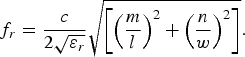 $$f_r=\displaystyle{c \over {2\sqrt {\varepsilon _r } }}\sqrt {\left[{\left({\displaystyle{m \over l}} \right)^2+\left({\displaystyle{n \over w}} \right)^2 } \right]} .$$
Calculated and measured operating frequencies for two set of five-patch antennas.

IV. HARMONICS IN ACTIVE MICROSTRIP PATCH ANTENNA
An active microstrip patch antenna combines the function of radio frequency (RF) generation and radiation in the same antenna element. However, it is beset with the problems of harmonic generation and to some extent spurious radiation [Reference Buesnel, Cryan and Hall16]. These adversely affect its operating efficiency and electromagnetic compatibility (EMC) implications. These problems are common to both the Field-effect transistor (FET) and Gunn/Impatt integrated microstrip patch antennas.
An active antenna can be represented by a large number of parallel resonant circuits. Experimental observation on the radiated field shows the presence of second harmonic component. Therefore in our analysis, the microstrip patch is represented by a series combination of two parallel resonant circuits: one is resonant at fundamental and other is at the second harmonic frequency. An active antenna (integrated with Gunn diode) basically operates on the principle of distributed parameter oscillator with the patch as distributed parameter circuit element and the diode as a non-linear negative resistance device. Owing to the non-linear current voltage characteristics of the Gunn diode and the harmonic resonant character of the microstrip patch, the system undergoes harmonic oscillations. The multiple resonant characteristic of the patch antenna can be easily explained with the help of cavity model as well as transmission line model. The system equations are written as [Reference Biswas, Bhattacharya, Mondal, Bose and Lahiri17]
 $${C_1 \displaystyle{{dv_1 } \over {dt}}+\displaystyle{1 \over {L_1 }}\int {v_1 dt+G_1 v_1+\left({ - \alpha _d v_1+\beta _d v_1 ^2+\gamma _d v_1 ^2 } \right)}=0\comma }$$
where, v 1 = V 1 cos (ω t + ψ) current–voltage relation of a Gunn diode has been used [Reference Biswas, Bhattacharya, Mondal, Bose and Lahiri17].
And
 $${C_2 \displaystyle{{dv_2 } \over {dt}}+\displaystyle{1 \over {L_2 }}\int {v_2 dt+G_2 v_2+\left({ - \alpha _d v_2+\beta _d v_2 ^2+\gamma _d v_2 ^3 } \right)}=0\comma }$$
 $$v_2=V_2 \cos \left({2\omega t+\theta } \right)\comma \;$$
where v 1, v 2 is the output voltage across the fundamental and the second resonant circuit. G 1 and G 2 are the equivalent input conductance of a patch working at ω and 2ω, respectively, and are given by
 $$G_1=\left[{2\left({G_r - G_m } \right)+0.5\left({R_1 Y_o^2+G_i } \right)\; l} \right]\sec ^2 \left({\beta \; l_1 } \right)\comma \;$$
 $$G_2=\left[{2\left({G^{\prime}_r - G^{\prime}_m } \right)+0.5\left({R^{\prime}_1 Y_o^2+G^{\prime}_i } \right)\; l} \right]\sec ^2 \left({2\beta \; l_1 } \right)\comma \;$$
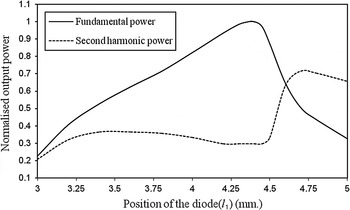
where un-primed and primed quantities are the corresponding parameters for a patch working at ω and 2ω, respectively. Variation of the fundamental and the second harmonic power with the position of the diode (l 1) is obtained through computer simulation. The result is plotted in Fig. 5. Simulation results indicate that the value of l 1 (at which fundamental Power is the maximum) is very close to the value where the second harmonic power is maximum. Theoretical exercise is based on the assumption that the diode is a point source. In practice, it is not so, e.g. for an MA/COM 49104 diode, dimension is 0.15 × 0.15 mm. Therefore, the suggested equation for locating diode is
 $$l_1=\left[{l_1 } \right]^{max} - \displaystyle{{{\rm diode}\; {\rm diameter}} \over 2}.$$
Variation of relative fundamental and second harmonic power with the position of diode along the length of a rectangular active patch designed to oscillate at 9.5 GHz.

V. INJECTION LOCKING
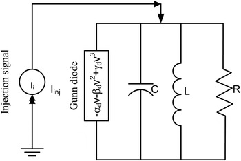
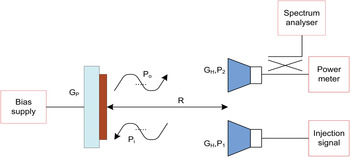
Active antenna acts as a transmitter as well as a receiver and for its faithful operation it is necessary to generate near noise-free oscillations. Improvements of the oscillator phase jitter and oscillator stability, thus, are important consideration. Techniques such as injection-locking dielectric resonators, tuned cavities, etc. are usually used to improve frequency stability and phase noise characteristics. In this section, a combination of injection and phase locking through bias control has been proposed. The arrangement is shown in Fig. 8. It consists of a rectangular active patch antenna, a balanced mixer-type phase-sensing device, and a bias control arrangement. A sinusoidal signal of frequency ω1 acting on a nearly sinusoidal oscillator of frequency ωo affects its behavior in many respects depending on the strength and frequency of the forcing signal. A forcing signal when injected into an oscillator modifies its properties in many ways. The analytical equivalent circuit of an oscillator under the influence of a forcing signal is represented in Fig. 6. Within the synchronization range the locked oscillator loses its identity and obeys commands from the forcing signal, and the oscillator is said to be injection locked (phase locked) to the synchronization signal. Injection-locked oscillators (ILOs) find many uses in practice. It can be used (1) to reduce the depth of modulation of an amplitude modulation (AM) signal, (2) as frequency modulation (FM)–AM converter, (3) as an amplifier for angle-modulated signals, etc. An active microstrip patch integrated with a Gunn diode can be used as an injection-locked Gunn oscillator (ILGO). Detection of an information signal in the presence of co-channel interference has been performed in this section. Injection-locking technique is efficient to demodulate the signal [Reference Chatterjee and Biswas22].
Equivalent circuit of an ILO.

A parallel equivalent circuit of a Gunn oscillator in the presence of an injection-locking signal is shown in Fig. 6. Let
 $$I_{inj}=I\cos \left({\omega _c t+\theta } \right)\comma$$
where θ = msin(ωmt), represents an FM signal at X-band shining on the active antenna. The equation of a negative resistance oscillator in the presence of injected microwave FM signal can be written as [Reference Biswas9]
 $${\displaystyle{1 \over L}\int {v\left(t \right)dt+C\displaystyle{{dv\left(t \right)} \over {dt}}}+G_1 v\left(t \right)- \alpha _d v\left(t \right)+\gamma _d v\left(t \right)^3=I_{inj}\comma}$$
where L, C, G 1 are inductance, capacitance and conductance of the parallel tuned circuit, respectively; αd, γd are constants of Gunn diode; and I is the current strength of the carrier signal.
Suppose that the carrier frequency of the injected FM signal is close to the free running frequency of the oscillator. Output of the locked antenna is assumed to be of the form
 $$\nu \lpar t\rpar =V\lpar t\rpar \cos \left({\omega _o t+\theta _o \left(t \right)} \right)\comma$$
 $$\varphi=\theta - \theta _o .$$
V is the voltage amplitude of the locked antenna and ϕ is the phase error. Substituting (21) and (22) into (20) and applying the principle of harmonic balance, we obtain the following amplitude and phase equations of the ILGO:
 $$\displaystyle{{dV} \over {dt}}=\displaystyle{{\omega _o V} \over {2Q}}\left({\alpha _k - \displaystyle{3 \over 4}\gamma _k V^2 } \right)+\displaystyle{{\omega _o } \over {2Q}}E\cos \phi\comma$$
 $$\displaystyle{{d\phi } \over {dt}}=\displaystyle{{\omega _o } \over 2}\left({\displaystyle{{\omega _c } \over {\omega _o }} - \displaystyle{{\omega _o } \over {\omega _c }}} \right)- \displaystyle{{\omega _o } \over {2Q}}\left({\displaystyle{E \over V}} \right)\sin \phi+\displaystyle{{d\theta } \over {dt}}\comma$$
where −R(αd − G 1) = αk and Rγd = γkm and ωm are the modulating index and modulating frequency of the FM signal, ωo is resonance frequency of the oscillator, Q is the quality factor of the oscillator; and E is the strength of the injection.
Now, locking range of the ILO can be expressed as
 $$k=\displaystyle{{\omega _o } \over {2Q}}\displaystyle{E \over V}\comma$$
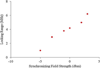
It is revealed by (25) that the lock range is directly proportional to the strength of the injection signal and inversely proportional to the quality factor of the Inductance and Capacitance (LC) tank. Increasing the amplitude of injection signal E, although increasing the lock range, is at the cost of power consumption. Figure 7 shows the variation of locking range with synchronized field strength obtained using the experimental arrangement as depicted in Fig. 8. Figure 7 supported the theoretical finding.
Experimental value for locking range with synchronized field strength.

Injection-locking arrangement.

VI. CONCLUSION
An expression (13) for determining the position of the diode within the rectangular patch has been proposed in this paper on the basis of maximum radiated power. The result was compared with the available literature [Reference Navarro and Chang10] given in (14). Knowing the values of diode constants, one can easily find out the maximum radiated power (15). It is further observed that the location of the diode at which the fundamental power is maximum, is not the position of minimum second harmonic generation [Reference Buesnel, Cryan and Hall16, Reference Biswas, Bhattacharya, Mondal, Bose and Lahiri17]. Moreover, a commercially available diode has a finite dimension, not a point source. When the diode is placed at the point where the fundamental power is maximum it infringes into the susceptible zone of second harmonic oscillations. Therefore, the diode has been placed so as to avoid the susceptible zone of second harmonic oscillations. Fortunately, it has been found that in doing so, the generation of fundamental power is not much affected. Expression (13) has therefore been modified to (18), so that the power output and EMC conditions are optimum. With this arrangement, power output from an active antenna designed to operate at 9.5 GHz was 64.33 mW (Effective Isotropic Radiated Power (EIRP) ~403.6) almost equal to waveguide tuned oscillator. The frequency error is 1.54%, which also confirmed the proper design of the patch. Conversion efficiency (DC to RF) achieved was 1.38% in contrast to 1.55% when the diode has been placed in a waveguide. Owing to the perfect matching between the device and antenna a large Q value has been realized (~156). Bias-tuning bandwidth of such a rectangular patch is only 2.16% which is very low and is one of the disadvantages of active microstrip patch antenna. A 10.198 × 12.283 mm2 rectangular patch exhibited a locking gain of 25 dB, a locking range 3.6 MHz at 9.799 GHz. As the injection lock power decreases, there is a corresponding decrease in obtainable bandwidth. A notable improvement in signal quality has been observed even in the free running mode in comparison to others [Reference Chang, Hummer and Klein14, Reference Liu, Shi and Liu19].
 Somnath Chatterjee received his B.Sc. and M.Sc. degrees in Physics from Burdwan University, West Bengal, India in the year 1998 and 2001, respectively. Recently, he submitted his Ph.D. thesis from West Bengal University of Technology. He received the URSI Young Scientist Award of the International Union of Radio Science in the year 2005 and has authored 15 international peer reviewed journal papers. At present, Mr Chatterjee is with the Kanailal Vidyamandir (French Section), Chandernagore as a Headmaster/Principal. His areas of interests include active microstrip patch and slot antenna; optoelectronic oscillator, and Injection-locked oscillator etc.
 Susmita Pal (Born December 26, 1969) received the Bachelor's Degree in Electronics and Telecommunication Engineering from Burdwan University in 1992 and received the Master's Degree in Communication Engineering from Jadavpur University in 1994. She received the URSI Young Scientist Award of the International Union of Radio Science in the year 1996. She also received the KS Krishnan Memorial Award 1995 from the Council of the Institution of Electronics and Telecommunication Engineers (IETE) for the best system oriented paper entitled “A new DSP-DPLL demodulator with a difference”. Her areas of interest include Fiber Optics and Optical Microwave Interactions. She has co-authored seven research papers. She is currently working as a Project Engineer in Webel Electronic Communication Systems Limited, Kolkata.
 Apala Bhattacharaya received her B.Sc. and M.Sc. degree in Physics from Burdwan University, West Bengal, India in the year 1992 and 1994, respectively. She received her Ph.D. from Burdwan University. Ms Bhattacharaya was the recipient of URSI Young Scientist awards in 2005 and author of 18 international peer reviewed journal papers. At present Ms Bhattacharaya is with the Vivekananda Mahavidyalaya, Burdwan as an assistant professor. Her research interests are in active microstrip patch, Microwave oscillator and Injection-locked oscillator.
 B N Biswas is an Emeritus Professor, Chairman, Education Division SKF Group of Institutions, former National Lecturer (UGC), Emeritus Fellow (AICTE) Visiting Faculty University of Minnesota (USA); Founder Prof-in-Charge University Institute of Technology, Microwave Division (BU); CU Gold Medalist; URSI Member: Commissions C, D, E and Developing Countries, Seminar Lecture tour to: University of Pisa (Italy), University of Bath (UK), University College (London), University of Leeds (UK), University of Kyoto (Japan), University of Okayama (Japan), Electro Communication University (Osaka), Czech Academy of Sciences; University of Erlangen (Germany), National Singapore University etc; Best Citizens Award (2005); Member: Various National & International Committee, Recipient of Various Awards. Supervised 22 Ph.D. students and is the author of 235 Publications in IEEEs and other referred journals.