Introduction
The design and operation of advanced synchrotron light beamlines rely on the availability of near-perfect optical elements, some of which are used to collimate or focus the incident beam. Common focusing elements Reference Ice, Budai and Pang1 include bent crystals, multilayers or mirrors, capillaries, waveguides, refractive lenses, and diffractive elements such as Fresnel zone plates or multilayer Laue lenses. Focused beam sizes on the order of a few micrometers are now routinely achieved; focused beam sizes of a few tens of nanometers were recently obtained at some experimental stations.
This article examines focusing x-ray optics that exploit refraction mechanisms. The first lens of this type, a compound refractive lens (CRL), was proposed in 1994 Reference Tomie2 and employed in 1996. Reference Snigirev, Kohn, Snigireva and Lengeler3 Since then, CRLs have become widespread. An overview of previously and currently used x-ray lenses, ordered by manufacturing technique, is available in the Supplementary Material, available online. CRLs have several advantages. (1) They occupy a very small footprint; (2) they do not cause deviations in beam direction; and (3) they do not require any sorting apertures for suppression of unwanted diffraction orders. Moreover, they are easy and fast to align, and obtaining a microfocused beam for energies E ≥ 2 keV Reference Wilhelm, Garbarino, Jacobs, Vitoux, Steinmann, Guillou, Snigirev, Snigireva, Voisin, Braithwaite, Aoki, Brison, Kantor, Lyatun and Rogalev4 is straightforward.
Focusing and absorption of x-rays in the lens material is described by the refractive index: Reference Snigirev, Kohn, Snigireva and Lengeler3
 $$n = 1 - {\rm{\delta }} + {\rm{\beta ,}}$$
where δ is the real part of the refractive-index decrement, which is responsible for refraction. In the imaginary part, β is the absorption coefficient, which is responsible for the attenuation of the beam (due to absorption and scattering caused by the photoelectric effect and the Compton effect) of x-rays in the material. For hard x-rays, the dependence on the material is approximated by
 ${\delta \over \rho } \propto {\rm Z}$
and
 ${\beta \over \rho } \propto {{\rm Z}^3}$
with Z being the atomic number and ρ the element density. Materials with low Z, but high density are, therefore, desired candidates for CRLs.
Reference Serebrennikov, Clementyev, Semenov and Snigirev5
The refractive-index real-part decrement δ is a small number (∼10−5−10−6). Therefore, refractive lenses are fabricated with a pronounced curvature, and a series of stacked refractive surfaces are needed in order to produce a relatively short focal length (this is the origin of the word “compound” in CRL). Absorption in the thicker parts of the lens limits the practical numerical aperture (NA), defining the optics opening angle.
For thin CRLs (lens stack length << f), the focal length f is given by: Reference Snigirev, Kohn, Snigireva and Lengeler3
 $$f\, = \,{R \over {N\delta }},$$
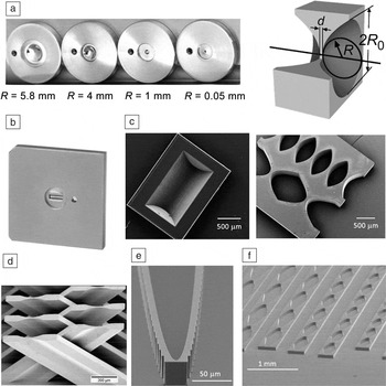
where R is the radius of curvature at the apex of the refractive surfaces and N is the number of refractive surfaces. Fabrication methods, materials, and geometry of x-ray lenses are varied; see Figure 1 and also Table I in the online Supplementary Material. CRLs, which can be both two-dimensional (2D) and one-dimensional (1D) focusing, are often assembled in the form of transfocators—which allow the insertion of a selected subset of lenses from a pool of lenses into the x-ray beam—for versatility in focal length and energy selection. Reference Vaughan, Wright, Bytchkov, Rossat, Gleyzolle, Snigireva and Snigirev6 Nanofocusing lenses Reference Aristov, Grigoriev, Kuznetsov, Shabelnikov, Yunkin, Hoffmann and Voges7,Reference Schroer, Kurapova, Patommel, Boye, Feldkamp, Lengeler, Burghammer, Riekel, Vincze, van der Hart and Küchler8 fabricated with lithographic and microfabrication methods are often planar (1D focusing). A large number of lenses, all built on the same chip, can provide different focal lengths, apertures, geometrical parameters, and be used at different x-ray energies.
Different x-ray lens types. (a) Two-dimensional parabolic and (b) 1D parabolic Be lenses (made by RXOPTICS). (c) Diamond lenses machined by laser ablation. (d) Crossed-2D SU-8 polymer lenses. (e) Single kinoform Si lens and (f) parabolic diamond lenses.

Refractive lenses are shaped to obtain aberration-free designs. Reference Schroer and Lengeler9,Reference Sanchez del Rio and Alianelli10 Fabrication methods and materials are, however, not perfect, and the presence of roughness or figure error—deviation of the lens shape from the ideal shape—is quite common. Focusing is affected by the quality of the lens material and the amount of material traversed by the beam. Unlike in grazing incidence optics, the spatial resolution (i.e., the minimum spot size of the focused beam) of refractive focusing lenses is not directly proportional to the figure error of the shape. However, unwanted scattering from small-angle x-ray scattering and Compton scattering leads to blurring, thus reducing the resolution of the lens or the x-ray peak flux. Efforts to increase the NA for lenses with short focal length have resulted in new designs and fabrication methods, in particular, low absorption kinoform lenses made of single-crystal material. Reference Aristov, Grigoriev, Kuznetsov, Shabelnikov, Yunkin, Hoffmann and Voges7,Reference Evans-Lutterodt, Ablett, Stein, Kao, Tennant, Klemens, Taylor, Jacobsen, Gammel, Huggins, Ustin, Bogart and Ocola11,Reference Alianelli, Sawhney, Barrett, Pape, Malik and Wilson12 (A kinoform lens is shown in Figure 1e). These lenses are characterized by the removal of lens material in steps of length h, such that the phase difference ∆φ = φlens(ℎ) − φair(ℎ) experienced by an x-ray photon is an integer multiple of 2π, where φlens(ℎ) and φair(ℎ) is the induced phase shift after propagation of a distance ℎ in the lens or in air, respectively.
Required properties for x-ray lenses minimizing wavefront distortions
New experimental methods such as coherent x-ray diffraction imaging (CDI), scanning CDI (known as ptychography), x-ray photon correlation spectroscopy, and imaging of phase objects in general, are enabled by increased coherence of x-ray beams. X-ray optics designed for such applications should produce a localized and flat wavefront at the sample and must avoid the appearance of speckle patterns produced by the optic itself. An important question is whether refractive lenses made with imperfect materials are detrimental to the wavefront shape of the focused beam and to what extent.
Important for any lens at x-ray or optical wavelengths is the lens shape and its surface roughness, as well as the homogeneity of its material. With homogeneity, we refer to the internal lens structure, which could contain inclusions, voids, and grain boundaries; the structure could be crystalline or amorphous. As for the crystallinity, it can be single crystalline or polycrystalline, showing a distribution in the size of its constituent nano- or microcrystals.
Shape errors
X-ray lenses without geometrical aberrations and with a sufficiently large aperture will focus an x-ray source into an ideal Gaussian profile in the focal plane. Deviations from the desired lens shape will result in a non-Gaussian beam profile at the focus and, in general, inhomogeneous beam shapes outside the focal plane. Side lobes of the beam in the focal plane will prohibit scanning probe experiments such as fluorescence imaging. CDI experiments are easier to analyze with a Gaussian probe beam.
Beryllium lenses, for example, can be pressed into a close-to-parabolic shape, featuring maximum deviation from the ideal paraboloid shape of less than 0.5 µm; Reference Seiboth, Schropp, Scholz, Wittwer, Rödel, Wünsche, Ullsperger, Nolte, Rahomäki, Parfeniukas, Giakoumidis, Vogt, Wagner, Rau, Boesenberg, Garrevoet, Falkenberg, Galtier, Lee, Nagler and Schroer13 see the section titled “Possibility to correct for an imperfect lens shape” in this article for more information. Lithography techniques instead allow for a maximum deviation from the ideal paraboloid shape of less than 0.05 µm.
Homogeneity
While a single-crystalline material will give a minimal small-angle x-ray scattering (SAXS) background, it might be prone to x-ray losses due to the accidental fulfilment of Bragg’s Law resulting in Bragg reflection. This especially becomes important if many individual lenses are assembled into a CRL. A polycrystalline material with individual crystals of micro- or nanometer size reduces the probability of intense, unwanted Bragg-diffracted x-rays, Reference Goto, Yabashi, Tamasaku and Ishikawa14 but some intensity will be lost into powder diffraction rings. On the other hand, an amorphous material will show neither x-ray powder diffraction rings, nor accidental Bragg reflections, but the loss to SAXS can be significant.
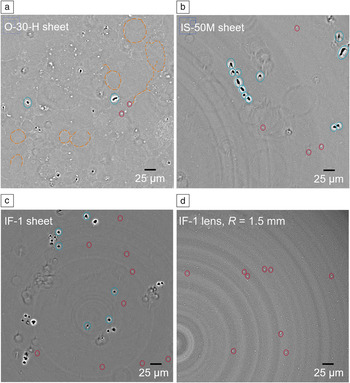
Many materials include voids and inclusions in their bulk (see Figure 2 ), such as in different grades of Be. Reference Roth, Helfen, Hallmann, Samoylova, Kwaśniewski, Lengeler and Madsen18 Each void or inclusion acts as a pinhole of different electron density that diffracts the beam and leads to the propagation of diffraction rings toward the sample, distorting the wavefront. If different grades of a material were available, one could select the material with the best x-ray properties. However, this might not always be the grade providing the best lens with the employed manufacturing process.
X-ray laminography slices through different Be grades (O-30-H, IS-50M, and IF-1) and a pressed lens made of IF-1 grade Be. Reference Roth, Helfen, Hallmann, Samoylova, Kwaśniewski, Lengeler and Madsen18 (a) The powder-metallurgy grade shows voids (blue), inclusions (red), and oxygen-decorated boundaries (yellow) between the individual powder grains. (b–c) The hot-rolled grade foil shows only voids and inclusions. (d) Laminography slice through the center of an IF-1 foil and through the center of the finished lens (made by RXOPTICS). The voids disappear during the lens-pressing procedure.

Surface roughness
When a coherent x-ray wavefront travels through a lens air or lens vacuum interface, it will acquire a local phase shift φ(x, y) depending on the local surface height h(x, y), similar to when it passes through a void inside the lens. This means that the local height variation at the interface should be limited. As the beam travels almost perpendicular to the interface, and not at grazing incidence as with mirror optics, the surface roughness does not need to adhere to the same degree of perfection. Lenses are less sensitive to surface roughness by roughly a factor of 103 compared to mirrors, and a vertical roughness as high as 0.1 µm can be tolerated. Reference Lengeler, Schroer, Tümmler, Benner, Richwin, Snigirev, Snigireva and Drakopoulos15
Other requirements
Finally, the lens materials must be radiation hard (which is not the case for many organic materials) and often vacuum-compatible, with good thermal conductivity, and, ideally, a high melting point. When comparing materials with respect to the heat evacuation problem (the incident x-ray beam will get partially absorbed in the lens material, leading to a temperature rise that will be balanced by heat transfer to the surrounding [e.g., the lens container and its clamping]) common in modern storage rings and x-ray free-electron lasers (XFELs), it is important to consider the ratio κ/µ, where κ is the thermal conductivity and µ is the absorption coefficient, rather than κ alone. In this regard, diamond lenses present an advantage.
Current x-ray refractive lens materials
Different manufacturing techniques are currently used to produce x-ray lenses. Most of these techniques work well for a specific set of materials. A table of lens materials, listed by the manufacturing technique, is presented in the supplementary material, available online, together with the commonly used characterization methods to test the lens quality.
Pressed lenses
Rotationally symmetric 2D and large 1D lenses can be fabricated using a pressing technique, where two negatively shaped dies indent into a flat disc, producing a doubly concave x-ray lens. The pressing technique works well for metals such as Be, Al, and Ni. It produces lenses with relatively large aperture with radii greater than 50 µm that are capable of focusing a wide beam, either along one transverse direction (1D lenses) or along both transverse directions (2D lenses).
Beryllium
Be is brittle at room temperature, but when heated above 800°C, it can be plastically deformed. Reference Tümmler16 The initial Be substrates (in the form of a plate) are obtained from different metallurgical grades that can be classified in two groups—Be grades issued from powder metallurgy (such as Materions I-70-H, O-30-H) and those obtained from hot rolling (IF-1 and IS-50M). Reference Dombrowski17 The former involves chipping a Be ingot into smaller grains followed by attrition milling or grinding and later compaction under vacuum. During that process, the grains tend to oxidize, which is observable using x-ray laminography (a specific x-ray tomography method), where the boundaries of the initial grains are visible. The hot-rolling method avoids the chipping and grinding step, and instead rolls the Be ingot at an elevated temperature. The resulting Be sheet is limited in thickness, especially for the IF-1 grade, thereby limiting the lens thickness and the physical lens aperture. X-ray laminography no longer reveals oxygen-decorated boundaries between the powder grains. Instead, voids with sizes of a few microns are visible. Fortunately, these disappear once the Be is pressed into the lens shape. Figure 2 shows cuts through different Be grades and a pressed IF-1 lens. Reference Roth, Helfen, Hallmann, Samoylova, Kwaśniewski, Lengeler and Madsen18 The difference in microstructure is evidenced also in SAXS measurements, Reference Roth, Helfen, Hallmann, Samoylova, Kwaśniewski, Lengeler and Madsen18,Reference Lyatun, Goikhman, Ershov, Snigireva and Snigirev19 again showing better suitability of the hot-rolled grades.
Be lenses are polycrystalline. The size of the crystal grains in Materion Be grades is in the range of 5–15 µm. Single-crystalline Be would not remain single crystalline after the lens-forming step, but efforts are taken to reduce the crystallite size into the nanometer regime. Typical surface average roughness (R a) of 2D Be lenses is on the order of 0.02 µm.
Aluminum
A nontoxic alternative to pressed Be lenses is aluminum. The shape-fidelity with Al lenses is good and better than that of Be. Reference Tümmler16 Aluminum lenses have the disadvantage of a much higher x-ray absorption for low-energy x-rays, which limits their use to above 40 keV x-ray energy.
Nickel
For very high x-ray energies ( >80 keV), pressed 1D Ni lenses are occasionally employed. Reference Andrejcuk, Sakurai and Itou20 Higher-Z materials are necessary for the focusing of very high x-ray energies, as otherwise too many lens elements are needed.
Planar lenses produced by lithography
Micromachining methods using lithography followed by etching and the lithographie, galvanoformung, abformung (LIGA) technique are capable of producing lenses fabricated with high accuracy and resolution. Reference Nazmov, Reznikova, Last, Mohr, Saile, Simon and DiMichiel21 They are mostly planar, 1D lenses of limited aperture in the direction perpendicular to the substrate plane, but allow for much smaller radii and are thus well adapted for nanofocusing. However, absorption limits the aperture of nanofocusing lenses, with kinoform lenses overcoming this issue to some extent. Micromachining has been used to fabricate lenses in Si, Ge, the polymers SU-8 and PMMA, and Ni via LIGA. It was also used to make Si molds needed as templates for growing polycrystalline diamond lenses.
Silicon
Advanced methods of dry etching, based on Bosch cyclic and cryogenic processes, are used to make planar silicon lenses with scalloping less than 20 nm in amplitude (meaning smooth vertical side walls), and aspect ratios as high as 50:1. Reference Walker22 Because of high x-ray absorption in silicon, the Si lens structures must be very thin (minimizing the amount of material). This, together with wall tapering during the etch, limits the total height of Si lenses. Due to its single-crystalline structure and thus low SAXS background, and despite fabrication and NA issues, silicon lenses have provided some of the highest quality nanofocusing lenses Reference Schroer, Kurapova, Patommel, Boye, Feldkamp, Lengeler, Burghammer, Riekel, Vincze, van der Hart and Küchler8 and are used for nanoprobe experiments (beams of 50 nm and below). Silicon etching is potentially capable of delivering even shorter focal length optics, both for the simple parabolic design Reference Schroer and Lengeler9 or the kinoform design. Reference Alianelli, Sawhney, Barrett, Pape, Malik and Wilson12,Reference Evans-Lutterodt, Stein, Ablett, Bozovic, Taylor and Tennant23 Advances in nanolithography could lead to lenses with focal lengths of only few mm and NAs greater than the current 10−3 limit.
Diamond
One of the most desirable materials for x-ray optics is single-crystal diamond. Unfortunately, diamond is unavailable as large high-quality single crystals, and is nearly impossible to etch. Reference Isakovic, Stein, Warren, Narayanan, Sprung, Sandy and Evans-Lutterodt24 Deposition of micro- and nanocrystalline diamond into silicon templates with a final etch of the template away from the diamond has achieved high-conformity lenses. Complete filling of the trenches in the silicon template with diamond crystallites is possible with this method. Much improved efficiency from diamond lenses (as compared to silicon) is inferred from experimental data—both effective aperture and transmitted flux are 2× larger with diamond under the same experimental conditions. Reference Fox, Alianelli, Malik, Pape, May and Sawhney25 Scattering from the polycrystalline material has so far prevented a sharp focus due to a large x-ray background, 210 nm being the smallest spot size measured to date. Reference Fox, Alianelli, Malik, Pape, May and Sawhney25 However, by reducing the amount of material in the lens with a kinoform design, smaller beam sizes at the focus should be possible.
SU-8 and PMMA
Deep x-ray lithography Reference Nazmov, Reznikova, Last, Mohr, Saile, Simon and DiMichiel21 in SU-8 or PMMA resists delivers lenses with larger dimensions and higher aspect ratios than silicon. The surface roughness is relatively small. The low heat conductivity and melting point of these materials, together with their SAXS signal, make them less attractive than lenses made of metal or single-crystal silicon. Their main benefit, however, is the large structure height achievable with deep x-ray lithography.
Lamellar lenses
To fabricate lenses out of materials only accessible using thin-film techniques such as Al2O3 via atomic layer deposition, a new lens shape with constant material thickness has been developed. Reference Seiboth, Scholz, Patommel, Hoppe, Wittwer, Reinhardt, Seidel, Knaut, Jahn, Richter, Bartha, Falkenberg and Schroer26 The shape creates a concave lens not by a parabolic thickness profile, but rather, by a distinct bending of a lamella with constant thickness. The Al2O3 lens material is coated onto a Si scaffold that is then removed using an etch after the coating.
Fabrication of diamond lenses by laser ablation
Recently, it has become possible to machine synthetic diamond (both high-pressure high-temperature grade and chemical vapor deposited grade), using pico- and femtosecond pulsed UV laser sources to remove carbon from the diamond surface via ablation. These techniques have been employed to create large individual 2D Reference Terentyev, Blank, Polyakov, Zholudev, Snigirev, Polikarpov, Kolodziej, Qian, Zhou and Shvyd’ko27,Reference Antipov, Baryshev, Butler, Antipova, Liu and Stoupin28 or 1D Reference Polikarpov, Snigireva and Snigirev29,Reference Terentyev, Polikarpov, Snigireva, Di Michiel, Zholudev, Yunkin, Kuznetsov, Blank and Snigirev30 diamond lenses and 1D planar lens arrays Reference Polikarpov, Snigireva, Morse, Yunkin, Kuznetsov and Snigirev31 in a single-crystalline diamond. Polycrystalline diamond is also used. Reference Kononenko, Ralchenko, Ashkinazi, Polikarpov, Ershov, Kuznetsov, Yunkin, Snigireva and Konov32 Laser ablation shows much promise, but the roughness of the laser-ablated surfaces must be improved, with current achieved averaged roughness down to R a = 0.3 µm. Also, laser ablation can graphitize the surface region, Reference Terentyev, Polikarpov, Snigireva, Di Michiel, Zholudev, Yunkin, Kuznetsov, Blank and Snigirev30 which should result in SAXS intensity losses.
Similar to single-crystalline Si, accidental fulfilment of Bragg’s condition will diffract part of the beam away from the optical axis, and glitches appear in transmission during an energy scan. Reference Terentyev, Polikarpov, Snigireva, Di Michiel, Zholudev, Yunkin, Kuznetsov, Blank and Snigirev30
Potential new lens materials
Serebrennikov et al. Reference Serebrennikov, Clementyev, Semenov and Snigirev5 investigated theoretically possible future binary (composed of two elements) lens materials with respect to focusing capabilities and absorption and found beneficial properties in B4C, cubic BN, and LiB. Binary materials involving even minor amounts of high-Z elements are shown to be inefficient. B4C is radiation hard and is commonly used for XFELs optics such as a mirror coating or for pre-absorbers. Unfortunately, it shows a high SAXS background. Reference Tümmler16 Machining of cubic BN or LiB lenses has not been attempted.
Possibility to correct for an imperfect lens shape
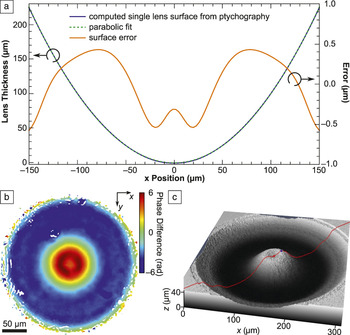
X-ray ptychography has been applied to measure the complex wavefront created by a Be CRL, and to recover the shape error of that lens stack. Reference Seiboth, Schropp, Scholz, Wittwer, Rödel, Wünsche, Ullsperger, Nolte, Rahomäki, Parfeniukas, Giakoumidis, Vogt, Wagner, Rau, Boesenberg, Garrevoet, Falkenberg, Galtier, Lee, Nagler and Schroer13,Reference Seiboth, Kahnt, Scholz, Seyrich, Wittwer, Garrevoet, Falkenberg, Schropp and Schroer33 The CRL stack comprised N = 20 2D parabolic IF-1 grade lenses (made by RXOPTICS) with apex radius R = 50 µm. The geometric aperture was 300 µm. Analysis of the ptychographic data showed that each lens surface on average deviates from the ideal parabola by about ±0.5 µm over an aperture of 300 µm ( Figure 3a).
(a) Reconstructed lens profile and error. (b) Reconstructed phase error of the beam exiting an N = 20 lens stack. (c) SiO2 phase plate to correct for the aberration.

It is possible to correct the distorted wavefront at the exit of the lens stack (see Figure 3b) by using a phase plate (i.e., a correcting lens). This requires a single-element high-precision correcting lens instead of improving the shape of N = 20 parabolic lenses. Such correcting lenses have been fabricated by ultrashort-pulsed laser ablation (see Figure 3c). Reference Seiboth, Schropp, Scholz, Wittwer, Rödel, Wünsche, Ullsperger, Nolte, Rahomäki, Parfeniukas, Giakoumidis, Vogt, Wagner, Rau, Boesenberg, Garrevoet, Falkenberg, Galtier, Lee, Nagler and Schroer13 By adding this phase plate after the CRL stack, the authors generated a diffraction-limited beam with a Gaussian focal spot. The correcting lens, however, is specific to that N = 20 CRL stack, and would have to be remeasured and refabricated for a different CRL stack.
Outlook
Beryllium will remain the main lens material for most standard focusing and many nanofocusing applications at synchrotron sources. Their quality and ease of use (inline optics) are well suited at synchrotrons worldwide to obtain micrometer-sized focal spots. Efforts are ongoing to further improve the shape fidelity and quality of pressed Be lenses.
Heat-load issues experienced by the optical elements at future high-repetition XFELs will foster continuing efforts in lens fabrication using diamond, where the biggest issues remain the surface roughness, which needs to be significantly reduced, and cost. Once the surface roughness issue is solved, laser machining could, in principle, also yield 2D kinoform lenses (e.g., 2D lenses with minimized absorption). It would make sense to apply laser ablation machining also to nondiamond materials.
We also assume that technology in both reductive and additive micromachining will advance to such precision that 1D x-ray lenses with details of a few tens of nanometers can be fabricated, making x-ray refractive optics more competitive in the ultrashort focal length range.
Finally, three-dimensional (3D) printing techniques Reference Vaezi, Seitz and Yang34 should soon achieve precision and surface roughness compatible with x-ray lenses. This will enable 3D-printed 2D kinoform lenses. A severe drawback of such lenses could, however, be their inhomogeneous internal structure, caused by layer-by-layer machining.

Thomas Roth is an x-ray optics specialist at the European Synchrotron Radiation Facility (ESRF), France. He obtained his PhD degree in physics from the University of Darmstadt, Germany. He was a postdoctoral researcher at The University of British Columbia, Canada, and then returned to work at ESRF at the Techniques and Instrumentation Test beamline ID06. Prior to his current position, he participated in designing the Materials Imaging and Dynamics endstation at the European X-ray Free Electron Laser, Germany. Roth can be reached by phone at +33 476882366 or by email at thomas.roth@esrf.fr.

Lucia Alianelli has been a senior optics scientist at the Diamond Light Source, UK, since 2004. She received her MS degree from the University of Florence, Italy, and her PhD degree in physics from the Université Joseph Fourier, France. She studied at the Institut Laue-Langevin, France, first as a doctoral candidate, and then as a postdoctoral research associate. Her research interests include x-ray beamline optical design and focusing optics development. Alianelli can be reached by phone at 01235 778252 or by email at lucia.alianelli@diamond.ac.uk.

Daniel Lengeler joined RXOPTICS, Germany, in 2015. He studied computer science, physics, and mathematics at RWTH Aachen University, Germany, and the University of Freiburg, Germany, where he received his PhD degree in the field of modeling, analysis, and numerics of partial differential equations. He completed his postdoctoral research at the University of Regensburg, Germany. He was a member of the SFB TR 71: Geometric Partial Differential Equations and the SPP 1506: Transport Processes at Fluidic Interfaces research programs. Lengeler can be reached by phone at +49 2461 9316065 or by email at daniel.lengeler@rxoptics.de.

Anatoly Snigirev is head of the X-ray Optics Laboratory at the Baltic Federal University, Russia. He received his PhD degree in physics from the Institute of Solid State Physics, Russian Academy of Sciences (RAS), in 1986. From 1986 to 1993, he was a staff scientist, and then head of the X-ray Crystal Optics Group in the Institute of Microelectronics Technology, RAS. From 1993 to 2015, he was a staff scientist at the European Synchrotron Radiation Facility, France. His research interests include novel x-ray optical devices, high-energy x-ray microscopy, interferometry, and imaging. Snigirev can be reached by phone at +7(4012)595597 or by email at anatoly.snigirev@gmail.com.

Frank Seiboth is a researcher at the Deutsches Elektronen-Synchrotron, Germany, and SLAC National Accelerator Laboratory. He received his diploma in physics at the Technische Universität Dresden, Germany, in 2011. He was a doctoral candidate at Dresden, and then moved to the Universität Hamburg, Germany, and received his PhD degree in 2016. He is a recipient of a Peter Paul Ewald Fellowship from the Volkswagen Foundation. His current research interests include x-ray free electron laser wavefront characterization, nanofocusing, and ultrafast x-ray microscopy. Seiboth can be reached by phone at 650-926-2048 or by email at frank.seiboth@desy.de.