I. INTRODUCTION
An instrumented indentation equipment, also known as the depth-sensing indentation, has been increasingly being used to probe the mechanical response of materials from metals and ceramics to polymeric engineering materials.Reference Sneddon1–Reference Fischer-Cripps39 Due to the ease and speed of the indentation testing, this method has gained popularity in assessing the mechanical properties of thin films and small volume specimens, as motivated by their modern applications in microelectronics, microelectromechanical systems (MEMSs), biomaterials, etc.Reference Lawn and Marshall3–Reference Anstis, Chantikul, Lawn and Marshall7,Reference Hu and Lawn15–Reference VanLandingham18,Reference Xia, Curtin and Sheldon22–Reference Farrissey and McHugh25,Reference Lee, Jang, Lee, Choi, Lee and Kwon29–Reference Zhang and Zhang35
The most fundamental measures made by an instrumental indentation system are force and displacement, which describe the mechanical behavior of the material during the indentation process. The two measurements are typically coupled in the system through support springs. The additional levels of control, sensitivity, and data acquisition offered by depth-sensing indentation systems have resulted in numerous advances in materials science, particularly on fundamental mechanisms of mechanical behavior at the micrometer and even submicrometer length scales. As such, it can be used to determine not only the hardness but also the elastic modulus E, yield strength Y, strain-hardening exponent, fracture toughness, energy absorption, and other time-dependent properties.Reference Sneddon1–Reference Fischer-Cripps39 All these material properties depend on the interpretation and analysis of the force–displacement F–d results, coupled with the analytical and modeling methodologies. The material evaluated is usually either a bulk or a hard-coating thin film on a substrate, and there is limited publication discussing on the soft coating thin-film, i.e., metallization, on the stacked structure, where cracking normally occurs at the brittle layer underneath the ductile metallization. Since the cracking of the brittle layer is not visible and difficult to detect, it is important to understand and predict the damage behavior and its occurrence, especially in the application of interconnection assembly process for microelectronics devices and MEMSs.Reference Yeo, Yong, Dan and Ruether40,Reference Yeo, Yong and Zhou41
This paper presents an indentation damage test system that uses an instrumented micro-indentator together with an acoustic emission (AE) sensor for crack detection in the bare Si and various thin-films stacked specimens, i.e., metal coating over dielectric layer on the Si substrate, during indentation loading–unloading cycles. The specimens are then examined in detail by both delayering and cross-sectioning failure analysis techniques. Different AE signal features are extracted and compared with regard to the quality of signal transmission. The indentation F–d responses are measured, where the onset crack forces F cr and displacements d cr are determined corresponding to the occurrence of the AE events, and subsequently discussed with the observed failure mode and damage location.
II. EXPERIMENTAL
The experimental set-up of the damage test system consists of an instrumented micro-indentation equipment and a piezo-electric AE sensor, as depicted in Fig. 1. To examine the mechanical load threshold of the thin-films stacked specimen, only the backside of the Si substrate was in contact with the AE sensor, where the indentation load was applied directly and normally on the top surface of the specimen, with a 50 μm-diameter round-ended diamond tip. During testing, the F–d response and the AE signal were recorded simultaneously. When a crack event occurred in the specimen, the emitted ultrasonic wave reflected as a short burst or spike in the sensing output voltage.
A damage test system set-up.

A. Instrumentation
AE testing is a passive and receptive technique that analyzes the ultrasound pulses emitted by a defect right in the moment of its occurrence resulted from an external stimulus. Therefore, AE analysis is an appropriate technique for determining the mechanical load limit of the test specimen, by “listening” to the defects upon their occurrence in real-time. Most AE sensors rely on the piezo-electric effect to transform a surface motion or displacement into an electrical signal, and these sensors are usually very sensitive and do not saturate. In this work, a resonant type of AE sensor with a working frequency range of 100–450 kHz was connected to the Vallen AMSY-6 system for signal processing and analysis. The AE sensor was positioned firmly in a fixture on the universal adapter, which was mounted on the x–y–z motorized stage of the micro-indentation equipment, to detect any damage occurrence in the specimen during the indentation loading–unloading cycle.
In this experiment, a fine setting mode was selected that provided a normal load range of 0.05–10 N at a maximum depth of 100 μm, using the same loading and unloading rate at three different conditions, i.e., 0.1, 0.5, and 1 N/min. The system was equipped with a special feature known as a reference ring that was attached to the indenter holder, which served two purposes in reducing the thermal drift on the depth signal and eliminating the system compliance. During the indentation loading and unloading cycle, both the F–d response and AE signal were monitored real-time in the Vallen acquisition program until the 1st AE event occurred, and the indenter was then retracted to its original position. Both the F–d response and AE signal were integrated and synchronized, where damage parameters such as the onset crack force F cr and displacement d cr were calculated, which corresponded to the AE event detected. In addition, AE features such as amplitude, arrival or rise time, duration time and energy could also be determined (see Fig. 2). To determine the AE threshold setting, the AE signal was monitored for 10 min, while the micro-indentation machine is turned on without performing any damage testing. The maximum AE magnitude recorded was then defined as the threshold voltage used in the AE event detection. The input AE threshold used in this damage test was 57.6 dB, the data sampling frequency was 10 MHz, and the digital filter setting was 95–850 kHz.
AE features of transient signals.
B. Specimen preparation
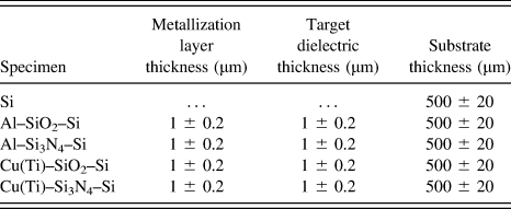
The preparation of the thin-films stacked specimen was carried out using the standard wafer fabrication process on a 100 mm-diameter wafer. The Si wafer was first going through a plasma-enhanced chemical vapor deposition process, where a homogenous layer of dielectric layer (SiO2 or Si3N4) was deposited on one side of the Si wafer surface. The Al or Cu metallization layer was then sputtered over the dielectric layer. However, a Ti layer of ∼50 nm was required prior to the Cu deposition for adhesion purpose. Lastly, the wafer was sawn mechanically into a 10 mm × 10 mm die size. Table I presents the geometrical information of the specimens used in this work.
Geometry specifications of the specimens.
III. RESULTS AND DISCUSSION
The indentation damage test was performed at the room temperature (25 °C) on five different specimens listed in Table I. A minimum of 20 indentation tests was conducted on the five different specimens, followed by a post-mortem analysis, examining both the planar and cross-section areas of the indentation region. The indented surface of the top metallization layer was usually removed by wet chemical etchant (i.e., mixture of acids) to expose the dielectric SiO2 or Si3N4 layer, and followed by rinsing the specimens with de-ionized water.Reference Yeo, Yong and Zhou41 This delayering failure analysis technique only revealed the bulk material cracking or damage on the surface of the dielectric layer. To examine for any interfacial crack or delamination within the stacked structure, the cross-sectioning approach using focused ion beam (FIB) and scanning electron microscopy (SEM) technique was used.
A. AE signal quality test
Ideally, a couplant medium (between the specimen and the AE sensor) should be easily applicable and removable from the sensor without affecting the loading process, while possessing excellent acoustic impedance, thus providing a good signal-to-noise ratio. Nail polish that consisted of a film-forming polymer dissolved in a volatile organic solvent was then used as a couplant medium.
It was found that the measurement of the Si die with and without the couplant medium was independent of the loading and unloading rate. Thus, Fig. 3 shows only the time and frequency responses of the first AE event occurrence at the 1 N/min load rate. Figure 3(a) shows that a clear distinct peak amplitude consistently occurred at ∼150 kHz for the Si die with couplant medium, but two different maximum amplitudes (∼150 and ∼200 kHz) occurred in the case without it [Figs. 3(b) and 3(c)]. The failure mode in the Si die was similar for both with and without the couplant medium, as shown in Fig. 4, where the ring crack and sometimes the radial crack were observed on the indented Si surface, and the subsurface cracking was also found in the Si from the FIB/SEM analysis.
Time and frequency responses of the first AE event occurrence for Si die: (a) with couplant medium, the maximum peak at ∼150 kHz, (b) without couplant medium, the maximum peak at ∼150 kHz, and (c) without couplant medium, the maximum peak at ∼200 kHz.
Failure modes of the Si die: (a) with and (b) without couplant medium.
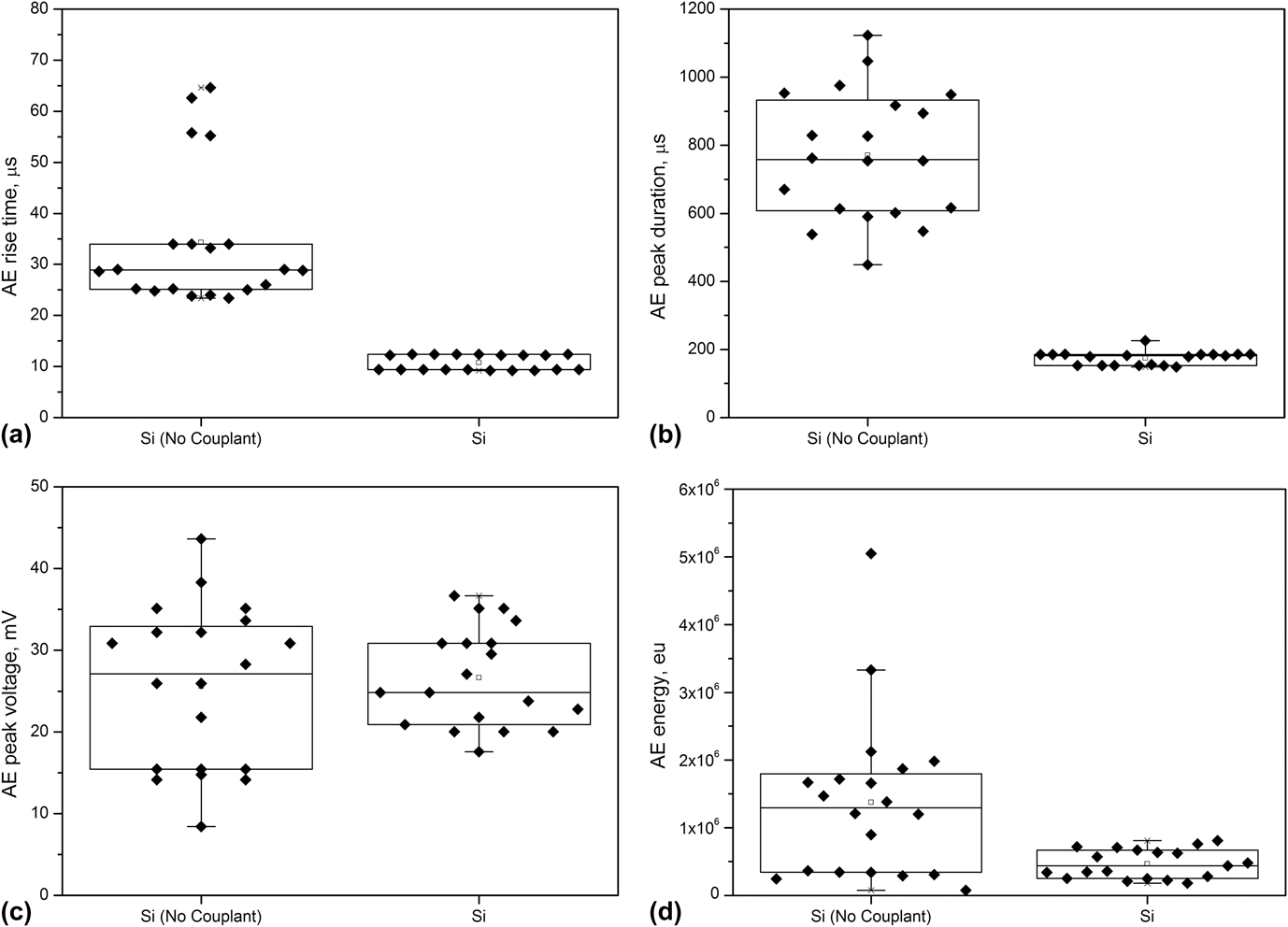
Different AE parameters are extracted and compared in Fig. 5. Generally, the introduction of nail polish as a couplant medium yielded a lower, consistent AE rise and duration. In additional, smaller standard deviations of the AE peak voltage and energy were also observed. It was found that a comparable mechanical response was measured for both Si dies with and without the couplant medium, which implies that the use of nail polish will not affect the mechanical result of the indentation.
AE signal results of the Si die with and without couplant medium: (a) rise time, (b) duration time, (c) peak voltage, and (d) energy.
Nail polish was applied in the subsequent damage test. Besides a good quality of AE signal detection, the specimen was able to adhere firmly on the AE sensor especially during the x–y–z motorized stage movement.
B. Damage test on the metal-coated stacked structure
The mechanical responses of the thin-films metal stacked specimens are presented in Fig. 6, together with the results of the Si die for comparison. The first AE event corresponded to the “pop-in” observation in the F–d curve shown in Fig. 6(a). This “pop-in” was a result of sudden increase in the distant traveled by the indenter when the cracking of the specimen occurred (for a load-controlled indentation) before reaching another resistance point. This suggests that the stored energy in the specimen converted from the work of indentation was released by fracture, and the specimen lost its structural integrity and stiffness at the instance of “pop-in” occurrence. A new stiffness would usually be measured after the “pop-in” if the indenter continued the loading process on the damaged specimen. However, in this test the indenter was retracted at the same rate as the loading process after the “pop-in” event.
Mechanical responses of the metal-coated thin-films stacked specimens: (a) indentation F–d response, and (b) onset crack forces at different loading rates.
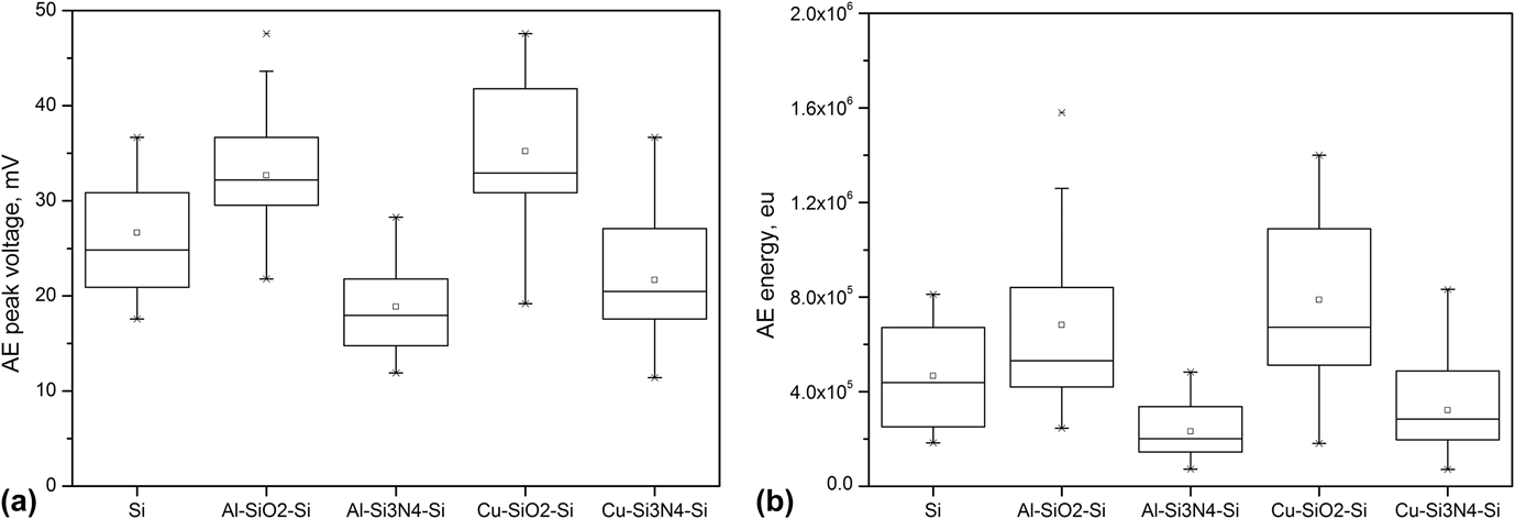
The mean onset crack forces measured were 1.2, 1.9, 2.0, 1.3, and 1.5 N for the Si, Al–SiO2–Si, Cu–SiO2–Si, Al–Si3N4–Si, and Cu–Si3N4–Si specimens respectively for different loading rates [Fig. 6(b)]. The results show that the measured onset crack forces were independent of the loading rate used in this indentation damage test. It was also observed that the onset crack forces strongly depended on the dielectric material used, as compared to the metallization layer. To validate the accuracy of the crack detection means by the AE sensor, all thin-films stacked specimens were tested at 1.1 N, a force closed to the minimum F cr of the Si die. There was no AE event detected and no damage was observed. In addition, this shows that the thin-films stacked layers enhanced the indentation damage threshold of the Si die. Generally, the specimens with SiO2 dielectric yielded a higher 1st AE peak voltage and energy [(Figs. 7(a) and 7(b)], which also corresponded to a higher onset crack force measured.
AE signal results of the Si die and various thin-films stacked specimens: (a) peak voltage, and (b) energy.
The AE time and frequency spectrum responses of the thin-films stacked specimens were quite similar, as compared to the Si die, where the maximum peak voltage of the 1st AE event usually occurred at ∼150 kHz [Figs. 3, 8 and 9]. However, it was found that a second AE event sometimes occurred during the unloading stage at 0.1–0.2 N, as shown in Figs. 8 and 9 for the cases of Al–SiO2–Si and Cu–SiO2–Si specimens, respectively. Both the first and second AE peak signals consistently occurred at 150 kHz, where the first peak voltage was always higher than the second one. Interestingly, there was no AE event detected during the unloading cycle for the case of bulk Si and metal-coated Si3N4 dielectric specimens.
Experiment results for Al–SiO2–Si specimen: (a) time history graph and F–d curve, time and frequency spectrum plots of (b) the first AE and (c) the second AE events.
Experiment results for Cu–SiO2–Si specimen: (a) time history graph and F–d curve, time and frequency spectrum plots of (b) the first AE and (c) the second AE events.
No cracking was observed in the top metallization layers for all the specimens after the indentation damage test, except for a round indented mark and a pile-up around the indented area. However, delayering of top metallization revealed peeling and radial cracking on the SiO2 surfaces, as shown in Figs. 10(a) and 10(c). Ring and radial cracking were observed on the Si3N4 surfaces for the Al metallization specimens [Fig. 10(b)], and only radial cracking was observed for the Cu metallization specimens [Fig. 10(d)]. This suggests that the softer Al experienced a larger pile-up during indentation, which could potentially induce a ring crack on the Si3N4 layer underneath, as compared to the Cu metallization with a Ti adhesive layer.
Surface optical images of the damaged specimens after indentation tests: (a) Al–SiO2–Si, (b) Al–Si3N4–Si, (c) Cu–SiO2–Si, and (d) Cu–Si3N4–Si.
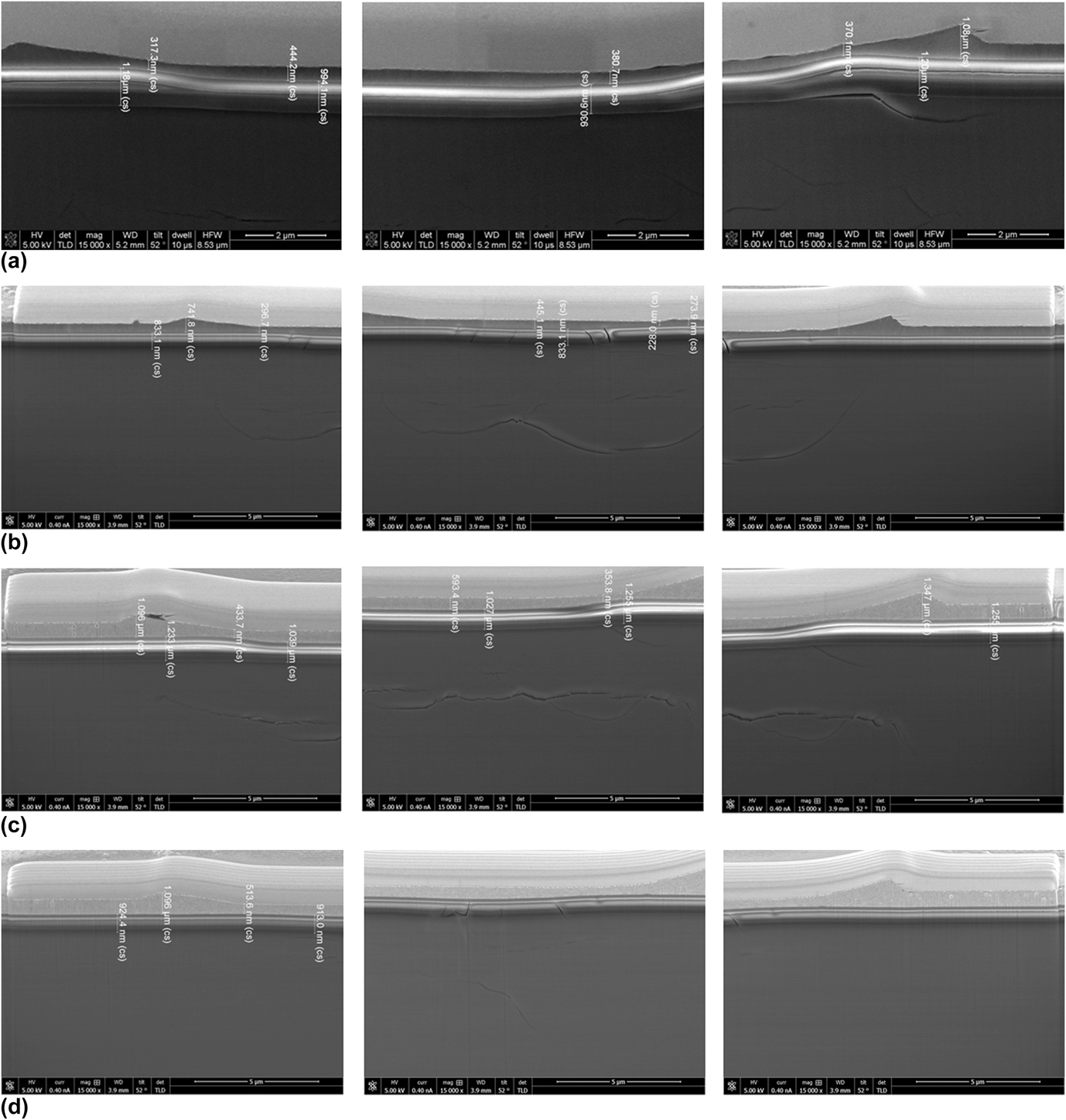
The cross-sectioning of the specimen was examined by FIB/SEM analysis, as presented in Fig. 11. The metal-coated SiO2 dielectric specimen demonstrated both the cone and subsurface cracking in the Si substrate [Figs. 11(a) and 11(c)], and delamination between the SiO2 and Si interface [Fig. 11(a)]. Furthermore, Figs. 10(a) and 10(c) show a partial “white-ring” at the perimeter of the imprinted SiO2 surface, which could be a tell-tale sign of dielectric peeling or delamination. However, for the metal-coated Si3N4 dielectric specimen, only subsurface cracking was found in the Si substrate, and through-thickness cracking was observed in the Si3N4 layer [Figs. 11(b) and 11(d)]. It was also observed that the damage on Si3N4 surface was severe especially for Al metallization specimen, where the ring and radial cracks were obvious with longer crack lines as compared to SiO2 [Fig. 10]. Hence, the delamination failure observed in the metal-coated SiO2 dielectric specimen could be related to the second AE event detected during unloading of the indenter.
Cross-sectioning images (FIB/SEM) of the damaged specimens after indentation tests: (a) Al–SiO2–Si, (b) Al–Si3N4–Si, (c) Cu–SiO2–Si, and (d) Cu–Si3N4–Si.
The SiO2 has an elastic modulus ∼5 times lower than Si3N4,Reference Madou42 and hence from the SEM cross-sectioned images [Fig. 11], the SiO2 dielectric layer experienced a larger deformation or “bending” without any through thickness cracking, as compared to the Si3N4 electric layer. This attested the lower onset crack force measured in the specimen with Si3N4 dielectric layer.
During the unloading stage, a larger elastic recovery of the metal-coated SiO2 dielectric specimen was expected, which could result in a large strain energy released through delamination or interfacial cracking between the dielectric layer and the Si substrate. Furthermore, the detected peak voltage of the first AE event was much larger than that of the second one, which could shed lights on the occurrence of different damage modes during the loading and unloading stages. A large ultrasonic wave intensity or AE energy was usually emitted for a sudden cracking as observed in the brittle dielectric layer or the Si substrate during loading stage, and a weak AE energy might account for the delamination failure during the unloading stage. In addition, this weak AE energy detected in the second AE event could be attenuated further at the damage areas (crack lines and gaps) induced during the earlier loading cycle.
There was no “pop-out” in the unloading F–d curve even when a second AE event was detected [Figs. 8(a) and 9(a)]. It was also reported elsewhere that the delamination does not usually lead to a “pop-out” in the F–d curves.Reference Chen and Bull32 However, Chang and Zhang reported the “pop-out” observation of the unloading F–d curve of the monocrystalline silicon using a Berkovich indenter. They described the “pop-out” as the result of different evolution processes of the phase transformations in the silicon, from Si-II to Si-III/Si-XII and/or to amorphous phases, thus reducing the volume of the residual Si-II zone.Reference Change and Zhang43
The damage test was then evaluated with a Vickers indenter, where 10 indentations were performed on the Si die. During the loading stage, the “pop-in” was not obvious in the F–d curve, where the average onset crack forces measured was ∼0.3 N corresponding to the first AE event detected. In the unloading stage, a “pop-out” in the F–d curve was observed, as shown in Fig. 12. However there was no AE event detected related to this “pop-out” occurrence, except the one near the end of the unloading stage, which could be related to the chipping of the Si. It is deduced that the AE sensor used in this damage test system is not capable of detecting any phase transformations in Si. It is also interesting to discover that the “pop-out” in the F–d curve only happened with a sharp tip indentation but not for a blunt tip, and this observation is still unclear and requires further work to be conducted.
Indentation F–d curve of the Si die using the Vickers indenter at the 1 N/min loading–unloading cycle, with the insert being the failure image of the indented Si surface.
C. Damage test on dielectric stacked structure after top metallization removal
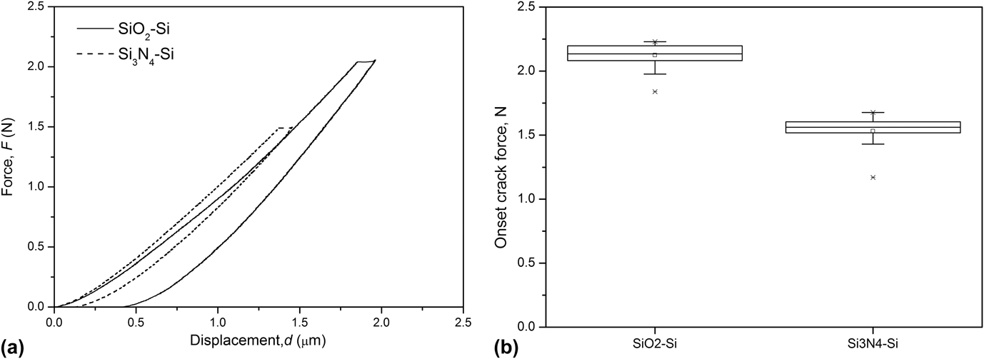
Additional test was evaluated on the specimens without the top metallization layer, with the aim to uncover the damage behavior during unloading. The top Al metallization was etched away to expose the dielectric layers. The loading and unloading rate of 1 N/min was used, and the results are presented in Fig. 13 with the mean onset crack force measured being ∼2.1 and ∼1.6 N for SiO2 and Si3N4 dielectric specimens, respectively. The results are slightly higher than those for the metal-coated specimens, which could be possibly explained by the different intrinsic or residue stress in the specimen before and after the removal of metallization. Nevertheless, this evaluation attests that the onset crack force is independent of the metal coating.
Mechanical responses of the dielectric layer specimens: (a) indentation F–d response, and (b) onset crack forces.
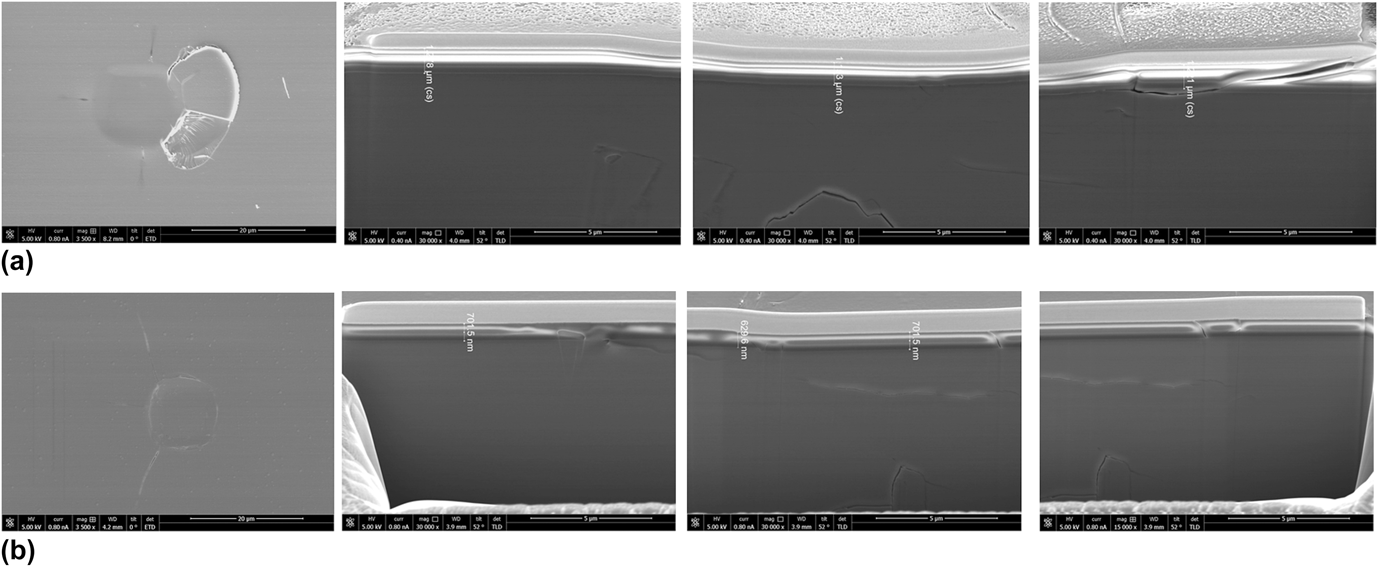
The radial cracking and chipping were observed on the SiO2 dielectric surface, and the cone and subsurface cracking was found in the Si substrate, as shown in Fig. 14(a). This is similar to the metal-coated SiO2 dielectric specimen, where chipping of the SiO2 layer could be due to the dielectric delamination during the unloading stage. The damage on the Si3N4 dielectric specimen is alike to that on the metal-coated Si3N4 dielectric specimen, where the radial, ring, and through-thickness cracking was observed in the Si3N4 dielectric, and the subsurface cracking was found in the Si substrate [Fig. 14(b)]
Cross-sectioning images (FIB/SEM) of the damaged specimens after indentation tests: (a) SiO2–Si, and (b) Si3N4–Si.
A 2nd AE event was detected during the unloading stage for the SiO2 dielectric specimen evaluated, which could be due to the delamination and chipping of the SiO2 layer. However, a few of the indentations on the Si3N4 dielectric specimens (<10%) also recorded a 2nd AE event, which is suspected to be the effect of the contact friction between the diamond indenter tip and the damaged and fragmented Si3N4 dielectric layer.
D. Indentation damage model of the metal-coated thin-films stacked structure
The damage behavior of the metal-coated thin-films stacked structure is presented in Fig. 15, and for illustration simplicity the pile-up effect of the top metallization is not drawn here. For the metal-coated SiO2 dielectric specimen [Fig. 15(a)], the top metallization underwent an elastic–plastic deformation during the loading (stage I), while the dielectric layer and the Si substrate were assumed to be deformed elastically. When the first AE event was detected, the loading stop (stage II) F cr was determined, which corresponded to the peeling and radical cracking on the dielectric surface, and the cone and subsurface cracking in the Si substrate. Immediately, the indenter proceeded to unload, and the stacked structure then underwent an elastic recovery. As the indentation load reduced, a second AE event occurred, which could result in the delamination or interfacial cracking in the dielectric layer and Si substrate (stage III). If the indentation damage test was performed on the exposed SiO2 dielectric specimen, chipping would occurred. While for the metal-coated Si3N4 dielectric specimen [Fig. 15(b)], the ring and radial cracking was observed on the dielectric surface, the cone and through-thickness cracking was observed in the dielectric layer, and the subsurface cracking was found in the Si substrate, when the first AE event was detected during the loading stage.
Indentation damage model for: (a) metal-coated SiO2 dielectric, and (b) metal-coated Si3N4 dielectric on Si substrate.
IV. SUMMARY
A damage test methodology invoking the techniques of instrumented indentation testing and AE sensing has been developed to evaluate the metal-coated thin-films stacked structure. The critical load F cr determined corresponds to the 1st AE event occurrence and the “pop-in” in the F–d curve, which is mainly due to the brittle cracking in the dielectric layer or Si substrate. A lower magnitude of a second AE event is detected, but no “pop-out” is observed in the F–d curve, which is related to delamination or interfacial cracking between the dielectric layer and the Si substrate. It is also found that “pop-out” during the unloading stage only happens with a sharp indenter tip and is related to the Si phase transformation, but not for a blunt indenter tip. In general, the onset crack force strongly depends on the dielectric layer used, as compared to the metallization layer. Furthermore, a higher onset crack force threshold is usually obtained in the metal-coated SiO2 dielectric specimen over the metal-coated Si3N4 dielectric specimen. Furthermore, delamination only happens in the metal-coated SiO2 dielectric specimen during the unloading stage.
This study provides an understanding of the indentation damage mechanisms of a soft metal coating over a brittle dielectric material structure. The application be found in the wire bonding process on the bond pad of an integrated circuit (IC) device, where the damage-sensitive pad can be identified and handled with care.Reference Yeo, Yong, Dan and Ruether40,Reference Yeo, Yong and Zhou41 Furthermore, the methodology can be implemented in terms of design rules or guidelines for the bond pad stack structure, or even as a mechanical screening tool for wafer quality check, which will eventually enable resilient statements for improving product quality and reliability of IC chips.
ACKNOWLEDGMENTS
The authors are grateful to the Failure Analysis colleagues from the Infineon Technologies Asia Pacific and the staff from Micro-machining Lab at Nanyang Technological University for their support in specimen preparation. The authors also acknowledge financial support from Ministry of Education, Singapore (Academic Research Fund TIER 1 - G128/14).