I. INTRODUCTION
Ever since Federal Communications Commission (FCC) announced unlicensed band from 3.1 to 10.6 GHz, research to develop components for ultra-wideband (UWB) systems has proliferated. One of the key components in the UWB system component design paradigm is a bandpass filter (BPF). A wide variety of BPF with numerous design techniques are reported in [Reference Hao and Hong1–Reference Saeid, Javad and Changiz10]. One of the important techniques is using a multimode resonator (MMR), which is highly preferable in designing a UWB BPF [Reference Hao and Hong1–Reference Wai and Lei3]. Fork form resonator is used to realize UWB passband, which is presented in [Reference Chen and Zhang4]. In [Reference Wang, Yang, Kang, Miao and Wu5] cross-shaped resonator and its application in UWB filter design domain is discussed. Many designs reported above basically cover the entire UWB range; however, the existing wireless local area Network (WLAN) (5.15 to 5.75 GHz) signals interfere with UWB devices. Hence, UWB BPF with notch band is highly desirable. Eliminating WLAN frequency a notch band in UWB passband is inserted as reported in [Reference Ali and Hu6–Reference Wadell12]. In [Reference Ali and Hu6], the notch characteristics are achieved by using meta-material complementary split ring resonator. Combining elliptic low-pass filter and distributed high-pass filter a UWB BPF is proposed in [Reference Ghatak, Sarkar, Mishra and Poddar7], where embedded stepped impedance resonator is realized to implement notch band. In [Reference Wen-Jeng, Jian-Yi, Lih-Shan, Ding-Bing and Mau-Phon8], open circuited metal lines embedded in defected ground structure is reported for notch implementation. Asymmetric coupled feed line can also be used to obtain notch characteristics [Reference Chan Ho and Kai9].
In this paper, a UWB BPF is proposed by using MMR constructed by loading an open-ended stub and an asymmetric step impedance stub in a uniform impedance resonator. A single notch band is implemented by using a spiral resonator at 5.25 GHz. Rest of the paper is organized as follows. The T-shaped resonator-based wideband BPF design procedure and analysis is presented in Section 2. Section 3 deals with analysis of changes in resonance characteristics due to loading of asymmetric stub on the T-shaped resonator analyzed in Section 2. This is followed by Section 4 where a spiral resonator is embedded in the proposed UWB BPF to introduce notch. Concluding remarks is given in Section 5.
II. DESIGN AND CHARACTERIZATION OF OPEN STUB-LOADED UNIFORM IMPEDANCE RESONATOR (UIR)
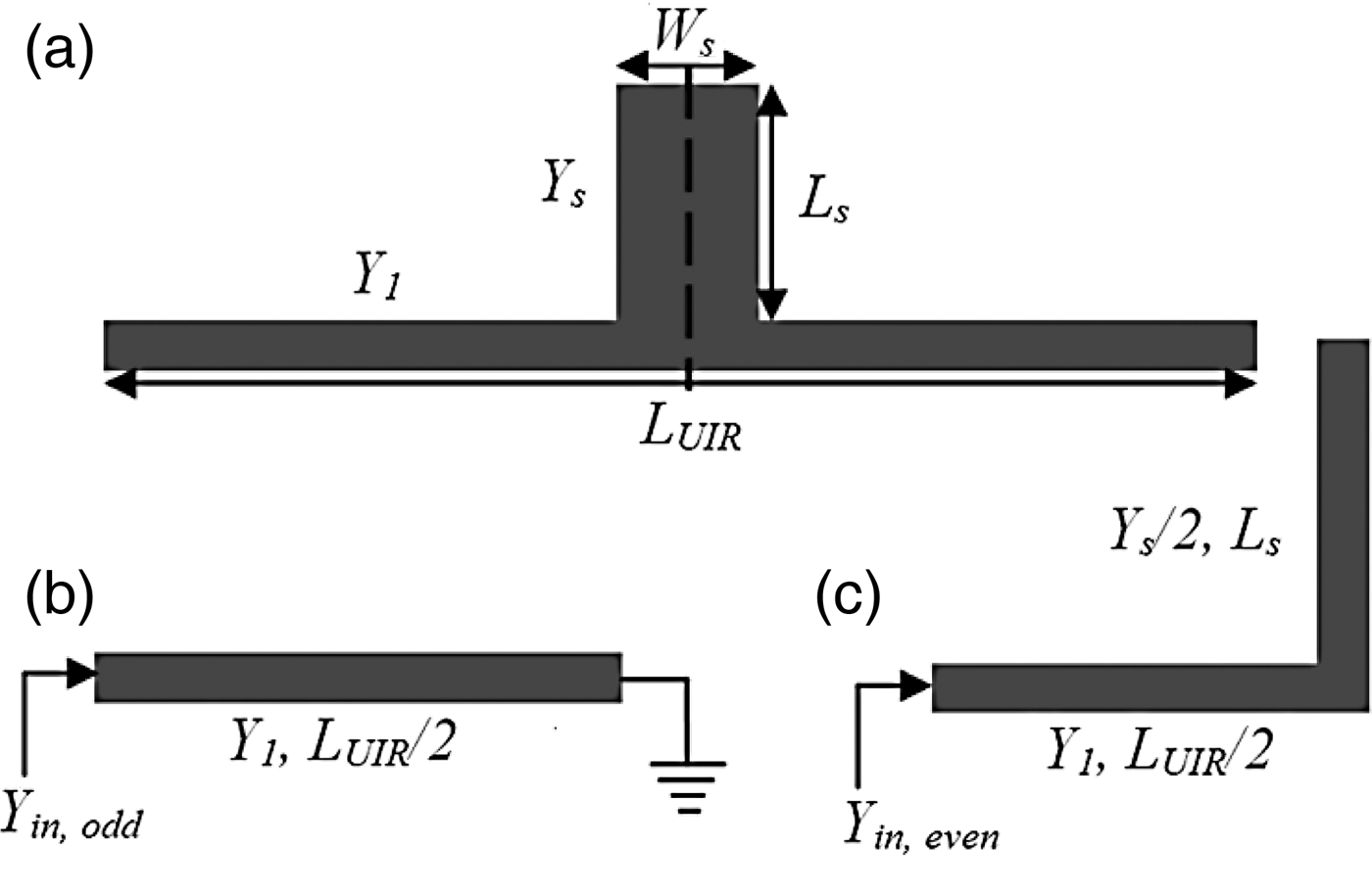
The initial design is an open stub-loaded UIR with input/output coupling as indicated in Fig. 1. This forms a stub-loaded resonator, which is shown in Fig. 2. The stub loaded resonator (SLR) is analyzed using even- and odd-mode techniques. The parameters pertaining to a stub-loaded resonator are illustrated in Fig. 2(a) with Figs 2(b) and 2(c) denoting the even- and odd-mode equivalent circuits after bifurcating the resonator along the line of symmetry denoted in Fig. 2(a).
Layout of a typical stub-loaded T-shape resonator with L S = 3.05, L 1 = 8.55, L UIR = 20, W S = 1.0, W 1 = 0.3, W = 0.2, g = 0.1, L g = 8.65, and W g = 1.2 (all dimensions are in mm).

(a) Structure of the proposed stub-loaded resonator, (b) odd-mode equivalent circuit, and (c) even-mode equivalent circuit.
The odd-mode equivalent circuit of Fig. 2(b) due to the voltage null along the middle of the T-shape resonator, offers an input admittance Y in,odd.
 $$Y_{in\comma odd}=\displaystyle{{Y_1 } \over {j\tan \left({{{\theta _1 } / 2}} \right)}}.$$
In (1), θ1 = βL UIR is the electric length of the microstrip line. From the resonance condition of Y in, odd = 0, the odd-mode resonant frequencies can be deduced as
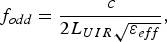 $$f_{odd}=\displaystyle{c \over {2L_{UIR} \sqrt {\varepsilon _{eff} } }}\comma \;$$
where n = 1, 2, 3, … and c is the speed of light in the free space, and εeff denotes the effective dielectric constant of the substrate. For design simplicity n = 1 is taken.
The open stub does not affect the odd-mode resonant frequencies.
For even mode of stub-loaded resonator, the input admittance of the equivalent circuit of Fig. 2(c) is approximated as
 $$Y_{in\comma even}=jY_1 \displaystyle{{\tan \left({{{\theta _1 } / 2}} \right)+Y_S \tan \left({\theta _S } \right)} \over {2Y_1 - Y_2 \tan \left({{{\theta _1 } / 2}} \right)\tan \left({\theta _S } \right)}}\comma \;$$
where θS = β× L S is the electric length of the open stub.
Applying the resonance condition, at even-mode resonant frequencies,
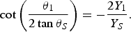 $$\cot \left({\displaystyle{{\theta _1 } \over {2\tan \theta _S }}} \right)=- \displaystyle{{2Y_1 } \over {Y_S }}.$$
For design simplicity, Y S = 2Y 1 is considered. Therefore, (4) reduces to that in (5).
 $$\cot \left({{{\theta _1 } / 2}} \right)\tan \left({\theta _S } \right)=- 1.$$
Therefore, the even-mode resonance condition is
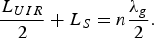 $$\displaystyle{{L_{UIR} } \over 2}+L_S=n\displaystyle{{\lambda _g } \over 2}.$$
The even-mode resonant frequencies can be written as
 $$f_{even}=\displaystyle{{nc} \over {\lpar L_{UIR}+2L_S \rpar \sqrt {\varepsilon _{eff} } }}.$$
Using (2)–(7) the length “L UIR” is computed to be 20 mm corresponding to λg/2 at fundamental odd-mode resonant frequency of 5.6 GHz. The resonator is realized on a substrate of εr = 2.2 and height 0.787 mm. For all electromagnetic (EM) simulations in this work, commercially available software CST Microwave StudioTM is used. Parametric variation of open stub dimensions and its effect on resonance characteristics is given in Figs 3(a) and 3(b), respectively. If L S increases the even-mode resonance frequency shift to lower frequency but the odd-mode resonant frequency is not affected. From variation in even-mode resonance as depicted in Fig. 3(b) it can be inferred that (7) predicts changes in odd-mode resonance frequency with change in length of open stub “L S”. However, it fails to predict the change in even-mode resonance for changing width of stub. The variation of width of stub brings about a change in effective length of L UIR/2 by an amount ±ΔW S/2. The positive sign indicates a decrease in stub impedance and negative sign is for increase in stub impedance. This leads to modifications of even-mode resonance condition (6) and even-mode frequency (7) resulting in (8) and (9), respectively.
Effect on resonance characteristics on varying, (a) stub length (L S) and (b) the stub width (W S) for weak coupling of the open stub-loaded resonator.
 $$\displaystyle{{L_{UIR} } \over 2} \pm \displaystyle{{\Delta W_S } \over 2}+L_S=n\displaystyle{{\lambda _g } \over 2}\comma \;$$
 $$f_{even}=\displaystyle{{nc} \over {\left({L_{UIR} \pm \Delta W_S+2L_S } \right)\sqrt {\varepsilon _{eff} } }}.$$
The length and width of open stub that load the UIR need to be fine-tuned as it influences even- and odd-mode resonance frequency and hence the passband behaviors of the proposed bandpass filter (BPF). The variation of S 11 (dB) for change in L S and W S are given in Figs 4 (a) and 4(b), respectively. From this parametric study a fine-tuned value of L S is found to be 3.05 mm and that for W S it is 1.0 mm. In the input–output (I/O) coupling is realized by 50 Ω tap line with interdigital coupled line. However, to enhance the coupling of I/O port section, two ground slots are used as shown in Fig. 1. The resonance characteristic of the weakly coupled optimum T-shaped resonator is shown in Fig. 5 which indicates resonance at 5.6 and 8.8 GHz, respectively. Revisiting Figs 4(a) and 4(b), it can be observed that the passband obtained for the stub-loaded resonator extends from 4 to 10 GHz, which is wide but not enough to cover the UWB range. This confirms to the observation reported in [Reference Kaixue, Liang, Jayasuriya and Seng11] where the stub-loaded resonator is used to design wideband BPF. In the ensuing section, the stub-loaded resonator is modified to achieve the desired UWB passband bandwidth.
S-parameters plot for parametric study of (a) stub length (L S) and (b) the stub width (Ws) under strong coupling of structure as shown in Fig 1.
Resonant characteristic of a T-shape resonator under weakly coupled condition.
III. LOADING OF STUB-LOADED RESONATOR WITH OPEN-ENDED ASYMMETRIC STEPPED IMPEDANCE STUB (ASIS)
A folded open-ended ASIS is used to load the stub-loaded resonator as shown in Fig. 6. The ASIS is quarter wavelength long at 3.25 GHz, which is also confirmed from weakly coupled EM analysis of the composite double stub-loaded resonator as shown in Fig. 7. The composite structure thus provides three resonating frequency at 3.25, 5.6, and 8.8 GHz. These three modes eventually merge to give the UWB passband. To gain an insight in to the resonance behavior a transmission line network model of the double stub-loaded resonator is developed as shown as inset in Fig. 7. The net ABCD matrix of the model is derived to analyze the composite resonator system. The overall ABCD matrix of the resonator is the product of five ABCD matrices as given in (10) corresponding to the model illustrated in inset of Fig. 7.
Layout of the proposed UWB filter using an ASIS with L 1ASIS = 7.3, W 1ASIS = 0.2, L 2ASIS = 7, W 2ASIS = 2.75, L 1UIR = 10.0, L 2UIR = 1.05, and L 3UIR = 8.95 (all dimensions are in mm).
Resonating modes of UIR loaded with two open-ended stubs. Transmission line model of composite resonator is shown an inset.
 $$\eqalign{& \left[{\matrix{ {A_T } & {B_T } \cr {C_T } & {D_T } \cr } } \right]=\left[{\matrix{ A & B \cr C & D \cr } } \right]_{UIR}^1 \times \left[{\matrix{ A & B \cr C & D \cr } } \right]_S \times \left[{\matrix{ A & B \cr C & D \cr } } \right]_{UIR}^2 \cr & \quad\quad\quad\qquad \times \left[{\matrix{ A & B \cr C & D \cr } } \right]_{ASIS} \times \left[{\matrix{ A & B \cr C & D \cr } } \right]_{UIR}^3 .}$$
In (10), the ABCD matrix of a transmission line, which models the UIR sections, and that of open shunt stub is given below in (11) and (12), respectively [Reference Kaixue, Liang, Jayasuriya and Seng11, Reference Wadell12].
 $$\left[{\matrix{ A & B \cr C & D \cr } } \right]_{UIR}=\left[{\matrix{ {\cos \theta } & {jZ_0 \sin \theta } \cr {jY_0 \sin \theta } & {\cos \theta } \cr } } \right]\comma \;$$
 $$\left[{\matrix{ A & B \cr C & D \cr } } \right]_S=\left[{\matrix{ 1 & 0 \cr {jY_S \tan \theta _S } & 1 \cr } } \right].$$
The ABCD matrix of the ASIS appears as an admittance, which is given as
 $$\left[{\matrix{ A & B \cr C & D \cr } } \right]_{ASIS}=\left[{\matrix{ 1 & 0 \cr {Y_{in}^{ASIS} } & 1 \cr } } \right].$$
The input admittance of the ASIS is derived as given in (14)
 $$Y_{in}^{ASIS}=- jY_{ASIS}^1 \displaystyle{{Z_{ASIS}^1 \tan \theta _{ASIS2}^2+Z_{ASIS2}^2 \tan \theta _{ASIS1}^1 } \over {Z_{ASIS1}^1 \tan \theta _{ASIS1}^1 \tan \theta _{ASIS2}^2 - Z_{ASIS2}^2 }}.$$
The frequency response of the ASIS loaded resonator under strong coupling is shown in Fig. 8. This modified MMR has more degree of design freedom and provides better selectivity. The UWB filter has a circuit size of 20.5 mm × 6.5 mm. By tuning the electrical length ratio and impedance ratio of ASIS the lower transmission zero at 2.62 GHz is achieved. The other transmission zero at 13 GHz is due to source load coupling. The ASIS is designed such that the optimum Z 1ASIS and Z 2ASIS are 157.84 and 45.89 Ω, respectively [Reference Chan Ho and Kai13]. The corresponding electrical lengths θ1ASIS and θ2ASIS are 37.23° and 37.70° at 3.25 GHz.
EM simulated S-parameters of the proposed UWB BPF.
IV. EMBEDDING A SPIRAL RESONATOR WITH UWB BPF
A UWB BPF with passband from 3.04 to 10.8 GHz is designed and described in Sections 2 and 3. In addition to the wide passband, it is desirable that the filter can mitigate interference from WLAN frequencies. For this a spiral resonator [Reference Marta, Jordi and Ferras14] is embedded in the filter topology as shown in Fig. 9. The spiral resonator is design at 5.25 GHz to stop WLAN interference. The spacings between coupled line and spiral resonator is tuned to achieve satisfactory attenuation at the desired WLAN frequency. The photograph of the fabricated UWB BPF is shown in Fig. 10. The S-parameters of the proposed filter are measured using Rhode and Schwarz ZVA40 vector network analyzer. Fig. 11 depicts the simulated and measured S-parameters that are in close agreement. Lower cutoff is obtained at 3.04 GHz whereas higher cutoff is at 10.8 GHz for S 11 dB better than 10 dB. Measured fractional bandwidth is about 125%. Over the desired band the insertion loss is <1.5 dB. The measured transmission zeros are at 2.59 and 13.0 GHz, respectively, that contribute in enhancing the passband selectivity. At the notch frequency of 5.25 GHz, the measured insertion loss is more than 15 dB. The group delay is also plotted in Fig. 11, which indicates distortion less transmission. However, at the notch frequency 5.25 GHz the group delays fluctuates drastically.
(a) Layout of a UWB BPFs with single notch band. (b) The spiral resonator with L 1SR = 0.75, L 2SR = 1.60, L 3SR = 0.9, L 4SR = 1.50, L 5SR = 2.75, L 6SR = 1.55, L 7SR = 3.30, L 8SR = 1.50, L 9SR = 1.40, L 10SR = 3.30, W SR = 0.20, and s = 0.15 (all dimensions are in mm).
Photograph of fabricated prototype of the proposed band-notched UWB BPF.
Comparison of S-parameters obtained from EM simulation and measurement. Also shown is the group delay profile of the BPF.
V. CONCLUSION
In this paper, a compact UWB BPF using an MMR realized by loading an open-ended short stub and open-ended ASIS in uniform impedance half wavelength resonator. Design steps of gradually achieving UWB passband is explained in detail. The notch band at 5.25 GHz is introduced by embedding a spiral resonator. The UWB band ranges from 3.04 to 10.8 GHz for S 11 better than 10 dB. Measured transmission zero is achieved at 2.59 and 13 GHz and stop band till 15 GHz is obtained. The insertion loss within the passband is below 1.5 dB. The prototype is fabricated and measured which agrees well with the simulated response. Owing to compact size (20.5 mm × 6.5 mm) and excellent in band and out of band characteristics the filter can be used in the UWB system.
ACKNOWLEDGEMENTS
Rowdra Ghatak, Manimala Pal, Ishita Rakshit, and Sharmili Adhikari are grateful to Department of Science and Technology, Government of India, for supporting their research under DST-FIST grant to ECE Department, NIT Durgapur vide sanction no. SR/FST/ETI-267/2012(c) Dated 10th June 2011.
 Pankaj Sarkar received his M.Tech. Degree from the University of Burdwan in 2009. He worked 1 year in Space Applications Center – Ahmedabad as a trainee for M. Tech. project entitled as “Design of MMIC Mixer at 50–60 GHz”. He initiated his teaching carrier from ITER (Siksha “O” Anusandhan University – Bhubaneswar), after that he served Sikkim Manipal Institute of Technology and National Institute of Technology – Sikkim. Presently he is Assistant Professor in Electronics and Communication Engineering Department of North-Eastern Hill University – Shillong. He has more than 20 publications in various National/International journals and conferences. His research interest lies in the area of microwave passive circuit design, metamaterials, MMIC, and antenna. Currently, he is pursuing Ph.D. from Jadavpur University.
 Ishita Rakshit received her B. Tech. Degree in Electronics and Communication Engineering from National Institute of Technology Durgapur in 2013. She has been one of the top ten finalists in the Electromagnetic Olympiad held by IEEE AP/MTT chapter Kolkata section. Her area of interest is in microwave circuit design, high-power radio frequency source design, and soft computing technique.
Sharmili Adhikari received her B. Tech. Degree in Electronics and Communication Engineering from National Institute of Technology Durgapur in 2013. She is a gold medalist in her undergraduate curriculum. She has received DAAD fellowship “WISE” in 2012 and worked in top institutes at Germany. She has also received numerous scholarships from various organizations. Her area of interest is in microwave circuit design and semiconductor electronics.
Manimala Pal received her M.Tech. (Microwave Engineering) Degree from the University of Burdwan in 2010. She started her research on microwave circuits at Radionics Laboratory. Presently she holds a faculty position in Electronics and Communication Engineering Department, Faculty of Engineering and Technology of NSHM Knowledge Campus, Durgapur, West Bengal. Her areas of interest lie in design and optimization of planar bandpass filters and couplers, UWB antenna and development of tools for microwave engineering education. She has more than forty publications in various International and National journal as well as conferences. She is a member of microwave and antenna research group at NIT Durgapur as external fellow. She is a member of IEEE and has been actively engaged in organizing workshops in microwave engineering.
 Rowdra Ghatak received his M.Tech. (Microwave Engineering) Degree from The University of Burdwan and Ph.D. (Engg) from Jadavpur University in 2002 and 2008, respectively. Presently he is a professor in Electronics and Communication Engineering Department of National Institute of Technology Durgapur. He is a recipient of the URSI Young Scientist Award in 2005. He has recently received support under DST Young Scientist scheme for development of UWB antennas for imaging RADAR. He has more than 100 publications in various National/International journals and conferences. His research interest lies in the areas of fractal antenna, metamaterial, application of evolutionary algorithms to electromagnetic optimization problems, RFID, computational electromagnetic, and microwave passive circuit design. He is a reviewer of IEEE, IET, Elsevier, JEMWA, Journal from Brazilian microwave Association, John Wiley, and PIER journals. He is a member of IEEE and has organized workshops in the capacity of workshop chair/convener on Microwave Circuits and Antenna.