Introduction
In order to meet the ever-stringent demands of emerging wireless-communication systems, RF microwave components with various enhanced functionalities are always desired. Among them, a plurality of research activities aimed at developing balanced/differential-mode bandpass filters (BPFs) with multi-band bandpass transfer functions are recently attracting considerable attention [Reference Martin, Zhu, Hong and Medina1]. Such RF multi-band pre-selection devices are expected to be required by modern multi-standard/multi-purpose highly-integrated RF front-end chains. This is because they are more robust than their single-ended counterparts to undesired common-mode noise and electromagnetic (EM)-interference/crosstalk effects that may arise between the different layers in ultra-compact/highly-miniaturized RF transceivers as on-going RF system-level design trend.
When compared to balanced single-band BPFs, it becomes more difficult to design differential-mode dual- or multi-band BPFs with satisfactory common-mode-rejection performance. In order to achieve high common-mode suppression levels within the differential-mode passbands, balanced dual-/multi-band BPFs using different design techniques have been reported in the technical literature as in [Reference Shi and Xue2–Reference Gómez-García, Muñoz-Ferreras, Feng and Psychogiou11]. They mostly consist of coupled-resonator filter configurations that are properly modified to attain the differential-mode dual-passband filtering behavior while simultaneously suppressing the in-band common-mode RF signal. For example, by exploiting asymmetrical or symmetrical open-ended stubs loaded at the filter symmetry plane, balanced dual-band BPFs using coupled stepped-impedance resonators (SIRs) [Reference Shi and Xue2], doubly short-ended coupled lines [Reference Yang, Choi, Tam and Zhu3], SIR ring resonators [Reference Ren, Liu, Ma, Ohira, Wen, Wang and Guan4], and stub-loaded shunted-line resonators [Reference Ren, Guan, Liu, Ma and Ohira5] were studied. In [Reference Cho and Yun6], balanced dual-band BPFs with asymmetrical SIR-based coupled lines were developed. Subsequently, by using four U-shaped slotline resonators etched at the ground plane, a type of compact balanced dual-band BPF using coupled-embedded SIR resonators was presented in [Reference Bagci, Fernández-Prieto, Lujambio, Martel, Bernal and Medina7]. In yet another approach, by making use of the intrinsic common-mode-rejection property of balanced microstrip-to-slotline transitions, differential-mode multi-band and dual-band BPFs realized in four-port balanced topologies were discussed in [Reference Zhang, Qiu and Chu8] and [Reference Wei, Yu, Zhang, Zeng and Shi9], respectively. Moreover, based on a four-port wideband balanced branch-line structure loaded with two pairs of multiple short-circuit-ended stubs, a class of differential-mode planar multi-band BPFs was engineered in [Reference Gómez-García, Loeches-Sánchez, Psychogiou and Peroulis10]. Similarly, balanced dual-band BPFs with symmetrical quasi-reflectionless behavior can also be developed, as it was corroborated in [Reference Gómez-García, Muñoz-Ferreras, Feng and Psychogiou11]. However, most of the aforementioned balanced dual-/multi-band BPF architectures suffer from some drawbacks, such as relatively-poor selectivity around the differential-mode passbands, among some others.
On the other hand, transversal-signal-interference RF passive filters have emerged in the last few years as a suitable alternative to coupled-resonator circuit networks for single/multi-band BPF design using non-conventional multi-path filtering structures [Reference Gómez-García, Sánchez-Renedo, Jarry, Lintignat and Barelaud12–Reference Mirzaee and Virdee17]. Examples of their employed constituent transversal filtering sections include bi-path in-parallel-transmission-line-based cells and directional power couplers and dividers with loaded stubs, which are arranged in transversal mode. In this manner, from the frequency-dependent constructive/destructive interference phenomena at the output node among the multiple signal components in which the input signal is divided to produce passbands/stopbands, single/multi-band BPFs with ultra-sharp rejection capabilities can be generated. Nevertheless, due to their intrinsic frequency-periodic behavior in most cases, and more especially for multi-band BPFs, they suffer from narrow stopband bandwidths [Reference Gómez-García, Muñoz-Ferreras and Sánchez-Renedo15]. Whereas the exploitation of stepped-impedance-line paths in transversal signal-interference dual-band BPFs has been recently proposed in [Reference Gómez-García and Yang18] as an effective technique to partially circumvent this limitation, the problem still remains at the lower stopband. Furthermore, it should be remarked upon that most of these transversal-signal-interference filters are of the single-ended type, with just a very few cases of differential-mode multi-band BPFs that heritage the referred drawback from their single-ended precursors as the one simulated in [Reference Loeches-Sánchez, Psychogiou, Gómez-García and Peroulis19] that lacks from experimental demonstration.
In this paper, as an extension of the preliminary work from the authors in [Reference Yang, Malki, Fan and Gómez-García20] for the single-ended case, an original type of balanced quasi-elliptic-type dual-band BPFs is developed. In differential-mode operation, they exploit as basic building block a two-path coupled-line-based transversal filtering section in which a second-order sharp-rejection dual-band BPF response with several close-to-passband transmission zeros (TZs) at both passband sides is obtained. When compared to their transversal single-ended and balanced dual-band BPF precursors without coupled-line stages in their circuit networks, enlarged stopband bandwidths are attained. Furthermore, by properly adjusting the line-impedance values of the open-ended stubs that are loaded at the filter symmetry plane, high common-mode rejection levels within the differential-mode passbands can be achieved through in-band common-mode multi-TZ generation. Higher-order realizations composed of in-series cascade connections of several replicas of the balanced dual-band BPF stage are also feasible, as theoretically verified with a fourth-order two-stage design example. In addition, the discrete-time modeling of the reported balanced dual-band BPFs is also presented toward a better understanding of its zero/pole characteristics. Note that although this framework was previously applied to single-ended transversal-signal-interference and coupled-line filters in [Reference Muñoz-Ferreras and Gómez-García21] and [Reference Muñoz-Ferreras, Psychogiou and Gómez-García22], respectively, this is the first time that this modeling technique is extended to differential-mode RF filters, hence allowing to “mimic” their behavior from a digital perspective. Finally, for experimental-demonstration purposes, a 1.464/2.294 GHz proof-of-concept microstrip prototype of the designed two-stage/fourth-order differential-mode dual-band BPF example is manufactured and characterized.
Design, analysis, and digital modeling
This section presents the RF operational principles of the proposed transversal-signal-interference coupled-line-based balanced dual-band BPF. First, the theoretical foundations of its constituent second-order differential-mode dual-band BPF stage and design guidelines based on parametric-circuit analysis are reported. Subsequently, the feasibility of higher-order in-series-cascaded multi-stage designs to attain increased differential-mode selectivity and higher in-band common-mode suppression levels is demonstrated in a two-stage/fourth-order balanced dual-band BPF realization. Finally, as a further original contribution of this work related with the modeling of balanced dual-band BPFs in the digital domain – which is demonstrated here by the very first time for balanced RF filters – the discrete-time representation of single-stage/second-order and two-stage/fourth-order theoretical design examples is addressed.
Second-order balanced dual-band BPF
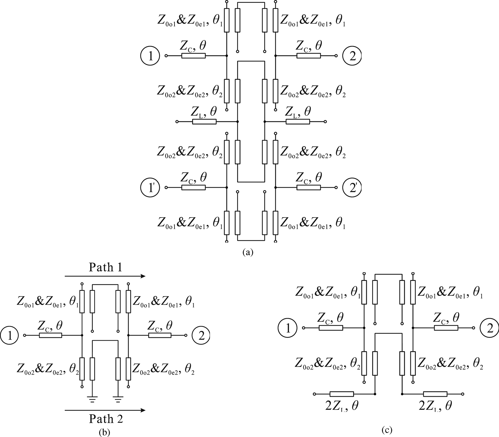
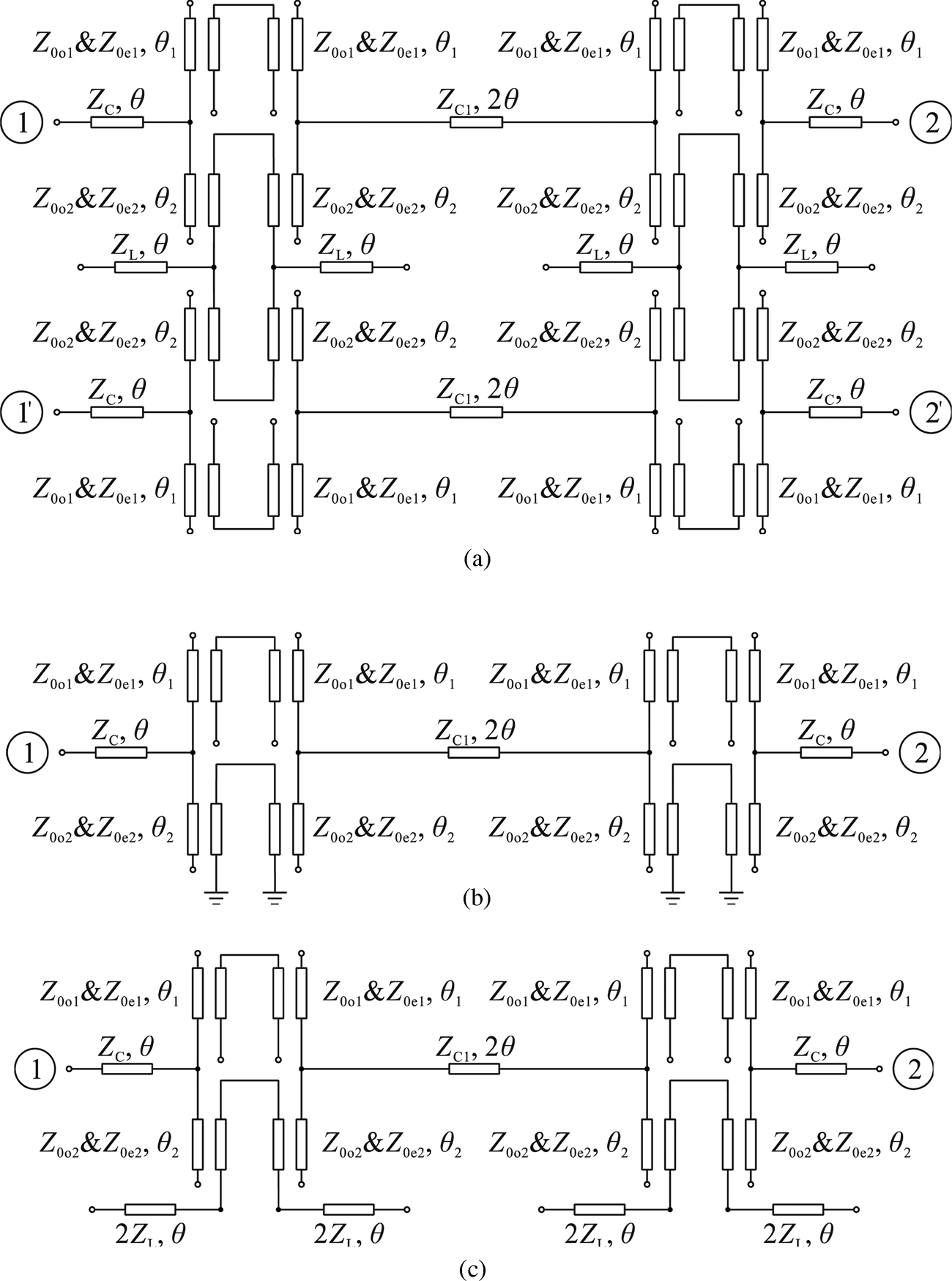
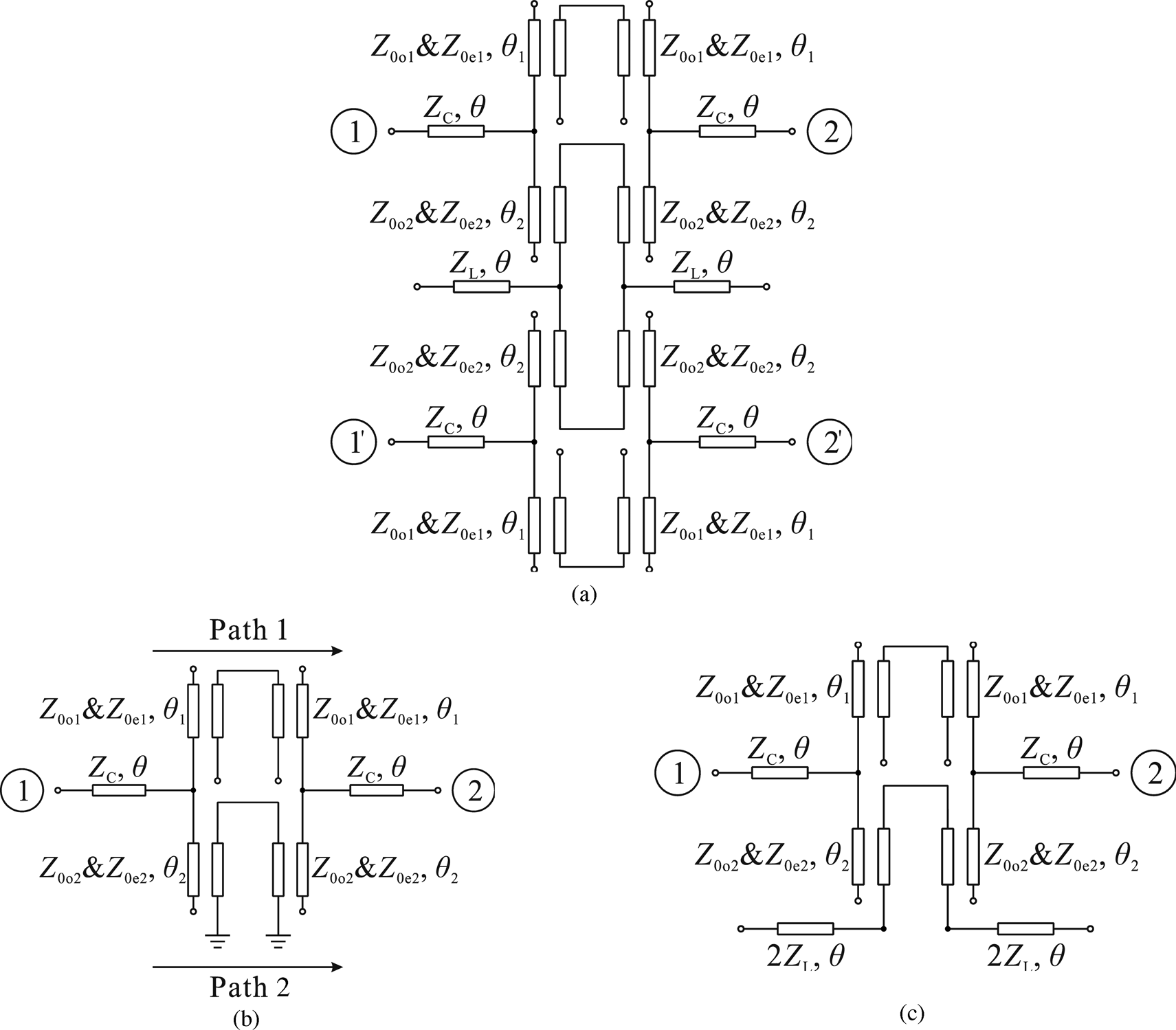
The equivalent circuit of the proposed second-order balanced dual-band BPF stage with indication of its design parameters is depicted in Fig. 1(a). The properties of this balanced circuit are determined by means of its associated two-port differential- and common-mode equivalent sub-circuits, respectively. When the differential-mode RF signals are excited at the pairs of input (Ports 1 and 1′) and output (Ports 2 and 2′) ports, a virtual electrical wall is produced at the symmetry plane of the balanced BPF architecture. As illustrated in Fig. 1(b), its two-port differential-mode equivalent sub-circuit is derived, in which all the circuit points that are connected to the symmetry plane become virtually short ended. Here, the open- and short-ended half-wavelength resonators are in-parallel coupled with the input and output T-junctions. In this manner, based on these four constituent coupled-line sections in the engineered two-path transversal-signal-interference section, a second-order dual-band BPF filtering response with sharp-rejection selectivity can be obtained. At the same time, the other two quarter-wavelength line segments are utilized to improve the in-band power-matching levels of the two designed passbands. On the other hand, Fig. 1(c) depicts the two-port common-mode equivalent sub-circuit of this second-order balanced BPF. A magnetic wall is then created at the symmetry plane when a common-mode excitation is applied to the pairs of input and output ports, which results in the impedance value of the loaded open-ended stubs to be doubled as 2ZL.
Equivalent circuits of the proposed second-order balanced dual-band BPF based on a transversal-signal-interference coupled-line section. (a) Four-port balanced network with circuit detail (ZC, ZL, Z 0o1, Z 0e1, Z 0o2, and Z 0e2 correspond to characteristic-, odd-mode-, and even-mode-impedance variables of the in-series input/output connecting lines, the shunt open-ended stubs that are loaded at the symmetry plane, and the two relevant coupled-line sections, respectively, whereas the electrical lengths θ, θ 1, and θ 2 correspond to line segments that are quarter-wavelength long at the design frequency f 0 or θ(f 0) = θ 1(f 0) = θ 2(f 0) = 90°. (b) Two-port differential-mode equivalent sub-circuit. (c) Two-port common-mode equivalent sub-circuit.
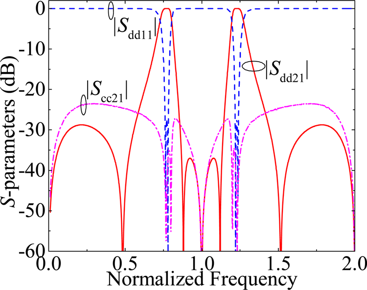
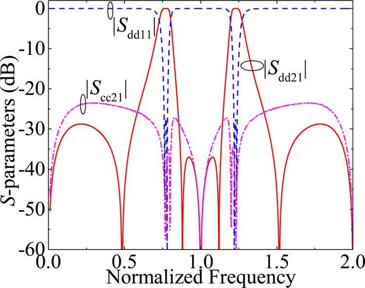
To verify the above descriptions for the proposed second-order balanced dual-band BPF, its theoretical frequency responses based on the relevant even- and odd-mode theoretical analysis of the two-port differential- and common-mode equivalent sub-circuits can be determined. Due to their mathematical complexity, these formulas have been omitted here. Various illustrative responses based on parametric-circuit analysis are provided instead as more useful information for the designer. Specifically, in Fig. 2, the theoretical power transmission and reflection responses for a design example of second-order balanced dual-band BPF under differential- and common-mode operation are presented. As can be seen, two sharp-rejection passbands with several close-to-passband TZs at their both sides are attained for the differential mode, which are spectrally symmetrical with regard to the inter-passband TZ produced at the design frequency f 0. Furthermore, by means of the selected values for the impedance-line design parameters (ZC, Z 0o1, Z 0e1, Z 0o2, Z 0e2, and ZL), common-mode power-rejection levels above 23.5 dB for the proposed second-order balanced BPF are attained through the generation of several common-mode multi-TZ creation within the spectral period [0, 2f 0]. Note that the TZs at DC and 2f 0 are due to the fact of not having direct signal-transmission path (i.e. without coupled-line stages) between the input and output terminals for both the differential- and common-mode equivalent sub-networks in Fig. 1(b) and 1(c), respectively. The TZ at f 0 is produced by the quarter-wavelength-at-f 0 open-ended stubs of the coupled-line stages connected to the input/output ZC-impedance lines. The remaining TZs are caused by the transversal interaction among the two signal-propagation paths, so that the two signal components propagated by them inter-cancel out at the output node for these frequencies to produce signal transmission nulls.
Theoretical differential-mode power transmission (|Sdd 21|), reflection (|Sdd 11|), and common-mode suppression (|Scc 21|) responses of the proposed second-order balanced dual-band BPF in Fig. 1(a) with ZC = 42 Ω, Z 0e1 = 77.5 Ω, Z 0o1 = 31.8 Ω, Z 0e2 = 98.7 Ω, Z 0o2 = 32.5 Ω, ZL = 16.7 Ω, and θ(f 0) = θ 1(f 0) = θ 2(f 0) = 90° (reference impedance Z 0 = 50 Ω).
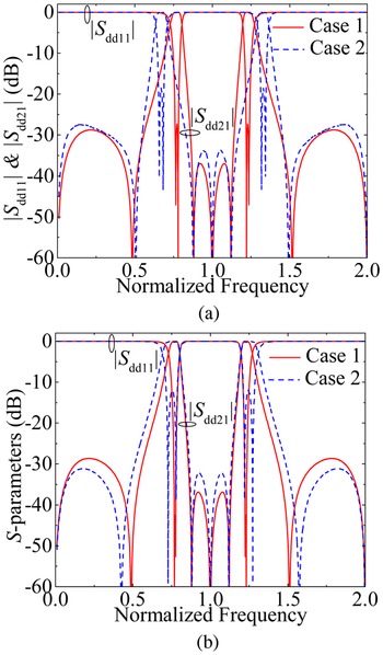
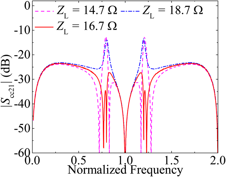
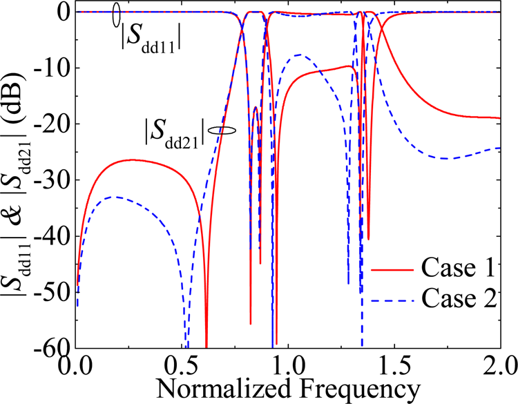
To further demonstrate the design flexibility of the proposed second-order differential-mode dual-band BPF stage in Fig. 1(b) in differential-mode operation, several frequency responses with flexible dual passbands are discussed for two situations, as follows: (i) constant absolute bandwidths but different center frequencies and (ii) different absolute bandwidths but fixed TZs at the inter-passband region. Specifically, as observed in Fig. 3(a) for the selected set of values of the design impedances, quasi-elliptic-type dual passbands with constant absolute bandwidth of 77 MHz for each passband at the center frequencies of 0.7655f 0 and 1.2345f 0 (case 1) and 0.6715f 0 and 1.3285f 0 in (case 2), respectively, are realized. Additionally, the two passbands can be also designed with different bandwidths, but with fixed TZs at the frequency interval between these two passbands. As depicted in Fig. 3(b), the bandwidths of the dual passbands are enlarged from case 1 to case 2, where the TZs for the first passband at its left-hand side and for the second passband at the right-band side are shifted to lower and upper frequency locations, respectively, as a result of the referred bandwidth increase. In both cases, the two passbands are spectrally symmetrical with regard to the design frequency f 0. In addition, the common-mode power-rejection performance of the second-order balanced BPF versus different values of ZL is also discussed. As depicted in Fig. 4, the common-mode suppression levels at the out-of-band spectral regions remain almost unchanged as ZL is varied, whereas the power rejection levels within the frequency ranges of the differential-mode dual passbands are more sensitive to the employed low impedance ZL. These results reveal that the value of ZL should be properly chosen for the selected values of the line-impedance parameters of the differential-mode equivalent sub-circuit, which is vital to functionalize high common-mode suppression levels within the differential-mode dual passbands by means of common-mode multi-TZ creation. Consequently, the careful adjustment of the geometrical parameter associated to the impedance ZL during the practical EM simulation becomes critical to attain high in-band common-mode rejection levels.
Theoretical frequency responses of the second-order differential-mode equivalent circuit in Fig. 1(b) associated to the proposed second-order balanced dual-band BPF. (a) Power transmission (|Sdd 21|) and reflection (|Sdd 11|) responses for differential-mode dual passbands with constant absolute bandwidth but with different center frequencies versus different values of the design impedances (Case 1: ZC = 42 Ω, Z 0e1 = 77.5 Ω, Z 0o1 = 31.8 Ω, Z 0e2 = 98.7 Ω, and Z 0o2 = 32.5 Ω; Case 2: ZC = 20.4 Ω, Z 0e1 = 79.4 Ω, Z 0o1 = 24.9 Ω, Z 0e2 = 117.23 Ω, and Z 0o2 = 30.74 Ω). (b) Power transmission (|Sdd 21|) and reflection (|Sdd 11|) responses for differential-mode dual passbands with different bandwidths versus different values of the design impedances (Case 1: ZC = 42 Ω, Z 0e1 = 77.73 Ω, Z 0o1 = 31.78 Ω, Z 0e2 = 98.59 Ω, and Z 0o2 = 32.6 Ω; Case 2: ZC = 33 Ω, Z 0e1 = 76.49 Ω, Z 0o1 = 32.22 Ω, Z 0e2 = 100.73 Ω, and Z 0o2 = 31.03 Ω).

Theoretical common-mode suppression (|Scc 21|) responses of the corresponding sub-circuit in Fig. 1(c) associated to the proposed second-order balanced dual-band BPF versus different values of ZL when ZC = 42 Ω, Z 0e1 = 77.5 Ω, Z 0o1 = 31.8 Ω, Z 0e2 = 98.7 Ω, and Z 0o2 = 32.5 Ω.

Finally, note that further flexibility may be attained by designing the coupled-line stages of the transversal filtering section as non-quarter-wavelength segments (i.e. θ 1(f 0), θ 2(f 0) ≠ 90°). In such case, spectrally-asymmetrical dual-band filtering transfer functions can be realized. This is demonstrated in Fig. 5, where two examples of differential-mode dual-passband responses with static in-band performance for the first passband and different bandwidth and center frequency for the second passband for each case are shown. Note that these two responses exhibit strong spectral asymmetry in terms of bandwidths and power-rejection profiles at their both sides, for which the design parameters of the transversal filtering section need to be properly adjusted. Nevertheless, more-complex common-mode suppression networks may be needed to attain high common-mode suppression levels in these situations, possibly involving the use of stepped-impedance-line segments and/or even more stubs connected at the symmetry plane of the overall circuit in Fig. 1(a).
Theoretical power transmission (|Sdd 21|) and reflection (|Sdd 11|) responses of the second-order differential-mode equivalent circuit in Fig. 1(b) for dual passbands with different bandwidths and out-of-band rejection profiles (Case 1: ZC = 42 Ω, Z 0e1 = 77.73 Ω, Z 0o1 = 31.78 Ω, Z 0e2 = 98.59 Ω, Z 0o2 = 32.6 Ω, θ 1(f 0) = 77°, and θ 2(f 0) = 84.5°; Case 2: ZC = 26.3 Ω, Z 0e1 = 76.27 Ω, Z 0o1 = 32.72 Ω, Z 0e2 = 84.8 Ω, Z 0o2 = 32.82 Ω, θ 1(f 0) = 79°, and θ 2(f 0) = 85°).

Fourth-order balanced dual-band BPF
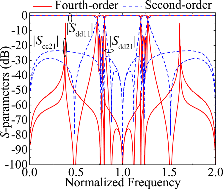
By exploiting the previously-proposed second-order balanced dual-band BPF as basic building block, its fourth-order balanced dual-band BPF counterpart can be developed. Such higher-order design is expected to show enhanced differential-mode passband selectivity and stopband power-attenuation levels, as well as increased in-band common-mode suppression levels. As depicted in Fig. 6(a), a fourth-order balanced dual-band BPF can be directly designed through two in-series-cascaded transversal coupled-line-based balanced dual-band BPF stages as the one detailed in Fig. 1. They are connected by means of half-wavelength-at-f 0 (i.e. electrical length 2θ(f 0) = 180°) line segments with characteristic impedance ZC 1. Consequently, the two-port differential- and common-mode equivalent sub-circuits of this proposed high-order balanced dual-band BPF topology are the ones provided in Fig. 6(b) and 6(c), respectively, which are derived under applying the corresponding excitation at the pairs of input and output ports of the overall filter. To demonstrate the expected properties of this fourth-order balanced dual-band BPF architecture, its frequency responses compared with the ones of its constituent second-order balanced dual-band BPF in Fig. 1 are depicted in Fig. 7. As can be seen, highly-increased dual-passband filtering selectivity and augmented stopband power-rejection levels are attained with the selected values for the design impedances. Although two undesired spurious narrow-band peaks appear at the lower and upper stopband frequency regions under both differential- and common-mode excitations, they are attributed to the inter-stage cascading process as it was carefully analyzed in [Reference Morini, Venanzoni, Martín-Iglesias, Ernst, Sidiropoulus, Donato and Farina23]. Furthermore, when compared to its building second-order balanced dual-band BPF stage, highly-enhanced common-mode power-suppression levels of this fourth-order balanced dual-band BPF design are obtained within the interval [0.5f 0, 1.5f 0], which covers the operating frequency region of the differential-mode dual passbands. Note finally that this multi-stage in-series-cascaded design approach can be extended to any number of replicas for even higher-order balanced dual-band BPF realizations.
Equivalent circuits of the proposed fourth-order balanced dual-band BPF based on the connection of two replicas of the in-series cascaded second-order balanced transversal coupled-line-based dual-band BPF units in Fig. 1 through half-wavelength microstrip lines. (a) Four-port balanced dual-band BPF network. (b) Two-port differential-mode equivalent sub-circuit. (c) Two-port common-mode equivalent sub-circuit.

Theoretical differential-mode power transmission (|Sdd 21|), reflection (|Sdd 11|), and common-mode suppression (|Scc 21|) responses of the proposed fourth-order balanced dual-band BPF in Fig. 6 with ZC = 42 Ω, ZC 1 = 50 Ω, Z 0e1 = 77.5 Ω, Z 0o1 = 31.8 Ω, Z 0e2 = 98.7 Ω, Z 0o2 = 32.5 Ω, and ZL = 16.7 Ω.

Digital modeling
As it can be seen in the theoretical design examples in Fig. 7, the ideally-synthesized power transmission responses of the proposed balanced dual-band BPFs are frequency periodic of period 2f 0 for both the differential and common modes. This fact leads to the possibility of modeling these circuits as discrete-time linear time-invariant systems with a frequency response being periodic of period 2π rad/sample. Despite such framework was initially proposed in [Reference Muñoz-Ferreras and Gómez-García21] for signal-interference filters and extended to coupled-line filters in [Reference Muñoz-Ferreras, Psychogiou and Gómez-García22] of the single-ended type, its application to balanced/differential-mode RF filters has never been addressed. However, its conceptual interest is remarkable to properly understand the theoretical foundations of such balanced dual-band BPFs from a digital perspective, as well as to obtain discrete-time models for them which may be useful for their digital emulation. Thus, by applying this modeling method to frequency-periodic RF circuits containing coupled-line sections as the balanced dual-band BPFs of this work, the real-valued coefficients ak (k = 0, 1, …, N) and bk (k = 0, 1, …, M) of the transfer function of the digital system in the complex-valued variable z associated to the transmission scattering parameter of both the differential and common modes can be extracted.
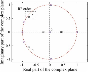
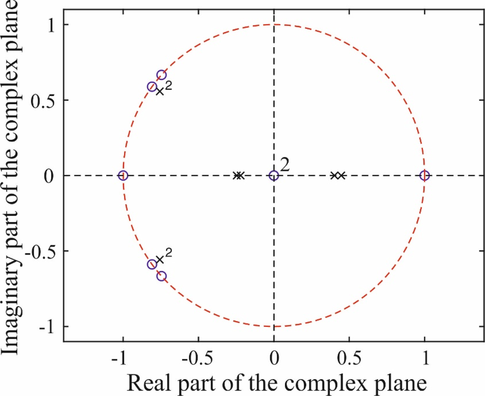
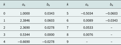
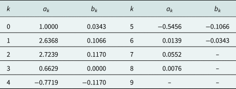
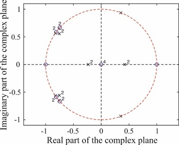
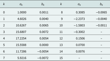
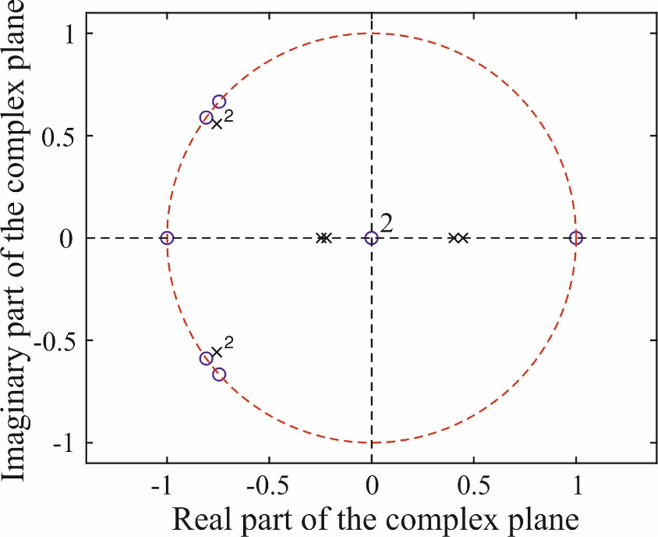
As verification of the referred digital modeling, the coefficients ak and bk corresponding to the ideal design of the one-stage balanced dual-band BPF in Fig. 7 for the differential and common modes are listed in Tables 1 and 2, respectively. As observed, one interesting feature is that both sets of coefficients have identical orders M = 6 and N = 8 for both the differential and common modes. The zero-pole diagrams in the z-plane associated to the differential- and common-mode transmission scattering parameters for the one-stage circuit are drawn in Figs. 8 and 9, respectively. Due to the passivity property of the circuit, the poles appear contained within the unit circumference. Moreover, the TZs are those located on the unit circumference. Finally, the two poles near the unit circumference in the second and third quadrants of the complex plane in Fig. 8 permit to explain the number of reflection zeros for each passband of the differential-mode power transmission parameter for this one-stage balanced dual-band BPF circuit (see Fig. 7).
Zero-pole diagram of the digital system associated to the differential-mode transmission scattering parameter of the one-stage balanced dual-band BPF in Fig. 7 (poles are represented with black symbol “x”; zeros are represented with blue symbol “o”; numbers indicate the multiplicity of the root).

Zero-pole diagram of the digital system associated to the common-mode transmission scattering parameter of the one-stage balanced dual-band TFS in Fig. 7 (poles are represented with black symbol “x”; zeros are represented with blue symbol “o”; numbers indicate the multiplicity of the root).
Coefficients ak and bk of the digital model associated to the differential-mode power transmission response of the one-stage balanced dual-band BPF in Fig. 7

Coefficients ak and bk of the digital model associated to the common-mode power transmission response of the one-stage balanced dual-band BPF in Fig. 7

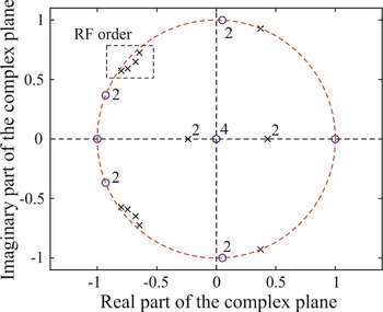
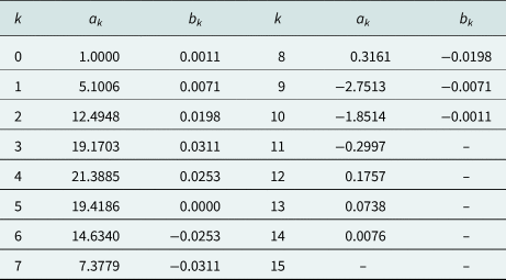
The coefficients ak and bk corresponding to the ideal design of the two-stage balanced dual-band BPF in Fig. 7 for the differential and common modes are respectively listed in Tables 3 and 4, whereas the associated zero-pole diagrams are depicted in Figs. 10 and 11, respectively. As can be seen, the polynomial orders are increased to M = 10 and N = 14, thus confirming the enhanced selectivity attained for the differential-mode passbands and the increased common-mode rejection levels for this two-stage design when compared to the one-stage balanced dual-band BPF. On the other hand, the number of poles near the unit circumference in the second and third quadrants of the complex plane in Fig. 10 are increased to four, which correctly matches with the observed number of reflection zeros for each passband of the differential-mode power transmission parameter for the two-stage balanced dual-band BPF design (see Fig. 7).
Zero-pole diagram of the digital system associated to the differential-mode transmission scattering parameter of the two-stage balanced dual-band BPF in Fig. 7 (poles are represented with black symbol “x”; zeros are represented with blue symbol “o”; numbers indicate the multiplicity of the root).

Zero-pole diagram of the digital system associated to the common-mode transmission scattering parameter of the two-stage balanced dual-band BPF in Fig. 7 (poles are represented with black symbol “x”; zeros are represented with blue symbol “o”; numbers indicate the multiplicity of the root).

Coefficients ak and bk of the digital model associated to the differential-mode power transmission response of the two-stage balanced dual-band BPF in Fig. 7

Coefficients ak and bk of the digital model associated to the common-mode power transmission response of the two-stage balanced dual-band BPF in Fig. 7

Implementation and measurement
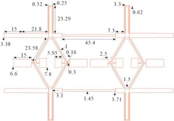
To experimentally validate the high-order differential- and common-mode frequency responses in Fig. 7 (i.e. the selected design-parameter values were taken as starting point of the layout-level design process), a planar fourth-order balanced dual-band BPF prototype is simulated and manufactured in microstrip technology. A Rogers 4003C substrate with relative dielectric constant εr = 3.55, dielectric thickness h = 1.524 mm, metal thickness t = 35 μm, and dielectric loss tangent tan(δD) = 0.0027 is employed for its fabrication. Figure 12 depicts the layout of the proposed fourth-order balanced BPF. As it was previously discussed, in order to achieve high in-band common-mode power-rejection levels for the proposed second-order balanced dual-band BPF, low-impedance lines being loaded at the symmetry plane of the circuit are employed. However, considering the large line widths of the low-impedance microstrip lines, a low-impedance microstrip line connected by a section of high-impedance microstrip line, which results in an SIR-type structure, is utilized in the practical EM simulation of the proposed fourth-order balanced dual-band BPF. Specifically, in order to attain high in-band common-mode suppression levels, two pairs of the suggested SIR-type microstrip lines with different lengths are loaded at the filter symmetry plane as it can be visualized in the layout in Fig. 12. Note also that a fine optimization of the overall circuit was needed after the inclusion of such SIR-type stubs to obtain the expected results in terms of differential-mode sharp-rejection dual-passband filtering response with in-band common-mode suppression.
Layout of the implemented fourth-order balanced dual-band BPF based on its relevant four-port equivalent circuit in Fig. 6 (all the indicated physical dimensions are given in mm).

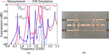
The EM-simulated and measured results of the manufactured fourth-order balanced dual-band BPF prototype, along with its photograph, are depicted in Fig. 13. The proposed fourth-order dual-band BPF is initially designed with center frequencies of 1.45 GHz and 2.3 GHz, respectively. As shown in Fig. 13(a), a fairly-close agreement between the EM-simulated and measured results is attained. The measured differential-mode BPF features two quasi-elliptic-type sharp-rejection passbands with enhanced stopband-power-attenuation levels. On the other hand, for the EM simulated and measured common-mode suppression, the presence of some unexpected spurious narrow-band spikes at the spectral region between two differential-mode passbands is observed. Their origin is associated with the adopted physical layout for the filter prototype, mostly with the coupled-line-based sections that are connected by microstrip lines in small physical dimensions and the loaded SIR-type microstrip lines at the filter symmetry plane.
Manufactured fourth-order balanced dual-band BPF prototype with its layout in Fig. 11. (a) Simulated and measured differential-mode power transmission (|Sdd 21|), reflection (|Sdd 11|), and common-mode suppression (|Scc 21|) responses. (b) Photograph.

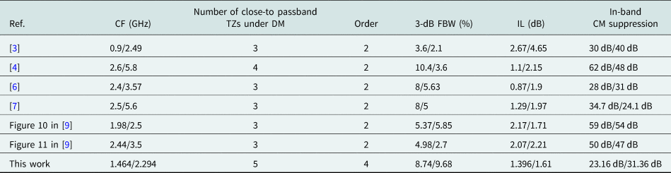
The main measured performance metrics of this engineered fourth-order differential-mode dual-band BPF for the lower and upper differential-mode passbands, respectively, are as follows: center frequencies of 1.464 GHz and 2.294 GHz, minimum in-band insertion-loss levels of 1.396 dB and 1.61 dB, minimum in-band return-loss levels of 14.13 dB and 15.86 dB, and 3-dB fractional bandwidths of 8.74% and 9.68%, respectively. In addition, the measured in-band common-mode rejection levels are higher than 23.16 dB and 31.36 dB for the measured balanced dual-band BPF. Furthermore, a performance comparison of the devised fourth-order balanced BPF prototype with other related prior-art balanced dual-band BPFs is given in Table 5. As can be seen, the fourth-order differential-mode dual-band BPF in this work features the highest order for the differential-mode passbands that provides it very-sharp-rejection capabilities, the highest number of TZs, and the widest fractional bandwidth for the second passband along with competitive in-band insertion loss. Furthermore, it is the only one exploiting the transversal-signal-interference filtering formalism, exhibiting in-band common-mode suppression levels that are comparable to those of some other previously-published related designs, such as those in [Reference Cho and Yun6] and [Reference Bagci, Fernández-Prieto, Lujambio, Martel, Bernal and Medina7].
Comparison with other prior-art balanced dual-band BPFs

CF, center frequency; DM, differential mode; FBW, fractional bandwidth; IL, insertion loss; CM, common mode.
Conclusion
A class of planar balanced transversal coupled-line-based dual-band BPFs with quasi-elliptic-type response has been reported. Based on the proposed second-order balanced dual-band BPF stage, its operational characteristics under differential- and common-mode excitations are detailed. To further improve the differential-mode passband selectivity and stopband attenuation levels of the second-order balanced dual-band BPF stage, as well as the in-band common-mode suppression levels, in-series-cascaded multi-stage designs particularized in a two-stage/fourth-order realization have been illustrated. Finally, a fourth-order balanced dual-band BPF microstrip prototype is designed, simulated, and characterized to validate the design concept. Although common-mode spurious peaks appear at the spectral region between the differential-mode dual passbands, very-sharp-rejection differential-mode passbands with TZs are measured, along with acceptable in-band common-mode suppression levels. As an additional contribution of this work, the digital modeling of these types of balanced dual-band BPFs has been shown, this being the first time it is applied to differential-mode RF filters.
Acknowledgements
This work was supported in part by the GOT ENERGY TALENT (GET) fellowship program cofunded by the EU as part of the H2020-MSCA-COFUND program under Grant Agreement number 754382 and in part by the Spanish Ministry of Economy, Industry, and Competitiveness (State Research Agency) under Project PID2020-116983RB-I00.
 Li Yang received the M.Sc. degree in electrical and electronics engineering and the Ph.D. degree in electrical and computer engineering from the University of Macau (UM), Macau, China, in 2013 and 2018, respectively. In 2018, he was a Research Associate with the Department of Electrical and Computer Engineering, UM. Since 2018, he holds a post-doctoral position with the Department of Signal Theory and Communications, University of Alcalá, Alcalá de Henares, Spain, where he is currently a GOT ENERGY TALENT (GET)-COFUND Marie Curie Fellow. His current research interests include the synthesis and design of RF/microwave planar and multilayered passive filters, reconfigurable filters, filtering antennas, and multifunctional circuits and systems. Dr. Yang was a recipient of the Best Student Paper Award of the International Symposium on Antennas and Propagation 2010 in Macau.
 Mohamed Malki received the B.Sc. degree in telecommunication engineering from the University of Alcalá, Madrid, Spain, in 2020. He is currently pursuing the M.S. degree in telecommunication engineering, in the specialized area of Space and Defense Technologies at the University of Alcalá, Madrid, Spain. Since 2022, he joined the Department of Signal Theory and Communications at the University of Alcalá, Alcalá de Henares, Madrid, Spain, as a Research Assistant. His main research interests include the analysis, design, and construction of microwave filters and multiplexers.
 José-María Muñoz-Ferreras received the degree in telecommunication engineering and the Ph.D. degree in electrical and electronic engineering from the Polytechnic University of Madrid, Spain, in 2004 and 2008, respectively. He is currently an Associate Professor with the Department of Signal Theory and Communications, University of Alcalá, Alcalá de Henares, Spain. His current research interests include radar signal processing, advanced radar systems and concepts, and microwave/RF circuits and systems, specifically focusing on high-resolution inverse synthetic aperture radar images, and the design and validation of radar systems for short-range applications. Dr. Muñoz-Ferreras is a member of the IEEE MTT-S Biological Effects and Medical Applications (MTT-28) Technical Committee and a reviewer for several IEEE and IET publications. He serves as a member of the Technical Review Board of the IEEE International Geoscience and Remote Sensing Symposium, the IEEE Radar Conference, the European Radar Conference, and the IEEE MTT-S International Microwave Symposium.
 Roberto Gómez-García is a Full Professor with the Department of Signal Theory and Communications, University of Alcalá, Alcalá de Henares, Spain. His current research interests include the design of fixed/tunable high-frequency filters and multiplexers in planar, hybrid, and monolithic microwave-integrated circuit technologies, multifunction circuits and systems, and software-defined radio and radar architectures for telecommunications, remote sensing, and biomedical applications. In these topics, he has authored/co-authored about 125 papers in international journals and 165 papers in international conferences. He was a recipient of the 2016 IEEE Microwave Theory and Techniques Society (MTT-S) Outstanding Young Engineer Award. He is an IEEE Circuits and Systems Society Distinguished Lecturer (2020–2022). Besides, he is the Editor-in-Chief of IEEE Microwave and Wireless Components Letters (2022–2024). He has served and currently serves as Associate/Guest/Senior Editor for several IEEE, IET, and EuMA journals. He is also a member of several Technical Committees within MTT-S and CAS-S.