Introduction
The field of antenna has faced a myriad of challenges in the past decade and has led to the evolution of different design techniques with the Theory of Characteristics Mode (TCM) providing a breakthrough in designing the antenna [Reference Chen and Wang1–Reference Harrington and Mautz3]. On the other hand, in today's scenario, it is the hour of the need for faster wireless communication transmitting and receiving data. The above two discussions have emerged as the implementation of TCM in designing multiple-input-multiple-outputm×n (MIMOm×n) antennas without applying input signal. The MIMO configuration of the antenna designed for multiple applications ensures a higher data rate, lower multiple path fading, and keeping intact the operating bandwidth. Several structural studies have been reported by the method of characteristics of mode analysis enabling applications in personal digital assistants (PDAs), personal area network (PAN) which include multiple applications such as hand-held radios, bluetooth speakers and a very new IoT technology enabled Alexa [Reference Mohanty and Behera4]. A three-mode analysis applied to patch and ground provides resonance at 2.55, 4.70, 7.50 and 2.50 GHz, 4.60 and 7.00 GHz respectively. This also suggests a wider impedance bandwidth of 2.00–9.50 GHz [Reference Zhao, Yeo and Ong5]. In [Reference Lau, Manteuffel, Arai and Hum6], the study shows that very less exploration has been done until 2015 were very few papers were published using TCM, and therefore, the analysis of modern antenna provides more potential. The CMA analysis has also been implemented on uni-feed antenna analyzing broad impedance bandwidth and axial-ratio (AR) bandwidth [Reference Chen, Li, Qi, Zhu and Zhao7]. Also, a connected cross-stub in the ground is analyzed by using 12 modes which shows the significance of the stub in-ground providing higher isolation [Reference Singh and Tripathi8]. In an electrically small antenna, using meandered stub shows the impedance which directs the flow of current at mode-1 and mode-2 with mode-1 more prominent showing resonance at 2.50 GHz [Reference Sohrabi, Dashti and Ahmadi-Shokouh9]. 6-mode analysis shows multiple resonances for planar inverted-F antenna making it useful for lower band applications at 3.50 and 4.30 GHz [Reference Kumar and Khanna10]. The compensation of mutual interference in the MIMO antenna is analyzed by physically placing the array elements at 0.50λ between them [Reference Lou and Wang11]. Prediction of Eigen modal currents and respective modal patterns at 2.45/5.80 GHz shows the distribution of current for both resonating frequencies and hence, thereby resulting in required corresponding radiation patterns [Reference Mohanty and Behera12–Reference Mohanty and Sahu14]. For the high frequency 5G MIMO antenna working at 27.40–28.50 GHz bandwidth, only mode-1 has modal significance while mode-2 has no role to play [Reference Abdelaziz and Hamad15]. A MIMO antenna utilizing meta-material cells offers resonance at 5.80 GHz with the value of modal significance to 1 at 5.80 GHz [Reference Jabire, Zheng, Abdu and Song16–Reference Mohanty and Behera18]. A circularly polarized antenna is subjected to 6-modes analysis with mode-1, mode-3, mode-4, mode-5 and mode-6 are interest of relevance between 3.00—and 15.0 GHz and finds applications in C- and X-bands [Reference Jaiverdhan, Sharma, Yadav and Dhara19–Reference Perli and Rao22]. A 2 × 2 MIMO antenna with reconfigurable capability occupies the overall size of 24 × 48 mm2 and a MIMO antenna with fractal radiating patch offers −10 dB impedance bandwidth of 2.84–15.88 GHz [Reference Hadda, Sharma, Gupta, Kumar and Singh23, Reference Sharma, Vashist, Alsukayti, Goyal, Anand and Mosavi24]. A cylindrical DRA MIMO configuration supports a dual orthogonal hybrid mode with an operating narrow bandwidth 2.40–3.88 GHz and a 24 × 48 mm2 2-port MIMO antenna with commonly connected CPW-ground provides isolation of more than 15 dB between the two radiators [Reference Bharti, Kumar, Gautam and Sharma25, Reference Jaiverdhan, Sharma and Yadav26]. High rejection triple notched band UWB-X band is achieved on high permittivity dielectric substrate with permittivity 11.2 [Reference Sharma, Awasthi and Singh27]. CMA analysis is carried out by using 7-modes which achieves n77/n78/n79 bands [Reference Addepalli, Babu, Beno, Potti, Nageshwara, Sundari and Devana28], and assymetrical Calendula-shape radiating patch also exhibits of achieveing three bands [Reference Addepalii, Vidyavathi, Neelima, Sharma and Kumar29]. The modal analysis is applied to sloteed anteena [Reference Babu, Aldhaheri, Sai, Perli, Addepalli, Pasumarthi, Kumar and Devana30] for UWB applications with the use of 5-modes.
This research article is focused on 2 × 2 MIMO antenna configuration which is investigated by TCM and 10-modes are used. The MIMO antenna also ensures the filtering of two interfering bands. The designed antenna also offers good far-field and diversity performance and is suitable for ultra-wideband and X-band applications. The completed paper is divided into seven sections with section ‘Introduction’ discussing the latest literature survey. section ‘Single element antenna’ focuses on the design of a single radiating patch antenna with subsequent sections ‘MIMO configuration’, ‘Theory of characteristics mode analysis implementation on 2 × 2 MIMO configuration’, ‘Evolution of the 2-port MIMO antenna, input impedance, and time domain analysis’, and ‘Discussion of results and diversity performance’ analyzing the MIMO configuration. Section ‘Conclusions’ reports the comparison of the reported work with earlier published work.
Single element antenna
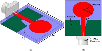
In this section ‘Single element antenna’, the complete analysis of the 2 × 2 MIMO antenna is studied and before this, the evolution of the single element antenna offering wider impedance bandwidth is developed. Figure 1 shows the isometric view as well as the front view of the antenna. Figure 1(a) which is the isometric view consists of an FR4 substrate with dimension L × W mm2 and thickness h = 1.60 mm. The radiating patch is printed on one plane and ground on the opposite plane of the substrate as observed in Fig. 1(b). The radiating patch which is connected to the microstrip feed line is attached to the 50 Ω SMA connector.
(a) Isometric view of proposed multiband antenna (b) Front view.

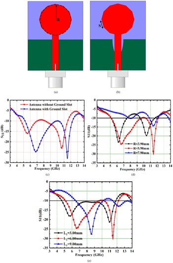
Figures 2(a) and 2(b) shows the evolution of the proposed antenna in two iterations and Fig. 2(c) compares the S 11 result of both the antennas. Figure 2(a) consists of a polygon patch with 12-sides and a rectangular ground. The equivalent circle of radius R forming the polygon is calculated by following equations [Reference Sharma, Awasthi and Singh27]


(a) Antenna #1: Without ground slot (b) Antenna #2: With ground slot (c) S 11 (Antenna #1 & Antenna #2). Parametric Study of (d) R (e) L1.

The effective radius of the patch antenna is given by

Also, the area of the polygon is given by

Antenna #1 shown in Fig. 2(a) provided the impedance bandwidth of 4.53–11.52 GHz. It can be observed that for the bandwidth between 7.02–8.32 GHz, the matching of impedance is very poor. However, to improve the deteriorated bandwidth, the modification of Antenna #1 is subjected by etching a semi-elliptical slot in the ground which not only improves the impedance bandwidth but also provides two resonant frequencies at 6.88 GHz (S 11 = −25.02 dB) and 11.52 GHz (S 11 = −28.31 dB).
The optimized impedance bandwidth which is obtained from Antenna #2 is dependent on two key parameters, one equivalent circle radius R and the slot length L 1 mm in the ground The two extreme values of R = 3.90 and 7.90 mm show that the antenna achieves wider impedance bandwidth but filters partial band from 7.52–9.51 GHz for R = 3.90 mm. The value of R corresponding to 7.90 mm observes a very high mismatch of impedance but, for R = 5.90 mm, the objective of the proposed work is achieved with a highly matched impedance bandwidth of 5.08–12.12 GHz. Similarly, another key parameter that contributes to the design of Antenna #2 is involved in the matching of impedance, thereby resulting in wider bandwidth. The semi-elliptical etched slot in the ground denoted by L 1 (major radius of the ellipse) with the value of 3.00 mm achieves an impedance bandwidth of 4.50–11.52 GHz and with the value of 9.00 mm the bandwidth is 6.51–10.10 GHz. In the former case, L 1 = 3.00 mm, in comparison to L 1 = 6.00 mm which is an optimized value with a bandwidth 5.08–12.12 GHz do achieve the objective but, the proposed work is extended to MIMO configuration with two band notched filters. Due to this, better matching of impedance is required which is fulfilled by L 1 = 6.00 mm.
MIMO configuration
The single-element antenna discussed in Figs 1 and 2 is an example of a single-input-single-output (SISO) communication system. This system when placed in a real-time communication system does suffer from drawbacks such as multiple-path fading and thus directly affects the working bandwidth of the antenna. Accordingly, Shannon–Hartley has given the advantage of using more than 1 radiating element which is called a multiple-input-multiple-output (MIMO) system and is defined as the maximum rate at which the signal containing the information is radiated over the wireless communication channel with the defined bandwidth of interest in the presence of noise.
However, in a real-time scenario (measurement in an anechoic chamber), the level of noise is 0 dB. The Channel Capacity (CC) for SISO is given by

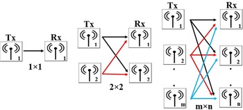
where CC 1×1 is Channel Capacity (b/s/Hz), B 1×1 is the operating bandwidth. In the absence of noise, CC 1×1 = B 1×1 which means completed bandwidth is utilized in the ideal case, but in a real scenario, the noise does exist, and also there will be multiple reflected signals received by the receiver. Figure 3 shows 1 × 1, 2 × 2, and m × n (m = n) MIMO configurations. It can be observed that, in the SISO system, the receiver will encounter multiple path fading effects, but in MIMO configuration, the receiver antennas will receive the signals all the time, and hence the modulated transmitted signal is preserved at the receiver. Also, equation (5) for channel capacity in absence of noise suggests that the bandwidth is multiple of several antenna elements present in a MIMO system. This concludes that MIMO configuration outclasses the SISO technology in comparison with mitigating the effects of signal interference noise ratio and thereby, preserving the operational bandwidth.
Different MIMO Configuration.

TCM analysis implementation on 2 × 2 MIMO configuration
The set of independent current vectors are analyzed by TCM theory which corresponds to different modes which naturally occur within the structure. By applying infinite number of modes, it can be easily calculated the closer resonances which are supported within the structure itself. As an antenna designer, the current patterns which naturally exist in the structure is valuable which helps in utilization of characteristic modes more attractive for antenna design, helping in obtaining physical insights into antenna radiation. Moreover, the quantative analysis of the characteristics angle (CA) and eigenvalues do dependent on the size or shape of the structure and, thus TCM analysis offers important role in designing the antenna for different wireless applications.
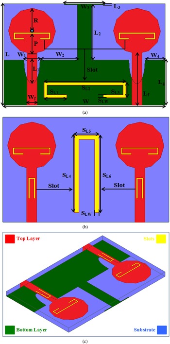
Figure 4 shows the configuration of the proposed 2 × 2 MIMO antenna configuration. The purpose behind the conversion of the single radiating antenna to a 2-port MIMO configuration is already discussed in section ‘MIMO configuration’ where the channel capacity of the MIMO antenna is increased without comprising the operational bandwidth. Figure 4(a) shows the front and ground view of the antenna. The front view of the antenna is printed on an FR-4 substrate with two identical 12-side polygon patches and a common shared ground which is printed on the opposite plane of the substrate.
Proposed 2-Port Design with Parameters; (a) Single Notch; (b) Dual Notch and (c) Isometric View.

As observed from Fig. 4(a), the radiating patch is etched by a rectangular slot which acts as the band-stop filter for interfering WLAN band (5.150–5 GHz). Also, the common-shared ground is etched by two semi-elliptical slots placed behind the microstrip feedline for better matching of the impedance. The isolation between the two radiating patches is taken care of by a T-shaped stub attached symmetrically to the ground. Figure 4(b) shows the etched U-type slot in the microstrip feed-line which mitigates downlink-uplink satellite (DUS) interference (7.25–8.30 GHz). The isometric view is represented in Fig. 4(c) with a different color legend showing various sections of the antenna. FR-4 substrate which is low cost and commercially available is used which also easily integrates with MMIC circuits. Two opposite planes of the substrate are used to print the isolated patch and shared common ground.
Recent time has seen the evolution of wireless technology in both narrow as well as wideband applications. These wireless applications have a wide range of implementations ranging from mobile phones to modern wireless communication say ships, aircraft, etc. The challenges encountered in designing these antennas have fuelled the advancement in the field of the antenna due to reasons such as the need for antennas with smaller physical size, lower weight, and cost, multi-wideband bandwidths, the capability of reconfigurable, etc. Therefore, the breakthrough in designing these antennas has emerged in the form of the TCMs [Reference Addepalli, Babu, Beno, Potti, Nageshwara, Sundari and Devana28–Reference Babu, Aldhaheri, Sai, Perli, Addepalli, Pasumarthi, Kumar and Devana30] which gives freedom to analyze the physics behind the key attributes including bandwidth polarization and distribution of surface current density (SCD) on a patch of antenna and ground. The theory behind TCM is older than 50 years which was proposed by Garbacz in 1965. This theory correlates the surface current distribution on PEC bodies (perfect electric conductor) which is decomposed to several modal currents and each of these radiates the respective characteristic modal pattern. The key parameters which are evaluated by characteristic mode analysis include modal significance, CA, and eigen current. The impedance matrix associated with Eigen current is given by


where Z is the total complex impedance, R and X are the real and imaginary parts of the impedance.
The weighted Eigen equation is given by

where Jn is the eigenvector, en is the eigenvalue and the W is chosen matrix. The generalized
form of eigenvalue equation can be written as

The above Equation can also be derived by using Poynting's theorem [Reference Chen and Wang1] achieving the same result. The characteristic field is defined as the far-field due to modal currents and is given by


By interchanging m and n

It is known that


In far-field, the characteristics field is given by

were $\hat{k}$ is the unit vector.
The characteristic current, δ mn in terms of electric field € and magnetic field (H) is given as


This shows the characteristic field from the orthogonal set (in far-field). It can also be concluded that both, polarization and magnitudes of characteristics fields are orthogonal to one another.
The Eigen-value λ n, between electric and magnetic field concerning m and n coefficients, is given by

Also,

For m = n in equation (20), a few important conclusions are derived which are given below
(1) The magnitudes of the eigenvalues are directly proportional to the total stored energy field
(2) For λn = 0, it indicates that the energy stored (electric and magnetic) are equal and hence, the resonance condition is achieved
(3) For λn > 0, the stored magnetic field is more dominant than the stored electric field and hence, is known as inductive modes
(4) For λn < 0, the stored electric field is more dominant than the stored magnetic field and hence, these modes are known as capacitive modes
The expansion of the induced currents and far-field due to the external source for characteristics modes are completely set of orthogonal modes. The characteristic current for a PEC body (patch/ground) is represented as

The far-field electric and magnetic field produced by the external source due to induced current is given by

Substituting equation (21) in $\lceil{L( J ) } \rceil _{\tan } = E_{\tan }^r ( r ) , \;\;r\epsilon S$

Inner-product of equation (23) gives

were Jm is the characteristic current and Z is the impedance matrix. For m = n, and applying the property of orthogonality for the characteristic current in the above equation, the following equation (25) is evolved which is given by


here $\left\langle {E_{\tan }^i \;( r ) , \;\;J_n} \right\rangle$ is the modal excited coefficient and hence, modal significance (MS) is given by

The key point to be noted irrespective of modal significance is that it provides the ease of measuring the bandwidth and thus half-power bandwidth $\left({\left({1/\sqrt 2 } \right) = 0.707} \right)$ is given by

were fH, fL and f ees are the resonance and at f res, MS is given by


This concludes that for MS > 1/$\sqrt 2$ corresponds to significant modes and MS < 1/$\sqrt 2$
 is the non-significant mode.
Also, when different modes are applied to PEC, there will be constant phase lag between real current Jn and also the equal-phase for $E_n^{\tan } ( S )$ . The constant phase lag (αn) between the two is given by 1

This indicates that the phase lag is directly calculated from the eigen value and for α n = 180° indicates resonance otherwise the modes are said to be internal or cavity resonance for α n = 90° or 270°. Thus for α n = 180° the modes are resonance modes, 90° < α n < 180°, the modes are inductive and for 180° < α n < 270°, the modes are capacitive.
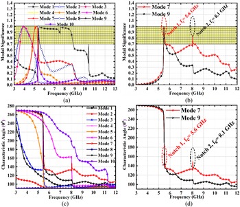
The 2-port MIMO antenna configuration is developed by using the TCM shown in Fig. 5. In the proposed 2-port MIMO configuration, ten modes are subjected which can be observed in Figs 5(a) and 5(c) including two interfering filters (WLAN and DUS). The $MS \gt \left({1/\sqrt 2 } \right)$ for mode 1, mode 3, mode 5, mode 6, and mode10 which are the significant modes. Therefore, these five modes are responsible for the wider impedance bandwidth. Also, it can be observed that the resonance values of a frequency corresponding to 3.54 GHz (mode 1), 3.68 GHz (mode 3), 5.20 GHz (mode 5), 6.32 GHz (mode 6), and 8.20 GHz (mode 10). Figure 5(b) shows the two modes (mode 7 and mode 9) exclusively play a vital role in notching the two interfering bands. The CA is represented in Figs 5(c) and 5(d) for the dual notched band 2-port MIMO antenna. It can be noted that αn = 180° at 3.54, 3.68, 5.20, 6.32 and 8.20 GHz corresponds to resonance modes. In mode 7 and mode 9, the CA values correspond to 168° (5.52 GHz) & 150° (8.10 GHz) are the inductive modes.
Characteristics mode analysis (a) MS for dual notched band MIMO antenna (b) MS for two notched bands (c) CA for dual notched band MIMO antenna (d) CA for two notched bands.

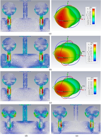
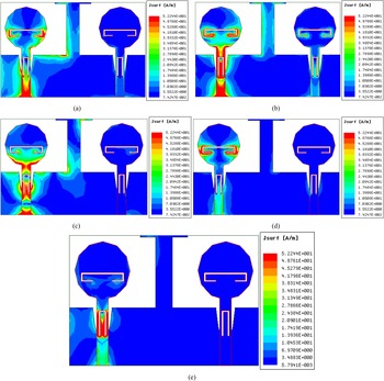
Figures 6(a)–6(e) shows the distribution of surface current which is initiated for mode 1 (3.54 GHz), mode 5 (5.20 GHz), mode 10 (8.20 GHz), mode 9 (5.60 GHz), and mode 7 (8.10 GHz). The significant modes shown in Figs 6(a)–6(c) offer an even distribution of surface current and hence the MIMO antenna radiates the signal efficiently with good Omni-directional and di-pole patterns in both the planes. In the case of Figs 6(d) and 6(e), the current vectors cancel with each other and hence there is no radiation. Table 1 gives the parameter values of the MIMO configuration shown in Fig. 4.
Proposed Design: (a), (b), and (c) are Surface Current Distribution with 3D-Radiation Patterns; (d) & (e) are only Surface Current Distribution at Notched Bands. (a) 3.54 GHz (mode 1) (b) 5.20 GHz (mode 5) (c) 8.20 GHz (mode 10) (d) 5.60 GHz (mode 9-Notched) (e) 8.10 GHz (mode 7-Notched).

Proposed design parameters with values

Evolution of the 2-port MIMO antenna, input impedance, and time domain analysis
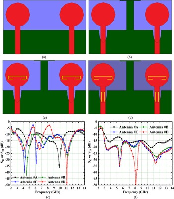
The evolution of the proposed 2 × 2 MIMO antenna is shown in Fig. 7 with a comparison of reflection as well as transmission coefficient results. Figure 7(a) which is designed as Antenna #A is formed by placing two polygon patches adjacent to each other and commonly shared
Evolution of the proposed antenna (a) Antenna #A (b) Antenna #B (c) Antenna #c (d) Antenna #4 (e) S 11/S 22 result (f) S 12/S 21.

rectangular ground. This offers the operating bandwidth of 4.02–10.92 GHz as shown in Fig. 7(e). Also, from Fig. 7(f), it can be seen that the isolation between the two ports is very poor. To improve the impedance bandwidth and to achieve higher isolation, Antenna #B is reported which has two modifications, one semi-elliptical slot in the ground to improve the bandwidth and the other, the T-shaped stub attached to the ground plane. The S 11/S 22 −10 dB bandwidth corresponds to
3.03–12.38 GHz with two resonances at 4.38 GHz (S 11 = −42.31 dB) and 11.52 GHz (S 11 = −27.61 dB). The isolation of Antenna #B is also improved with S 12/S 21 being more than 15 dB. The impedance bandwidth generated by Antenna #B also occupies other wireless communication applications such as WLAN and DUS. These two bands impact as interference and have to be mitigated. Band stop filters which are the solution to the above two said interference are added to Antenna #B in the form of an etched C-type slot on the radiating patch (Antenna #C) and a U-shaped slot in the microstrip feed-line (Antenna #D). Antenna #C shown in Fig. 7(c) occupies the operational bandwidth of 3.00–11.18 GHz with filtered WLAN interference (5.02–5.89 GHz). Similarly, the final version of the required MIMO configuration is achieved by Antenna #D which filters WLAN and DUS interfering bands. On the other hand, the MIMO configuration
Also shows the isolation of more than 15 dB with maximum isolation of −35, −50 and −34.8 dB is noted at 5.32, 8.10 and 11.22 GHz respectively.
The effect of the parameters shown in Table 1 is the optimized parameters. However, when their values are changed, they do affect the operating bandwidth which indicates the change in the value of overall impedance. In this proposed study, key parameters affecting the notched bandwidth are investigated. The quarter-wavelength for both the notched bands are calculated from equations (32) and (33) given below.

where L IB is the length of the interfering band in mm, f r is the center frequency of the corresponding notched band, k is the speed of light which is 3 × 10⁸ m/s, and ɛ reff. is calculated by

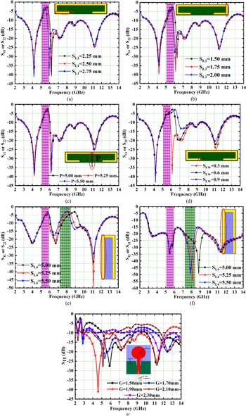
These equations suggest that the total length of the stub is dependent on the center notched frequency, effective permittivity, the height of the substrate, and the width of the microstrip (W f). However, the electrical parameter such as effective permittivity, the height of the substrate, and with of the microstrip are static values. So. By changing the L IB, the center notched frequency will also change. For the WLAN interfering band, the total overall length of the stub id L IB = S L2 + 2(S L3 + S L1). Thereby, changing the value of S L3 and S L1 will also change the shifting of the notched frequency corresponding to WLAN interference. Figures 8(a) and 8(b) shows the change of S L1 from 2.25 to 2.75 mm which records the shifting of the band from the lower to higher frequency side. However, for S L1 = 2.50 mm the intended WLAN interference is mitigated. Also, the parameter associated with WLAN notched filter slot, S L3, is varied between 1.50 to 2.00 mm. For S L3 = 1.75 mm, which is an optimized value that ensures the removal of the WLAN interfering band. Similarly, the position of the WLAN slot with distance P mm is changed from 5.00 to 5.50 mm observing a very negligible change in the position of the WLAN notched bandwidth. However, for P = 5.25 mm, the optimized result is obtained for the WLAN interfering band. The thickness of the rectangular slot S LW, however, has a large impact on the WLAN notched bandwidth as shown in Fig. 8(d). So for S LW = 0.60 and 0.90 mm, the notched bandwidth widens and more frequencies are included which is extended beyond WLAN. For S LW = 0.30 mm, the exact WLAN notched band is achieved. Figures 8(e) and 8(f) shows the effect of change in length S L4 on reflection as well as on transmission coefficient. The total physical length corresponding to DUS interfering band is L IF = S L5 + 2S L4. For the value of S L4 = 5.25 mm, the intended DUS notched band is achieved while for the other two values of S L4 = 5.00 and 5.50 mm, the out of required notched band is filtered, and also, during the optimization process, the WLAN band is not affected which concludes that the two interfering band are independent to each other. Figure 8(g) shows the parametric variation of the gap G between the radiating patch and the ground. For G = 1.50 mm, the antenna offers bandwidth of 2.74–2.92 GHz, 5.11–8.71 GHz and 10.08–12.00 GHz. The gap G = 1.70 mm offers an impedance bandwidth of 2.76–3.09 GHz, 4.26–8.64 GHz and 11.12–12.0 GHz. However, for the above-said values, the required bandwidth is not obtained. On the other hand, for higher values of G = 2.10 & 2.30 mm, the partial bandwidth is achieved. For G = 1.90 mm, which is an optimized value provides operational bandwidth useful for both UWB and X-band applications.
Proposed 2-Element Design Parametric Study; (a) S L1; (b) S L3; (c) P and (d) S LW; (e) S L4 for S 11 and (f) S L4 for S 21 (g) G.

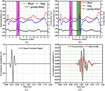
To have more insight into the working of the proposed 2-port MIMO antenna, SCD distribution on patch and ground is studied which is shown in Fig. 9. Figures 9(a) and 9(c) shows the SCDD for the three selected frequencies 4.00, 6.60 and 11.20 GHz. The simulation is carried out by giving input at Port 1 and the other Port 2 is terminated in characteristics impedance of 50 Ω. In all three cases, it can be seen that the SCDD is concentrated evenly on the patch other than the feed-line. This shows that all the input signals are radiated efficiently. However, the feed-line is not the part of the radiation which is used only as a transmission line between the input port and the transmitting antenna. Interestingly, the isolation element which is in the form of a T-shaped stub and attached to the ground plays important role in providing higher isolation. This is due to the concentration of current flow from the ground behind the antenna where input is given towards the T-shaped stub (shown by arrow). This phenomenon is observed in all three frequencies centered at 4.00, 6.60 and 11.20 GHz respectively. This justifies the addition of a T-shaped stub in achieving higher isolation and also there is almost nil interference in Antenna #2. However, for 6.60 GHz, there is slight interference in Antenna #2 from Antenna #1 which is due to the isolation value of −15 dB. Figures 9(d) and 9(e) shows the SCDD for the two center-notched frequencies 5.60 and 8.10 GHz. The C-type rectangular stub is used as a filter for the WLAN interfering band, all the SCD is accumulated around the slot which indicates the mismatch of impedance. Similar observations are noted for the DUS center notched frequency 8.10 GHz with all the SCD being on the U-type slot etched in the microstrip line. It is worth noting that the T-shaped stub which is used to achieve isolation between the two radiating elements has no role to play during the two filtering bands (WLAN and DUS). Figure 10 shows the plot of impedance and time response of the proposed 2 × 2 MIMO antenna with group delay & impulse response. Figures 10(a) and 10(b) shows the real and imaginary impedance for single and dual-notched bands.
Proposed Design Surface Current Distribution; (a) 4.0 GHz; (b) 6.6 GHz; (c) 11.2 GHz; (d) 5.6 GHz (Notched Band) and (e) 8.1 GHz (Notched Band).

Proposed Design Time Response Analysis; (a) Input Impedance & Group Delay (Single Notch) and (b) Input Impedance & Group Delay (Dual Notch) (c) Input Impulse (d) Received signal in two orientations.

Figure 10(a) shows the real impedance value almost follows the 50 Ω and imaginary impedance to 0 Ω. However, at the WLAN notched band, there is a high mismatch of the impedance due to the introduction of a band-stop filter in the form of an etched C-shaped slot on the radiating patch. At, this band, the maximum real value of impedance corresponds to 300 Ω at 5.68 GHz and two values of imaginary impedance at 148/−148 at 5.56/5.82 GHz. Similarly, Fig. 10(b) shows the real and imaginary impedance plot for the additional DUS band which was achieved by etching an inverted U-type slot on the microstrip feed-line. For the real value of impedance at notched bands, the maximum values are 225 and 300 Ω at 5.44 and 8.32 GHz. Also, there is a large deviation observed for imaginary impedance at these two notched bands. Figure 10 also examines the time response of the antenna as it becomes necessary due to the wideband bandwidth. Group delay is generally used to characterize the two antennas, one transmitter, and the other receiver. Group delay is used to measure the delay of the signal and the distortion in phase. Thus, the group delay is defined as the derivation of the phase-response and is given by

The Group Delay, in the ideal case, is expected to be a constant value with no variations but, the change of ±1 ns is acceptable which preserves the shape of the received pulse without distortion. Figures 10(a) and 10(b) shows the plot of Group Delay for single and dual notched band MIMO antenna. In both, cases, the operating bandwidth of interest to preserve the values of Group Delay is between ±1 ns except in the notched bands (WLAN and DUS). Figure 10(c) represents the input impulse which is from the family of Gaussian is fed to the transmitter and observed the shape of the pulse at the receiver with ensuring far-field region. Figure 10(d) shows the received pulse in two orientations, one face-to-face and side-to-side. The receiver when placed in face-to-face orientation receives a more faithful signal than in side-to-side orientations. It can be also observed that the ringing effects are noted in received pulses which might be due to the reasons for undesired energy stored or multiple reflections. This ringing affected is more prominent in the SISO system and much improved in MIMO technology. The correlation coefficient between the transmitter-receiver signifies the similarity between the two is given by

here S Tx (t) is the transmitted signal and S Rx (t) is the received signal with τ being the delay of the received signal. The transmitted and received pulses are matched when the fidelity factor is 1. The correlation coefficient corresponds to 0.88 and 0.82 for face-to-face and side-to-side orientation.
Discussion of results and diversity performance
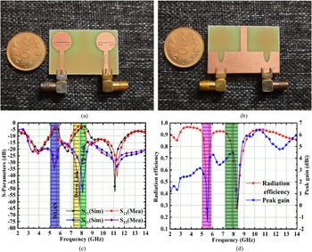
To verify the analysis of the 2 × 2 MIMO antenna configuration which was developed by using Characteristics Mode Analysis needs to be compared with the measured results. This is achieved by fabricating the prototype and comparing the measured results with the simulated. The fabricated prototype shown in Figs 11(a) and 11(b) with two isolated radiators placed adjacent to each other and ground with isolation stub on an opposite plane is printed on FR4 substrate. A matched SMA connector that works up to 18 GHz is connected to a match 50 Ω microstrip line. Also, Fig. 11(c) shows the comparison of simulated and measured results between the reflection coefficient (S 11) and transmission coefficient (S 21). In both cases, there is close agreement between the simulated and measured results, thus validating the proposed 2 × 2 MIMO design. Figure 11(d) also shows the result of Normalized Radiation Efficiency and Peak Gain (dBi) of the MIMO antenna. As per the observations, in the working bandwidth, the MIMO antenna maintains the radiation efficiency of more than 0.90 or 90%, but at the notched bands, the radiation efficiency falls to 0.25 at 5.43 GHz and 0.28 at 8.39 GHz respectively. Figure 11(d) also shows the measured peak gain (dBi) of the proposed antenna with the rise in peak gain from a lower to a higher frequency. The variation of the gain is between 2.20–6.50 dBi with a peak gain fall of −1.52 dBi at 5.52 GHz and −0.92 dBi at 8.38 GHz respectively.
Fabricated prototype (a)-(b) Front and Ground View (c) S 11/S 22 & S 12/S 21 result (d) Normalized Radiation Efficiency & Peak Gain (dB).

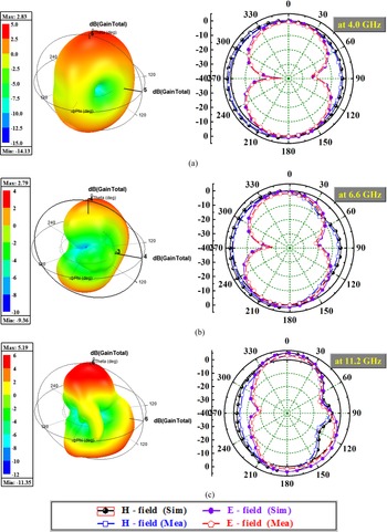
The fall in radiation efficiency and peak gain I notched bands is due to the reason that the antenna is not radiating the signals but blocks them due to the mismatch of impedance. Another important result related to the far-field of the MIMO antenna configuration is shown in Fig. 12 which shows 3-D as well as 2-D radiation patterns. These radiation patterns are plotted at three different frequency points selected in the operational bandwidth of the antenna. The radiation pattern at 4.00, 6.20 and 11.20 GHz shows the dipole and Omnidirectional pattern in both the principal planes. However, at a high frequency, 11.20 GHz, there is acceptable deterioration in both the radiation planes which may be due to an increase in the area of radiation. Thus the proposed antenna can be used for a wide range of frequency bandwidth in either E or H-planes. Figure 11(c) shows the simulated and measured S-parameters plays a vital role in defining the Diversity Performance of any MIMO antenna configuration. The better the matched impedance, the better the S-parameters. However, the T-shaped stub attached to the ground has been a value-added in design as it maintains the isolation of more than 15 dB in both simulation and measured environments.
Proposed Design 3D-Polar plot and E&H Fields Patterns; (a) 4.2 GHz (b) 6.2 GHz (c) 11.2 GHz.

The correlation between the antenna elements and the isolation is signified by ECC. In ideal conditions, ECC is zero but in an actual free space condition environment, ECC will have non-zero values.
The ECC can be calculated between any two ports of the proposed 2 × 2 MIMO antenna by using the radiation field pattern and S-parameter between the two ports. The ECC Equation using field-pattern is given by

Equation (36) can be analyzed as the excitation of the say ith port whose radiation field pattern is calculated while all the other ports are terminated by matched 50 Ω impedance. Let there be N number of MIMO antenna system (N = 2 in the proposed antenna system), the ECC between any of the two antennas (Simulated and Measured: ECC12(2×2)) is calculated as

where Ci,j(N) is given by

Comparing equations (37) and (38) is given by

Equation (40) calculates ECC for two port MIMO antennas (Ant. A and Ant. B) and is given by

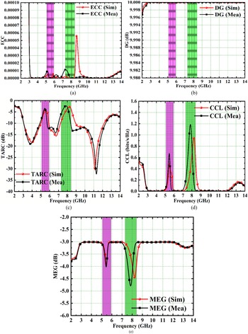
The expected or the ideal values for ECC < 0.50 for any MIMO antenna configuration. Figure 13(a) shows the simulated and measured ECC values. It can be seen that the simulated ECC for any two antennas combination in both simulated and measured results are well below the permissible values indicating good isolation achieved due to the decoupling elements and the values are below 0.00001 but, for notched bands, these values are high due to the lower values of S-parameters.
Diversity performance: Simulated and Measured (a) ECC (b) DG (c) TARC (d) CCL (e) MEG.

The Diversity Gain of the proposed 2 × 2 MIMO antenna is calculated by equation (41) given below

Equation (41) shows DG(2×2) is a MIMO diversity parameter that is dependent on ECC(2×2). It can be also understood that the power reduction when the diversity scheme is introduced in a 2 × 2 MIMO antenna configuration. The lower the values of ECC, the better the Diversity Gain. Ideally, the DG > 9.95 dB and in the designed antenna, simulated and measured DG values are greater than 9.999 dB in the entire operating bandwidth.
It can be expected that when the MIMO configuration is formed, the radiating elements which are placed closely will affect the performance of the MIMO antenna configuration. Hence, just by using S-parameter alone, the performance of the MIMO antenna cannot be judged and hence, there arises a need to define a new metric called Total Active Reflection Coefficient (TARC) which is calculated by

Further, TARC can be defined as “the square root of the ratio of total incident power and its apparent return loss” of the MIMO antenna configuration. Ideally, the TARC is <0 dB for the MIMO communication channel. In Fig. 13(c), the simulated and measured TARC values are less than −10 dB.
Channel capacity can be defined “reliable transmission of signal or information with a maximum rate of over the channel used and with no distortion” and the information loss associated with the MIMO communication channel is termed Channel Capacity Loss (CCL) which is calculated by

where

where


The CCL in the MIMO communication channel should not be more than 0.40 bits/s/Hz. In the proposed work, as per the observations in Fig. 13(d), these values are less than 0.02 b/s/Hz for all the possible two port combinations. Also, in all the two notched bands, the CCL corresponds to 0.63 and 7.92 b/s/Hz which is due to the bandstop filters.
The antenna receiving averaged signal is computed by the diversity parameter known as Mean Effective Gain (MEG) and is defined as the ratio of the power received by the receiving antenna to the total power which is incident on it. The MEGs are calculated between any two antennas given by generalized formula given for mth and nth antenna


The ratio calculates the MEG which is given by

For the proposed antenna MEGs are calculated for Antenna #1-Antenna #2 were simulated and measured values are plotted in Fig. 13(e). As per the observations, the ratio of MEG values is approximately −3.0 dB for both simulated and measured values in the operating bandwidth of interest.
Comparison of proposed work with present-state-of-the-art
Table 2 shows the comparison of the proposed MIMO antenna with earlier published work. The compact MIMO antenna is fabricated on a commercially available FR4 substrate which is very easy to integrate with other PCB circuits such as filters, amplifiers, etc. The proposed antenna also offers good isolation and outclasses other reported work in terms of diversity performance parameters. The proposed MIMO antenna is suitable for multiple wireless applications in UWB and X-Band.
Comparison of proposed work with other published articles

P, Proposed; ■, Connected Ground; □, Isolated Ground; NC, Not Calculated
Conclusions
A very low profile 2-port MIMO antenna assisted by TCM is proposed in this research. The radiating element consists of two 12-sided polygon patch which is placed adjacent to each other with a common shared rectangular ground which is etched by two elliptical slots and an embedded t-shaped stub that provides isolation between the two ports. Also, the proposed MIMO antenna is capable of mitigating two interfering bands: WLAN and DUS which are achieved by etching slots. It is also demonstrated in the proposed work that the polygon patch excited seven CMs (two significant modes for operating bandwidth and two for notched bands). The measured results obtained from the fabricated prototype offer a working bandwidth of 3.11–11.68 GHz. Also, the mutual coupling is more than 15.0 dB in the UB- band spectrum. The diversity parameters include ECC < 0.00001, DG ≈ 10.0 dB, TARC < −15.0 dB and CCL < 0.001 b/s/Hz. The proposed MIMO antenna offers good 2-D/3-D radiation patterns for a wide range of frequencies with a radiation efficiency of more than 90% & maximum peak gain of 6.50 dBi suggesting the proposed work is a good candidate for multiband applications.
Data
Our manuscript has no associated data.
Conflict of interest
We declare that there is no conflict of interest among the authors.
 Dr. Manish Sharma received B.E. degree in electronics and communication engineering from Mangalore University, Karnataka, India in 2000 and M.Tech. degree from Visvesvaraya Technological University, Karnataka, India in 2007. He completed his Ph.D. degree from the Department of Electronics Engineering, Banasthali University, Rajasthan, India in 2017. He is currently working as professor-research in Chitkara University Research and Innovation Network (CURIN), Chitkara University, Punjab, India. His research interest includes computational electromagnetics, reconfigurable antennas, novel electromagnetic materials, dielectric resonator antennas, wideband/superwideband antennas, wideband/dual band/triple band microstrip antennas for wireless communication, smart and MIMO antennas systems, radio-frequency identification (RFID) antennas, antennas for healthcare, RF MEMS planar antenna on Si substrate, wireless networks, body area networks, meta surface based biosensors, Designing of Microstrip antennas using Machine Learning and Artificial network. He has published more than 100 + research articles in SCI/SCOPUS Indexed Journals and also 8 patents are granted in his name. He has guided two Ph.D. students and currently there are 8 Ph.D. ongoing scholars.
 Dr. Tathababu Addepalli was born in 1986, A.P., INDIA. He received his B. Tech. degree from JNTUH, Hyderabad in 2007, M. Tech. degree from JNTUK, Kakinada in 2010 and Ph.D., degree from JNTUA, Anantapur in 2022. Currently, he is working as associate professor in the department of ECE at Aditya Engineering College (A), Surampalem, Kakinada, A.P., INDIA. He has published ten (11) SCIE research papers in various reputed international journals like Elsevier (International Journal of Electronics and Communications (AEU)), Wiley (International Journal of Communication Systems (IJCS)), MDPI (Electronics), Springer (Wireless Personal Communications (WPC)), Wiley (Transaction on Emerging Telecommunication Technologies (ETT)), Elsevier (Alexandria Engineering Journal (AEJ)) and Taylor & Francis (Journal of Electromagnetic Waves and Applications), presented 5 Conferences (4 IEEE, 1 Springer), published two book chapter on THz antennas and planar antennas. He attended more than 40 workshops in various reputed institutions. His areas of interest are microstrip patch antennas, MIMO antennas, 5G antennas, flexible antennas, characteristic mode analysis (CMA), THz antennas and metamaterial antennas.
 Dr. Rajasekhar Manda currently working as associate professor in ECE Department, PACE Institute of Technology & Sciences (A), Ongole. He received early Education from Kandukur, Prakasam District. B.Tech. in electronics and communication engineering from college Prakasam Engineering College, Kandukur in 2009, obtained M.Tech. in 2011 from Adam's Engineering College, Paloncha with systems and signal processing as specialization. He worked in Sri Aditya Engineering College from 2011 to 2013 as assistant professor. After that he secured the AURCET 4th Rank and joined research as full time scholar in AU College of Engineering (A), Andhra University, and Visakhapatnam in March 2014. He qualified the UGC-NET three times consecutively in June-2012, December-2012 and June-2013 (junior research fellow). During his research work, he received stipend from UGC-New Delhi for two years as junior research fellow (JRF) and 3 years as senior research fellow (SRF). In addition to it, he served in organizing committee for several workshops & conferences. He has published papers in Journal, National and International Conferences and received doctoral degree in area of radar signal processing under the guidance of Prof. P Rajesh Kumar, Chairman BoS, AUCE(A), Visakhapatnam in 2011. His field of interest is antennas and radar signal processing. He has been attending over 75 + National workshops/Webinars since 2011. He is member of IEEE, associate member of IETE & IE, life member of Indian Science Congress Association (ISCA), India Science for Technical Education (ISTE), IAENG, IFERP, ISST and. He taught several subjects in electronics and communication engineering since 2011. He loves teaching, has interest in research and knowledge sharing and strongly believes in hard work.
 Dr. Thota Vidyavathi received her B.Tech. degree from JNTU Hyderabad in the department of electronics and communication engineering during the year 2006 and the Master of Technology in radar and microwave engineering from Andhra University College of Engineering (A) in the year 2008. She was awarded Ph.D. degree in the year 2015 from the dept. of ECE, Andhra University. She has worked in Gayatri Vidya Parishad College of Engineering College(A) during the period July 2015 to August 2022. Currently, she is working as associate professor in the department of ECE, Anil Neerukonda Institute of Technology and Sciences (A), Visakhapatnam, Andhra Pradesh, India. Her research interests include array antennas, electromagnetic theory and wave propagation, radar engineering, microwave engineering, EMI/EMC, computational electromagnetics and soft computing. She has guided more than 20 UG and PG projects. She is a member of IEEE antennas and Propagation Society; she is life member of Society of EMC Engineers- SEMCE (India) also a member of International Association of Engineers (IAENG) and International Association of Academic plus corporate (IAAC). She is a fellow member of IETE; she is recipient of YOUNG SCIENTIST AWARD-March 2020, YOUNG WOMEN RESEARCHER AWARD-February 2022; presently, she is working in the area of array antennas design by using HFSS software simulation. She has three patents and published in various reputed national and international journals. She is a paper reviewer for various Scopus and SCI indexed journals. She has organized and coordinated various international conferences, technical workshops, faculty developments programmes and given guest lectures in the department.
 Dr. Prabhakara Rao Kapula is presently working as a professor at the Department of Electronics and Communication Engineering, B V Raju Institute of Technology, Narsapur, Telangana. He has teaching experience of 22 years. He received his Ph.D. from Andhra University in 2017. He received his B.E. in electronics and communication engineering from Andhra University in 1996 and M.Tech. in instrumentation and control systems from JNTU College of Engineering, Hyderabad in 1999. His areas of interest include wireless communications, MIMO antennas and assistive devices for health care. He has published more than 50 + research articles in SCI/SCOPUS indexed journals and also granted one patent.